

Page 1
QUICK START GUIDE FOR DEMONSTRATION CIRCUIT 1242A
600MA SYNCHRONOUS BOOST DC/DC CONVERTER AND 100MA LDO REGULATOR
LTC3537
DESCRIPTION
Demonstration circuit 1242A includes a high efficiency synchronous boost converter, a low
dropout linear regulator and a low battery detector. With a light load, the boost converter can
startup with an input voltage as low as 680mV
and once started, the input can go as low as
500mV while maintaining a regulated output
voltage. With a 50mA load, the linear regulator
features a dropout voltage of less than 100mV.
Separate input terminals are provided for the
boost and linear regulator, and a jumper that
allows the linear regulator to be powered from
any one of three different sources.
Terminals and jumpers for shutting down or sequencing each regulators output separately and
individual Power-Good outputs are included.
Jumpers are also provided for selecting a total
of six output voltages, three low battery voltages and a jumper to select BURST or PWM
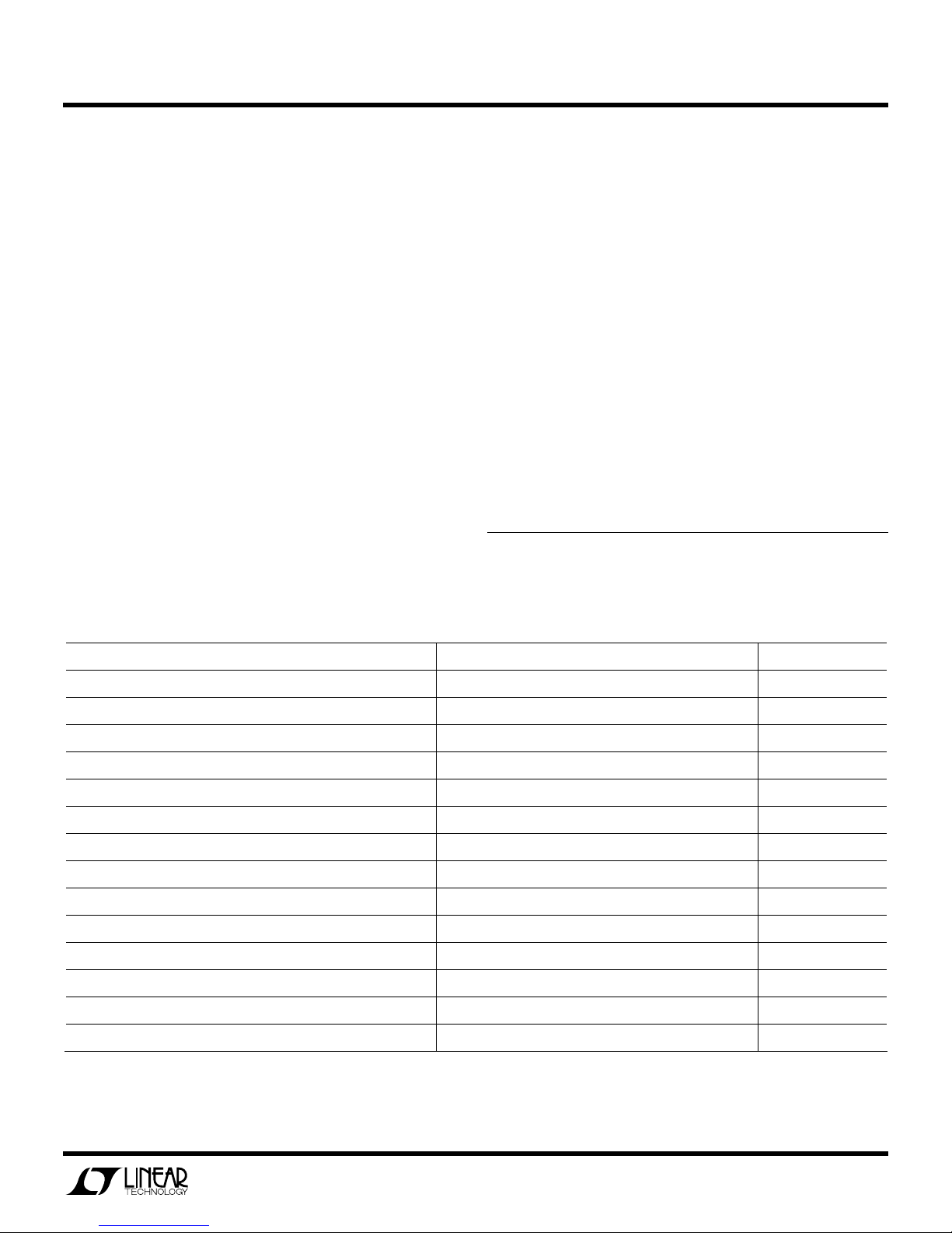
Table 1. Typical Specifications (25°C)
operation. The 3X3 mm QFN thermally enhanced package with a 2.2MHz switching frequency combined with the LDO regulator provide a very tiny multi output solution. The
LTC3537 boost converter also features output
disconnect and the input voltage can be greater
or less than the output voltage.
This demonstration circuit allows the user to
quickly evaluate the LTC3537 performance.
Jumpers make selecting different output voltages and low battery thresholds simple while
terminals on the board allow easy hookup to
input supplies and output loads.
Design files for this circuit board are available.
Call the LTC factory.
LTC and Burst Mode are trademarks of Linear Technology Corporation
Conditions Limits
Input Voltage Range VIN 0.68V to 5.5V
Boost 1.8V V
Boost 3.3V V
Boost 5V V
Output Ripple Voltage (burst mode) VIN = 1.5V, V
Output Ripple Voltage (fixed frequency) VIN = 1.5V, V
Boost Efficiency VIN = 1.8V, V
LDO Regulator 1.5V V
LDO Regulator 3.0V V
LDO Regulator 3.3V V
LDO Regulator Drop Out Voltage V
Low Battery Threshold Voltage (dropping) 0.8V 800mV ± 5%
Low Battery Threshold Voltage (dropping) 1.7V 1.7V ± 5%
Low Battery Threshold Voltage (dropping) 3.0V 3V ± 5%
VIN = 1V, I
OUT
VIN = 1.5V, I
OUT
VIN = 1.5V, I
OUT
VIN = 5V, I
OUT
VIN = 5V, I
OUT
VIN = 5V, I
OUT
OUT
OUT
OUT
OUT
OUT
OUT
OUT
= 3.3V, I
= 100mA 1.8V ± 3.5%
= 200mA 3.3V ± 3.5%
= 200mA 5.0V ± 3.5%
= 3.3V I
OUT
= 3.3V I
OUT
= 3.3V I
OUT
= 50mA 1.5V ± 2.5%
= 50mA 3.0V ± 2.5%
= 50mA 3.3V ± 2.5%
= 50mA,
OUT
= 15mA 30mV p-p
OUT
= 200mA 10mV p-p
OUT
= 100mA 88%
OUT
V
drops 10%
OUT
100mV
1
Page 2
QUICK START GUIDE FOR DEMONSTRATION CIRCUIT 1242A
Select VOUT
Select VOUT
600MA SYNCHRONOUS BOOST DC/DC CONVERTER AND 100MA LDO REGULATOR
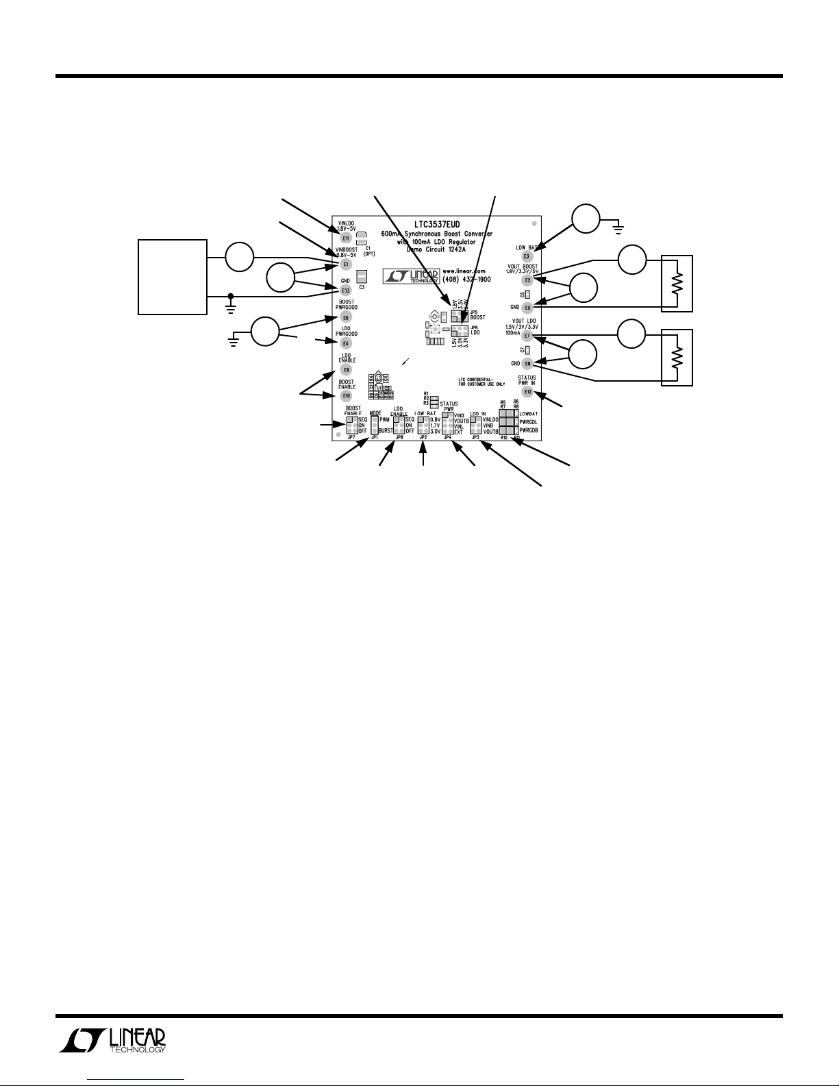
Figure 1. Demonstration Circuit Test Setup
LDO Input
BOOST Converter Input
A
Input
Power
Supply
+
-
PWRGOOD
STATUS Outputs
LDO & BOOST
ON/OFF Inputs
V
V
or
Select BOOST
ON/OFF/SEQ
Select
PWM
or BURST
Mode
QUICK START PROCEDURE
BOOST Regulator
Select
LDO
ON/OFF
or SEQ
Select
LOW
BAT
threshold
LDO Regulator
Low BAT
STATUS Outputs
V
Resistive
Loads
BOOST
A
V
A
V
LDO
Select
STATUS
power
source
EXT. STATUS
power source input,
select with JP4
Note:
resistors can
be replaced
Select LDO
input supply
with LEDs
The LTC3537 circuit can be evaluated using
the setup shown in Figure 1. Most of the features can be verified simply by placing jumpers in various locations. It is recommended
that the LTC3537 data sheet be nearby for a
more complete explanation of the various features and specifications.
Using jumpers JP5 and JP6, select the desired output voltages (with no jumpers installed, the output voltages are set for the
highest voltage). Enable each regulator by
placing jumpers JP7 and JP8 in the ON position and place the “LDO IN” jumper (JP3) to
the “VINB” (center) position which parallels
the LDO and BOOST supply inputs. Set the
“STATUS PWR” jumper (JP4) to the “VOUTB
position, which connects the open-drain
power good outputs and the low battery output pull-up resistors to the output of the boost
regulator. JP4 also allows an external voltage
applied to the STATUS PWR IN terminal to be
used for the pull-up resistors.
Connect voltmeters and ammeters as shown
in the Figure 1 test setup. Connect a power
supply to the VINBOOST and GND terminals
and a suitable load resistor between VOUT
BOOST and GND. Avoid excessive wire
lengths between the input power supply and
the demonstration board. Wire lengths greater
than 18 inches may require additional capacitance near the input terminals.
With a light load (1k resistor) at the output,
begin increasing the input power supply voltage. At approximately 700mV, the output will
rise to the selected regulated voltage. When
the output voltage exceeds the input voltage
by at least 240mV, the converter powers itself
from the output instead of the input. This feature allows the input voltage to drop as low as
500mV (at light loads) and still maintain a
2
Page 3

QUICK START GUIDE FOR DEMONSTRATION CIRCUIT 1242A
600MA SYNCHRONOUS BOOST DC/DC CONVERTER AND 100MA LDO REGULATOR
regulated output voltage. A data sheet curve
shows the minimum resistive load vs. Vin that
will allow the boost converter to start.
Increase the input voltage to approximately
1.5V or more and increase the load current.
The maximum load current depends on the
input and output voltage settings. A data sheet
curve shows the maximum output current for
different input and output voltages.
The PWRGOOD output terminals are high
when the output voltages are in regulation and
pull low if the output voltage drops by approximately 10%, for any reason.
The LOW BAT output terminal is high when
the voltage present on the VINBOOST terminal is greater than the voltage threshold selected by jumper JP2.
The input voltage can exceed the output voltage and still maintain regulation, although the
load current is less and efficiency is lower.
When Vin is near VOUT and in the range of
approximately 300mV to 100mV below Vout,
the converter is approaching the switch minimum ON time resulting in an increased output
voltage ripple similar to BURST mode operation. This ripple can be reduced by adding additional output capacitance.
If LED indicators for the two Power Good outputs and the Low Battery output are desired,
the surface mount 1206 resistors (R5, R7 &
R10) can be removed and replaced by surface mount LEDs.
When evaluating the circuit at low input voltages, it is important to monitor the input voltage directly at the input terminals of the circuit
board. At very low input voltages, voltage
drops in the power supply wire and Ammeter
will result in the input voltage at the input terminals dropping below the minimum voltage
required for operation.
Additional pc board pads are provided for an
optional input bypass capacitor (C1). It maybe
necessary when using long wires between the
power supply and circuit board, or for adding
a tantalum capacitor to minimize input voltage
transients that may occur when the input is
hot-switched. Also, pads on the board backside are provided for adding a small Schottky
diode (D1), which can increase the efficiency
slightly under some conditions. But adding a
diode defeats the output disconnect and short
circuit protection features.
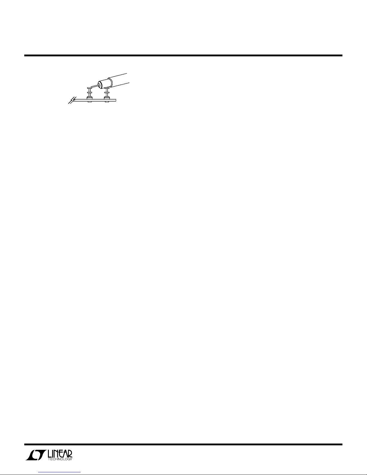
When verifying output ripple, it is important to
use the scope probe connection as shown in
figure 2.
Either regulator can be individually shut down
by moving jumpers JP7 or JP8 to the OFF position. Shutting down the Boost Converter
drops the converter’s output voltage to near
0V.
Jumpers JP7 and JP8 also can also be set for
regulator output voltage sequencing. Depending on the jumper setting, one of the regulators will remain shut down until the other regulator has reached regulation.
The linear regulator operation can be verified
by increasing the input supply voltage to 5V
and applying a suitable load on the VOUT
LDO terminal.
With JP1 in the Burst position, the converter
will operate in a low quiescent current burst
mode for light load current conditions and
switch to fixed frequency (PWM) operation
under heavier loads. In Burst mode, with light
loads, the output ripple voltage is higher than
in non-burst mode.
Applications requiring BURST mode operation
with input voltages below 1.2V, boosting to a
voltage between 4 and 5V out, may experience non-BURST mode operation at light load
conditions. This will result in higher light load
quiescent current. See data sheet curves
“Burst Mode Threshold Current vs VIN” for
additional information.
3
Page 4
QUICK START GUIDE FOR DEMONSTRATION CIRCUIT 1242A
600MA SYNCHRONOUS BOOST DC/DC CONVERTER AND 100MA LDO REGULATOR
See LTC3528 Data Sheet for additional information
V
Figure 2. Scope Probe Placement for
Measuring Output Ripple Voltage
OUT
GND
4
Page 5
QUICK START GUIDE FOR DEMONSTRATION CIRCUIT 1242A
600MA SYNCHRONOUS BOOST DC/DC CONVERTER AND 100MA LDO REGULATOR
5
Page 6

Mouser Electronics
Authorized Distributor
Click to View Pricing, Inventory, Delivery & Lifecycle Information:
Analog Devices Inc.:
DC1242A
 Loading...