

Page 1
LTC3417A-1
Dual Synchronous
1.5A/1A 4MHz Step-Down
DC/DC Regulator with POR
FEATURES
n
High Effi ciency: Up to 95%
n
1.5A/1A Guaranteed Minimum Output Current
n
Synchronizable to External Clock
n
Power-On-Reset Output
n
No Schottky Diodes Required
n
Programmable Frequency Operation: 1.5MHz or
Adjustable From 0.6MHz to 4MHz
n
Low Ripple (< 35mV
n
Low R
n
Short-Circuit Protected
n
VIN: 2.25V to 5.5V
n
Current Mode Operation for Excellent Line and Load
Internal Switches
DS(ON)
) BurstMode® Operation
P-P
Transient Response
n
125µA Quiescent Current in Sleep Mode
n
Ultralow Shutdown Current: IQ < 1µA
n
Low Dropout Operation: 100% Duty Cycle
n
Phase Pin Selects 2nd Channel Phase Relationship
with Respect to 1st Channel
n
Internal Soft-Start with Individual Run Pin Control
n
Available in Small Thermally Enhanced
(3mm × 5mm) DFN and 20-Lead TSSOP Packages
APPLICATIONS
n
GPS/Navigation Systems
n
Automotive Instrumentation
n
PC Cards
n
Industrial Power Supplies
n
General Purpose Point of Load DC/DC
DESCRIPTION
The LTC®3417A-1 is a dual constant frequency, synchronous step-down DC/DC converter. Intended for medium
power applications, it operates from a 2.25V to 5.5V input
voltage range and has a constant programmable switching
frequency, allowing the use of tiny, low cost capacitors
and inductors 2mm or less in height. Each output voltage
is adjustable from 0.8V to 5V. Internal synchronous, low
R
the need for external Schottky diodes.
The open drain POR pin goes low when either output
voltage falls 6% below regulation. The output will remain
low 150ms longer than the duration of the out of regulation condition.
A user selectable mode input allows the user to trade
off ripple voltage for light load effi ciency. Burst Mode
operation provides high effi ciency at light loads, while
pulse skip mode provides low ripple noise at light loads.
A phase mode pin allows the second channel to operate
in-phase or 180° out-of-phase with respect to channel 1.
Out-of-phase operation produces lower RMS current on
V
To further maximize battery life, the P-channel MOSFETs
are turned on continuously in dropout (100% duty cycle)
and both channels draw a total quiescent current of only
100µA. In shutdown, the device draws <1µA.
L, LT, LTC and LTM and Burst Mode are registered trademarks of Linear Technology
Corporation. All other trademarks are the property of their respective owners. Protected by U.S.
Patents including 5481178, 6580258, 6304066, 6127815, 6498466, 6611131, 6144194.
power switches provide high effi ciency without
DS(ON)
and thus lower stress on the input capacitor.
IN
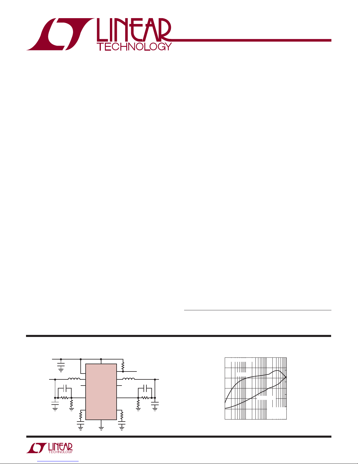
TYPICAL APPLICATION
V
IN
2.5V TO 5.5V
V
OUT1
1.8V
1.5A
47μF
10μF
1.5µH
22pF
V
IN
511k
412k
5.9k 2.87k
2200pF
FREQ
SW1
RUN1
V
FB1
I
TH1
V
IN
LTC3417A-1
GND
POR
SW2
RUN2
V
I
FB2
TH2
100k
2.2µH
V
IN
6800pF
3417A-1 TA01
412k
RESET
22pF
866k
V
2.5V
1A
22µF
OUT2
OUT2 Effi ciency
(Burst Mode Operation)
100
REFER TO FIGURE 4
95
EFFICIENCY
90
85
EFFICIENCY (%)
80
75
70
0.001
POWER LOSS
0.01 0.1 1
LOAD CURRENT (A)
VIN = 3.6V
= 2.5V
V
OUT
FREQ = 1MHz
3417A-1 TA01a
10
1
POWER LOSS (W)
0.1
0.01
0.001
0.0001
3417a1fa
1
Page 2
LTC3417A-1
ABSOLUTE MAXIMUM RATINGS
V
, V
IN1
Voltages ...................................... – 0.3V to 6V
IN2
SYNC/MODE, SW1, SW2, RUN1,
, V
RUN2, V
, I
I
TH1
TH2
– V
V
IN1
FB1
Voltages........ –0.3V to ((V
IN2
, PHASE, FREQ,
FB2
, V
– V
IN2
or V
IN1
.......................................... 0.3V
IN1
) + 0.3V)
IN2
PIN CONFIGURATION
TOP VIEW
1
RUN1
2
V
IN1
3
I
TH1
4
V
FB1
5
V
FB2
I
6
TH2
7
RUN2
8
V
IN2
16-LEAD (5mm × 3mm) PLASTIC DFN
EXPOSED PAD (PIN 17) IS PGND2/GNDD
DHC PACKAGE
T
= 125°C, θJA = 43°C/ W
JMAX
MUST BE SOLDERED TO PCB
16
PGND1
15
SW1
14
PHASE
13
12
11
10
9
GNDA
FREQ
POR
SW2
SYNC/MODE
17
(Note 1)
POR Voltage ................................................ –0.3V to 6V
Operating Temperature Range (Note 2)
LTC3417AE-1 ...................................... –40°C to 85°C
LTC3417AI-1 ..................................... –40°C to 125°C
Junction Temperature (Notes 7, 8) ...................... 125°C
Storage Temperature Range ...................–65°C to 150°C
TOP VIEW
1
GNDD
2
RUN1
3
V
IN1
4
I
TH1
5
V
FB1
V
FB2
I
TH2
RUN2
V
IN2
PGND2
20-LEAD PLASTIC TSSOP
T
JMAX
EXPOSED PAD (PIN 21) IS PGND2/GNDD
MUST BE SOLDERED TO PCB
21
6
7
8
9
10
FE PACKAGE
= 125°C, θJA = 38°C/ W
GNDD
20
PGND1
19
SW1
18
PHASE
17
GNDA
16
FREQ
15
POR
14
SW2
13
SYNC/MODE
12
PGND2
11
ORDER INFORMATION
LEAD FREE FINISH TAPE AND REEL PART MARKING* PACKAGE DESCRIPTION TEMPERATURE RANGE
LTC3417AEDHC-1#PBF LTC3417AEDHC-1#TRPBF 3417A1 16-Lead (3mm × 5mm) Plastic DFN –40°C to 85°C
LTC3417AIDHC-1#PBF LTC3417AIDHC-1#TRPBF 3417A1 16-Lead (3mm × 5mm) Plastic DFN –40°C to 125°C
LTC3417AEFE-1#PBF LTC3417AEFE-1#TRPBF LTC3417AFE-1 20-Lead Plastic TSSOP –40°C to 85°C
LTC3417AIFE-1#PBF LTC3417AIFE-1#TRPBF LTC3417AFE-1 20-Lead Plastic TSSOP –40°C to 125°C
Consult LTC Marketing for parts specifi ed with wider operating temperature ranges. *The temperature grade is identifi ed by a label on the shipping container.
Consult LTC Marketing for information on non-standard lead based fi nish parts.
For more information on lead free part marking, go to: http://www.linear.com/leadfree/
For more information on tape and reel specifi cations, go to: http://www.linear.com/tapeandreel/
The l denotes the specifi cations which apply over the full operating
ELECTRICAL CHARACTERISTICS
temperature range, otherwise specifi cations are at T
SYMBOL PARAMETER CONDITIONS MIN TYP MAX UNITS
V
I
IN1
FB1
, V
IN2
, I
FB2
Operating Voltage Range V
Feedback Pin Input Current VIN = 6V Pin Under Test = 3V ± 0.1 µA
2
= 25°C. VIN = 3.6V unless otherwise specifi ed (Note 2).
A
IN1
= V
IN2
2.25 5.5 V
3417a1fa
Page 3
LTC3417A-1
The l denotes the specifi cations which apply over the full operating
ELECTRICAL CHARACTERISTICS
temperature range, otherwise specifi cations are at T
SYMBOL PARAMETER CONDITIONS MIN TYP MAX UNITS
, V
V
FB1
FB2
ΔV
LINEREG
ΔV
LOADREG
g
m(EA)
I
S
I
S
f
OSC
I
LIM1
I
LIM2
R
DS(ON)1
R
DS(ON)2
I
SW1(LKG)
I
SW2(LKG)
V
UVLO
V
TH(POR)
R
POR
t
POR
V
RUN1, VRUN2
V
PHASE
I
RUN1, IRUN2, IPHASE,
I
SYNC/MODE
VTL
SYNC/MODE
VTH
SYNC/MODE
VTH
FREQ
Feedback Voltage (Note 3)
Reference Voltage Line Regulation. %/V
is the Percentage Change in V
Change in V
IN
OUT
Output Voltage Load Regulation I
Error Amplifi er Transconductance I
Input DC Supply Current (Note 4)
Active Mode V
Half Active Mode (V
Half Active Mode (V
= 0V, 1.5A Only) V
RUN2
= 0V, 1A Only) V
RUN1
Both Channels in Sleep Mode V
Shutdown V
Oscillator Frequency V
Peak Switch Current Limit on SW1 (1.5A) 2.1 2.5 A
Peak Switch Current Limit on SW2 (1A) 1.4 1.7 A
SW1 Top Switch On-Resistance (1.5A)
SW1 Bottom Switch On-Resistance
SW2 Top Switch On-Resistance (1A)
SW2 Bottom Switch On-Resistance
Switch Leakage Current SW1 (1.5A) V
Switch Leakage Current SW2 (1A) V
Undervoltage Lockout Threshold V
Power-On-Reset Threshold
Percentage Deviation of V
Voltage from
FB
Steady State Value (Typically 0.8V)
Power-On-Reset Pull Down On-Resistance 120 300
Power-On-Reset De-Assertion Delay from
Fault Removal
RUN1, RUN2 Threshold 0.3 0.85 1.5 V
PHASE Threshold High-CMOS Levels V
PHASE Threshold Low-CMOS Levels 0.5 V
RUN1, RUN2, PHASE and SYNC/MODE
Leakage Current
SYNC/MODE Threshold Voltage Low 0.5 V
SYNC/MODE Threshold Voltage High V
FREQ Threshold Voltage High V
= 25°C. VIN = 3.6V unless otherwise specifi ed (Note 2).
A
VIN = 2.25V to 5V (Note 3) 0.02 0.2 %/V
with a
, I
= 0.36V (Note 3)
TH1
TH2
I
, I
= 0.84V (Note 3)
TH1
TH2
, I
TH1
TH2(PINLOAD)
= V
FB1
FB2
V
= V
RUN1
= 0.75V, V
FB1
= 0.75V, V
FB2
= V
FB1
FB2
V
= V
RUN2
= V
RUN1
= V
FREQ
V
: RT = 143k
FREQ
V
: Resistor (Note 6)
FREQ
V
= 3.6V (Note 5)
IN1
V
= 3.6V (Note 5)
IN1
V
= 3.6V (Note 5)
IN2
V
= 3.6V (Note 5)
IN2
= 6V, V
IN1
= 6V, V
IN2
, V
IN1
IN2
V
, V
IN1
IN2
or V
V
FB1
FB2
or V
V
FB1
FB2
FREQ = V
= ±5µA (Note 3) 1400 µS
= 0.75V, V
RUN2
= 1V, V
IN
RUN2
IN
RUN1
RUN2
SYNC/MODE
= V
IN
SYNC/MODE
SYNC/MODE
SYNCMODE
= 0V 0.01 1 µA
= 0V 0.01 1 µA
= 0V 0.01 1 µA
= VIN, V
= VIN, V
= VIN, V
= VIN,
RUN1
RUN2
RUN1
= V
= V
IN
IN
=
Ramping Down
Ramping Up
Ramping Up –6 %
Ramping Down –8 %
IN
FREQ Tied to GND Through 143k Resistor 294,912 Clock
VIN = 6V, Pin Under Test = 3V ±0.01 ±1 µA
l
0.784 0.8 0.816 V
0.02
–0.02
–0.2
400 600 µA
260 400 µA
260 400 µA
125 250 µA
1.2
0.85
1.5
1
1.25
0.088
0.084
0.16
0.15
1.9
1.95
2.07
2.12
2.25
212,992 Clock
–0.5 V
IN
–0.5 V
IN
–0.5 V
IN
0.2
1.8
4
2.2
%
%
MHz
MHz
MHz
Cycles
Cycles
V
V
3417a1fa
3
Page 4
LTC3417A-1
ELECTRICAL CHARACTERISTICS
Note 1: Stresses beyond those listed under Absolute Maximum Ratings
may cause permanent damage to the device. Exposure to any Absolute
Maximum Rating condition for extended periods may affect device
reliability and lifetime.
Note 2: The LTC3417AE-1 is guaranteed to meet specifi ed performance
from 0°C to 85°C. Specifi cations over the –40°C to 85°C operating
ambient temperature range are assured by design, characterization
and correlation with statistical process controls. The LTC3417AI-1 is
guaranteed to meet performance specifi cations over the –40°C to 125°C
operating temperature range.
Note 3: The LTC3417A-1 is tested in feedback loop which servos V
the midpoint for the error amplifi er (V
for the error amplifi er (V
ITH2
= 0.6V).
= 0.6V) and V
ITH1
to the midpoint
FB2
FB1
to
Note 4: Total supply current is higher due to the internal gate charge being
Note 5: Switch on-resistance is guaranteed by design and test correlation
on the DHC package and by fi nal test correlation on the FE package.
Note 6: Variable frequency operation with resistor is guaranteed by design
but not production tested and is subject to duty cycle limitations.
Note 7: This IC includes overtemperature protection that is intended
to protect the device during momentary overload conditions. Junction
temperature will exceed 125°C when overtemperature protection is active.
Continuous operation above the specifi ed maximum operating junction
temperature may impair device reliability.
Note 8: T
J
dissipation, P
LTC3417AEDHC-1: T
LTC3417AEFE-1: T
delivered at the switching frequency.
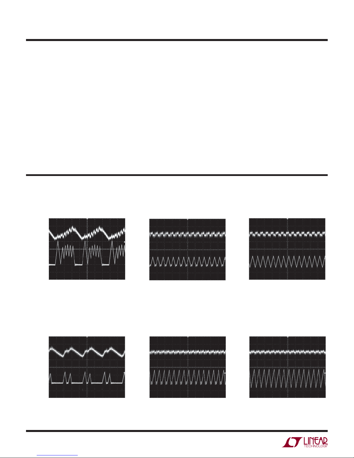
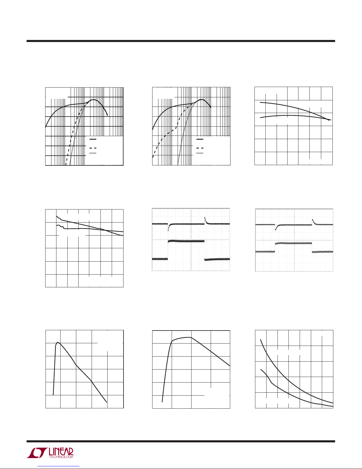
TYPICAL PERFORMANCE CHARACTERISTICS
OUT1 Pulse Skipping
Mode Operation
V
OUT
V
OUT
20mV/DIV
OUT1 Burst Mode Operation
20mV/DIV
is calculated from the ambient temperature, TA, and power
, according to the following formula:
D
= TA + (PD • 43°C/W)
J
= TA + (PD • 38°C/W)
J
OUT1 Forced Continuous
Mode Operation
V
OUT
20mV/DIV
250mA/DIV
V
OUT
20mV/DIV
250mA/DIV
I
L
VIN = 3.6V
= 1.8V
V
OUT
= 100mA
I
LOAD
REFER TO FIGURE 4
2µs/DIV
OUT2 Burst Mode Operation
I
L
VIN = 3.6V
= 2.5V
V
OUT
= 60mA
I
LOAD
REFER TO FIGURE 4
2µs/DIV
3417A-1 G01
3417A-1 G04
250mA/DIV
V
OUT
20mV/DIV
250mA/DIV
I
L
VIN = 3.6V
= 1.8V
V
OUT
= 100mA
I
LOAD
REFER TO FIGURE 4
2µs/DIV
OUT2 Pulse Skipping
Mode Operation
I
L
VIN = 3.6V
= 2.5V
V
OUT
= 60mA
I
LOAD
REFER TO FIGURE 4
2µs/DIV
3417A-1 G02
3417A-1 G05
250mA/DIV
V
20mV/DIV
250mA/DIV
I
L
VIN = 3.6V
= 1.8V
V
OUT
= 100mA
I
LOAD
REFER TO FIGURE 4
2µs/DIV
OUT2 Forced Continuous
Mode Operation
OUT
I
L
VIN = 3.6V
= 2.5V
V
OUT
= 60mA
I
LOAD
REFER TO FIGURE 4
2µs/DIV
3417A-1 G03
3417A-1 G06
3417a1fa
4
Page 5
TYPICAL PERFORMANCE CHARACTERISTICS
LTC3417A-1
OUT1 Effi ciency vs V
OUT1 Effi ciency vs Load Current
100
VIN = 2.5V
= 1.8V
V
OUT
95
90
85
80
75
EFFICIENCY (%)
70
65
60
0.001 0.1 1 10
REFER TO FIGURE 4
0.01
LOAD CURRENT (A)
OUT2 Effi ciency vs V
Burst Mode
OPERATION
PULSE SKIP
FORCED
CONTINUOUS
IN
3417A-1 G07
OUT2 Effi ciency vs Load Current
100
VIN = 3.6V
= 2.5V
V
OUT
95
90
85
80
75
EFFICIENCY (%)
70
65
60
0.001 0.1 1 100.01
REFER TO FIGURE 4
LOAD CURRENT (A)
Burst Mode
OPERATION
PULSE SKIP
FORCED
CONTINUOUS
3417A-1 G08
(Burst Mode Operation)
100
V
= 1.8V
OUT
95
90
85
EFFICIENCY (%)
80
75
70
2 2.5 3.5 4.5 5.5
(Pulse Skipping Mode) Load Step OUT1 Load Step OUT2
100
I
= 250mA
I
LOAD
LOAD
= 800mA
V
OUT1
100mV/DIV
V
OUT2
100mV/DIV
95
90
I
LOAD
3
IN
I
= 460mA
LOAD
= 1.4A
REFER TO FIGURE 4
45
VIN (V)
3417A-1 G09
85
EFFICIENCY (%)
80
75
70
2 2.5
3 3.5
V
= 2.5V
OUT
REFER TO FIGURE 4
4 4.5 5
VIN (V)
3417A-1 G10
I
OUT1
500mA/DIV
VIN = 3.6V
= 1.8V
V
OUT
= 0.25A to 1.4A
I
LOAD
REFER TO FIGURE 4
100µs/DIV
3417A-1 G11
Effi ciency vs Frequency OUT1 Effi ciency vs Frequency OUT2 R
94
92
90
88
EFFICIENCY (%)
86
84
82
0
TA = 27°C
= 3.6V
V
IN
= 1.8V
V
OUT
= 300mA
I
OUT
1234
FREQUENCY (MHz)
3417A-1 G13
5
90
85
80
75
EFFICIENCY (%)
70
65
60
0
TA = 27°C
= 3.6V
V
IN
= 2.5V
V
OUT
= 100mA
I
OUT
12 3
FREQUENCY (MHz)
3417A-1 G14
I
OUT2
500mA/DIV
0.105
0.100
0.095
(Ω)
DS(ON)
0.090
R
0.085
0.080
VIN = 3.6V
= 2.5V
V
OUT
= 0.25A to 0.8A
I
LOAD
REFER TO FIGURE 4
vs VIN OUT1
DS(ON)
P-CHANNEL SWITCH
N-CHANNEL SWITCH
2 2.5
3
100µs/DIV
4
3.5
VIN (V)
4.5
T
A =
3417A-1 G12
27°C
5
3417A-1 G15
5.5
3417a1fa
5
Page 6
LTC3417A-1
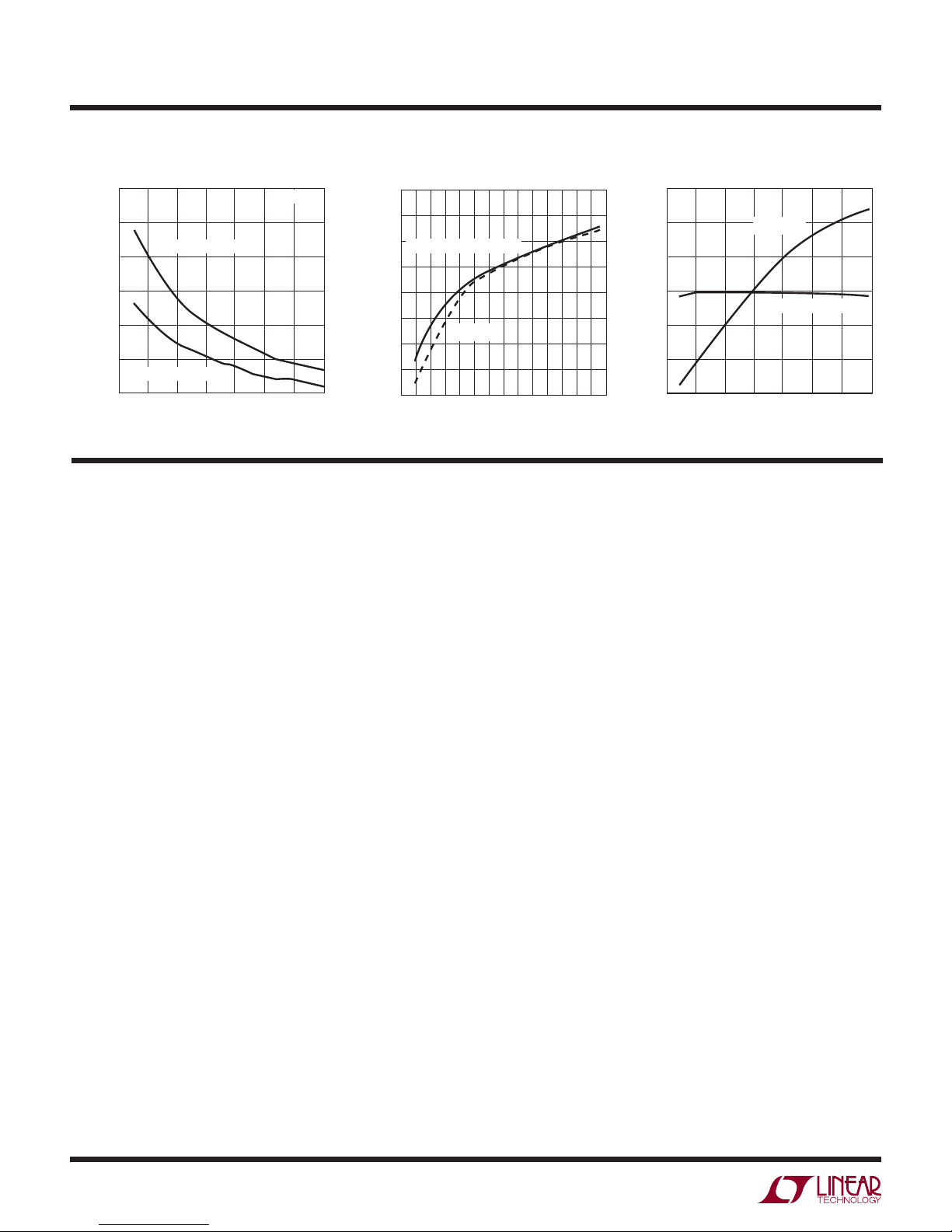
TYPICAL PERFORMANCE CHARACTERISTICS
R
0.20
0.19
0.18
(Ω)
0.17
DS(ON)
R
0.16
0.15
0.14
2
PIN FUNCTIONS
vs VIN OUT2 Frequency vs V
DS(ON)
P-CHANNEL SWITCH
N-CHANNEL SWITCH
2.5 3
4 5 5.5
3.5 4.5
VIN (V)
TA = 27°C
3417A-1 G16
6
4
2
FREQ = 143k TO GROUND
0
–2
–4
–6
FREQUENCY VARIATION (%)
–8
–10
2
(DFN/TSSOP)
FREQ = V
2.5 3
RUN1 (Pin 1/Pin 2): Enable for 1.5A Regulator. When
at Logic 1, 1.5A regulator is running. When at 0V, 1.5A
regulator is off. When both RUN1 and RUN2 are at 0V, the
part is in shutdown.
(Pin 2/Pin 3): Supply Pin for P-Channel Switch of
V
IN1
1.5A Regulator.
(Pin 3/Pin 4): Error Amplifi er Compensation Point
I
TH1
for 1.5A Regulator. The current comparator threshold
increases with this control voltage. Nominal voltage range
for this pin is 0V to 1.5V.
(Pin 4/Pin 5): Receives the feedback voltage from
V
FB1
external resistive divider across the 1.5A regulator output.
Nominal voltage for this pin is 0.8V.
(Pin 5/Pin 6): Receives the feedback voltage from
V
FB2
external resistive divider across the 1A regulator output.
Nominal voltage for this pin is 0.8V.
(Pin 6/Pin 7): Error Amplifi er Compensation Point for
I
TH2
1A regulator. The current comparator threshold increases
with this control voltage. Nominal voltage range for this
pin is 0V to 1.5V.
RUN2 (Pin 7/Pin 8): Enable for 1A Regulator. When at
Logic 1, 1A regulator is running. When at 0V, 1A regulator is off. When both RUN1 and RUN2 are at 0V, the part
is in shutdown.
(Pin 8/Pin 9): Supply Pin for P-Channel Switch of 1A
V
IN2
Regulator and Supply for Analog Circuitry.
Frequency vs Temperature
15
10
5
0
–5
FREQUENCY VARIATION (%)
–10
–15
–50
–25 0
25 75
TEMPERATURE (°C)
FREQ = V
IN
FREQ = 143k TO GROUND
50 100 125
3417A-1 G18
3.5
IN
IN
4 4.5
(V)
V
IN
5 5.5
3417A-1 G17
SYNC/MODE (Pin 9/Pin 12): Combination Mode Selection
and Oscillator Synchronization Pin. This pin controls the operation of the device. When the voltage on the SYNC/MODE
pin is >(V
– 0.5V), Burst Mode operation is selected.
IN
When the voltage on the SYNC/MODE pin is <0.5V, pulse
skipping mode is selected. When the SYNC/MODE pin is
held at V
/2, forced continuous mode is selected. The
IN
oscillation frequency can be synchronized to an external
oscillator applied to this pin. When synchronized to an
external clock, pulse skip mode is selected.
SW2 (Pin 10/Pin 13): Switch Node Connection to the
Inductor for the 1A Regulator. This pin swings from V
IN2
to PGND2.
POR (Pin 11/Pin 14): The Power-On-Reset Pin. This
open drain-logic output is pulled to GND when the output
voltage of either regulator falls 8% below regulation and
goes high approximately 150ms after both regulators are
above –6% of regulation. If either RUN1 or RUN2 is low
(the respective regulator is in sleep mode and therefore
the output voltage is low), then POR refl ects the regulation
of the running regulator.
FREQ (Pin 12/Pin 15): Frequency Set Pin. When FREQ is
, internal oscillator runs at 1.5MHz. When a resistor
at V
IN
is connected from this pin to ground, the internal oscillator
frequency can be varied from 0.6MHz to 4MHz.
GNDA (Pin 13/Pin 16): Analog Ground Pin for Internal
Analog Circuitry.
3417a1fa
6
Page 7

PIN FUNCTIONS
PHASE (Pin 14/Pin 17): Selects 1A regulator switching
phase with respect to 1.5A regulator switching. Set to
, the 1.5A regulator and the 1A regulator are in phase.
V
IN
When PHASE is at 0V, the 1.5A regulator and the 1A
regulator are switching 180 degrees out-of-phase. Do
not fl oat this pin.
SW1 (Pin 15/Pin 18): Switch Node Connection to the
Inductor for the 1.5A Regulator. This pin swings from
to PGND1.
V
IN1
FUNCTIONAL DIAGRAM
1.5A REGULATOR
V
FB1
0.752V
+
–
+
–
I
TH1
–
+
V
B
LTC3417A-1
PGND1 (Pin 16/Pin 19): Ground for SW1 N-Channel Driver.
PGND2, GNDD (Pins 1,10,11,20): TSSOP Package Only.
Ground for SW2 N-channel driver and digital ground for
circuit.
Exposed Pad (Pin 17/Pin 21): PGND2, GNDD. Ground for
SW2 N-channel driver and digital ground for circuit. The
Exposed Pad must be soldered to PCB ground.
V
I
TH
LIMIT
SLOPE
COMPENSATION
ANTI-SHOOT-
THROUGH
+
–
IN1
SW1
RUN1
VOLTAGE
REFERENCE
RUN2
SYNC/MODE
V
FB2
1A REGULATOR
0.848V
0.848V
0.752V
OSCILLATOR
ANTI-SHOOT-
THROUGH
SLOPE
+
–
–
DELAY
V
PGND1
PHASE
PGND2
IN2
FREQ
SW2
POR
3417A-1 BD
3417a1fa
+
+
–
–
+
–
+
+
–
V
IN2
–
+
–
+
–
+
+
V
B
–
I
TH2
LOGIC
LOGIC
I
LIMIT
COMPENSATION
TH
7
Page 8

LTC3417A-1
OPERATION
The LTC3417A-1 uses a constant frequency, current
mode architecture. Both channels share the same clock
frequency. The PHASE pin sets whether the channels are
running in-phase or out of phase. The operating frequency
is determined by connecting the FREQ pin to V
for
IN
1.5MHz operation or by connecting a resistor from FREQ
to ground for a frequency from 0.6MHz to 4MHz. To suit
a variety of applications, the SYNC/MODE pin allows the
user to trade off noise for effi ciency.
The output voltages are set by external dividers returned
to the V
FB1
and V
pins. An error amplifi er compares the
FB2
divided output voltage with a reference voltage of 0.8V and
adjusts the peak inductor current accordingly. Undervoltage
comparators will pull the POR output low when either output
voltage is 8% below its targeted value. The POR output
will go high after 212,992 cycles (when FREQ is high) or
294,912 cycles (when FREQ is tied to ground through an
external resistor), or about 150ms, after both regulators
are above -6% of the target output voltage.
Main Control Loop
For each regulator, during normal operation, the P-channel MOSFET power switch is turned on at the beginning
of a clock cycle when the V
voltage is below the refer-
FB
ence voltage. The current into the inductor and the load
increases until the current limit is reached. The switch
turns off and energy stored in the inductor fl ows through
the bottom N-channel MOSFET switch into the load until
the next clock cycle.
The peak inductor current is controlled by the voltage
on the I
This amplifi er compares the V
When the load current increases the V
pin, which is the output of the error amplifi er.
TH
pin to the 0.8V reference.
FB
voltage decreases
FB
slightly below the reference. This decrease causes the error amplifi er to increase the I
voltage until the average
TH
inductor current matches the new load current.
Low Current Operation
Three modes are available to control the operation of the
LTC3417A-1 at low currents. Each of the three modes
automatically switch from continuous operation to the
selected mode when the load current is low.
To optimize effi ciency, Burst Mode operation can be selected. When the load is relatively light, the LTC3417A-1
automatically switches into Burst Mode operation in which
the PMOS switches operate intermittently based on load
demand. By running cycles periodically, the switching
losses, which are dominated by the gate charge losses
of the power MOSFETs, are minimized. The main control
loop is interrupted when the output voltage reaches the
desired regulated value. The hysteresis voltage comparator
trips when I
is below 0.24V, shutting off the switch and
TH
reducing the power. The output capacitor and the inductor supply the power to the load until I
exceeds 0.31V,
TH
turning on the switch and the main control loop which
starts another cycle.
For lower output voltage ripple at low currents, pulse skipping mode can be used. In this mode, the LTC3417A-1
continues to switch at constant frequency down to very
low currents, where it will begin skipping pulses used to
control the power MOSFETs.
Finally, in forced continuous mode, the inductor current is
constantly cycled creating a fi xed output voltage ripple at all
output current levels. This feature is desirable in telecommunications since the noise is a constant frequency and is
thus easy to fi lter out. Another advantage of this mode is
that the regulator is capable of both sourcing current into
a load and sinking some current from the output.
The mode selection for the LTC3417A-1 is set using the
SYNC/MODE pin. The SYNC/MODE pin sets the mode for
both the1A and the 1.5A step-down DC/DC converters.
The main control loop is shut down by pulling the RUN pin
to ground. A digital soft-start is enabled after shutdown,
which will slowly ramp the peak inductor current up over
1024 clock cycles.
8
3417a1fa
Page 9

OPERATION
LTC3417A-1
Dropout Operation
When the input supply voltage decreases toward the output
voltage, the duty cycle increases to 100%. In this dropout
condition, the PMOS switch is turned on continuously with
the output voltage being equal to the input voltage minus
the voltage drops across the internal P-channel MOSFET
and inductor.
APPLICATIONS INFORMATION
A general LTC3417A-1 application circuit is shown in
Figure 4. External component selection is driven by the
load requirement, and begins with the selection of the
inductors L1 and L2. Once L1 and L2 are chosen, C
C
OUT1
and C
can be selected.
OUT2
Operating Frequency
Selection of the operating frequency is a tradeoff between
effi ciency and component size. High frequency operation
allows the use of smaller inductor and capacitor values.
Operation at lower frequencies improves effi ciency by
reducing internal gate charge losses but requires larger
inductance values and/or capacitance to maintain low
output ripple voltage.
The operating frequency, f
mined by pulling the FREQ pin to V
, of the LTC3417A-1 is deter-
O
for 1.5MHz opera-
IN
tion or by connecting an external resistor from FREQ to
ground. The value of the resistor sets the ramp current
that is used to charge and discharge an internal timing
capacitor within the oscillator and can be calculated by
using the following equation:
RT≈
1.61• 10
f
O
11
Ω
()
– 16.586kΩ
for 0.6MHz ≤ fO ≤ 4MHz. Alternatively, use Figure 1 to
select the value for R
.
T
The maximum operating frequency is also constrained
by the minimum on-time and duty cycle. This can be
calculated as:
IN
,
Low Supply Operation
The LTC3417A-1 incorporates an undervoltage lockout
circuit which shuts down the part when the input voltage
drops below about 2.07V to prevent unstable operation.
160
140
120
100
80
(kΩ)
T
R
60
40
20
0
f
O(MAX)
0.5 1.0 2.0
0
6.67
1.5 2.5 3.53.0 4.0
FREQUENCY (MHz)
Figure 1. Frequency vs R
V
OUT
V
IN(MAX)
MHz
()
4.5
3417A-1 F01
T
The minimum frequency is limited by leakage and noise
coupling due to the large resistance of R
.
T
Inductor Selection
Although the inductor does not infl uence the operating
frequency, the inductor value has a direct effect on ripple
current. The inductor ripple current, ΔI
higher inductance and increases with higher V
.
V
OUT
V
I
OUT
=
L
fO•L
1–
V
OUT
V
IN
, decreases with
L
or
IN
Accepting larger values of ΔIL allows the use of low inductances, but results in higher output voltage ripple, greater
core losses and lower output current capability.
3417a1fa
9
Page 10

LTC3417A-1
APPLICATIONS INFORMATION
A reasonable starting point for setting ripple current is
= 0.35I
ΔI
L
LOAD(MAX)
current output. The largest ripple, ΔI
, where I
LOAD(MAX)
, occurs at the maxi-
L
is the maximum
mum input voltage. To guarantee that the ripple current
stays below a specifi ed maximum, the inductor value
should be chosen according to the following equation:
V
OUT
L =
fO• I
L
V
1–
V
IN(MAX)
OUT
The inductor value will also have an effect on Burst Mode
operation. The transition from low current operation begins
when the peak inductor current falls below a level set by the
burst clamp. Lower inductor values result in higher ripple
current which causes this to occur at lower load currents.
This causes a dip in effi ciency in the upper range of low
current operation. In Burst Mode operation, lower inductor
values will cause the burst frequency to increase.
Inductor Core Selection
Different core materials and shapes will change the size/
current relationship of an inductor. Toroid or shielded
pot cores in ferrite or permalloy materials are small and
don’t radiate much energy, but generally cost more than
powdered iron core inductors with similar electrical
characteristics. The choice of which style inductor to use
often depends more on the price vs size requirements
of any radiated fi eld/EMI requirements than on what the
LTC3417A-1 requires to operate. Table 1 shows some
typical surface mount inductors that work well in
LTC3417A-1 applications.
Input Capacitor (C
) Selection
IN
In continuous mode, the input current of the converter can
be approximated by the sum of two square waves with
duty cycles of approximately V
OUT1/VIN
and V
OUT2/VIN
. To
prevent large voltage transients, a low equivalent series
resistance (ESR) input capacitor sized for the maximum
RMS current must be used. Some capacitors have a
de-rating spec for maximum RMS current. If the capacitor being used has this requirement, it is necessary to
calculate the maximum RMS current. The RMS current
calculation is different if the part is used in “in phase” or
“out of phase”.
For “in phase”, there are two different equations:
> V
V
OUT1
I
= 2•I1•I2•D2(1–D1)+I
RMS
V
> V
OUT2
I
= 2•I1•I2•D1(1–D2)+I
RMS
OUT2
OUT1
:
2
(D2 – D22)+I
2
2
(D1– D12)
1
:
2
(D2 – D22)+I
2
2
(D1– D12)
1
where:
V
OUT1
D1=
V
IN
and D2 =
V
OUT2
V
IN
Table 1
MANUFACTURER PART NUMBER VALUE (μH) MAX DC CURRENT (A) DCR DIMENSIONS L × W × H (mm)
L1 on OT1
Toko A920CY-1R5M-D62CB
A918CY-1R5M-D62LCB
Coilcraft D01608C-152ML 1.5 2.6 0.06 6.6 × 4.5 × 2.9
Sumida CDRH4D22/HP 1R5 1.5 3.9 0.031 5 × 5 × 2.4
Midcom DUP-1813-1R4R 1.4 5.5 0.033 4.3 × 4.8 × 3.5
L2 on OUT2
Toko A915AY-2ROM-D53LC 2.0 3.9 0.027 5 × 5 × 3
Coilcraft D01608C-222ML 2.2 2.3 0.07 6.6 × 4.5 × 2.9
Sumida CDRH3D16/HP 2R2 2.2
Midcom DUP-1813-2R2R 2.2 3.9 0.047 4.3 × 4.8 × 3.5
10
1.5
1.5
2.2
2.8
2.9
1.75
1.6
0.014
0.018
0.047
0.035
6 × 6 × 2.5
6 × 6 × 2
4 × 4 × 1.8
3.2 × 3.2 × 2
3417a1fa
Page 11

APPLICATIONS INFORMATION
LTC3417A-1
When D1 = D2 then the equation simplifi es to:
I
= I1+I
()
RMS
D1–D
()
2
or
V
()
I
= I1+I
()
RMS
OUTVIN–VOUT
2
V
IN
where the maximum average output currents I1 and I2
equal the respective peak currents minus half the peakto-peak ripple currents:
ΔI
I1=I
LIM1
I2=I
LIM2
These formula have a maximum at V
= (I1 + I2)/2. This simple worst case is commonly
I
RMS
used to determine the highest I
L1
–
2
ΔI
L2
–
2
RMS
= 2V
IN
.
, where
OUT
For “out of phase” operation, the ripple current can be
lower than the “in phase” current.
In the “out of phase” case, the maximum I
occur when V
curs when V
= V
OUT1
OUT1
. As a good rule of thumb, the amount of worst
= V
OUT1
– VIN/2 = V
. The maximum typically oc-
OUT2
or when V
OUT2
does not
RMS
OUT2
– VIN/2
case ripple is about 75% of the worst case ripple in the
“in phase” mode. Also note that when V
/2 and I1 = I2, the ripple is zero.
V
IN
OUT1
= V
OUT2
=
Note that capacitor manufacturer’s ripple current ratings
are often based on only 2000 hours lifetime. This makes
it advisable to further derate the capacitor, or choose a
capacitor rated at a higher temperature than required.
Several capacitors may also be paralleled to meet the
size or height requirements of the design. An additional
0.1µF to 1µF ceramic capacitor is also recommended on
for high frequency decoupling, when not using an all
V
IN
ceramic capacitor solution.
Output Capacitor (C
The selection of C
OUT1
OUT1
and C
and C
OUT2
) Selection
OUT2
is driven by the required
ESR to minimize voltage ripple and load step transients.
Typically, once the ESR requirement is satisfi ed, the
capacitance is adequate for fi ltering. The output ripple
(ΔV
where fO = operating frequency, C
and ΔI
is highest at maximum input voltage, since ΔI
with input voltage. With ΔI
ripple will be less than 100mV at maximum V
) is determined by:
OUT
V
ILESR
OUT
= ripple current in the inductor. The output ripple
L
COUT
+
= 0.35I
L
1
8•fO•C
OUT
OUT
= output capacitance
increases
L
LOAD(MAX)
, the output
IN
and fO =
1MHz with:
ESR
Once the ESR requirements for C
RMS current rating generally far exceeds the I
< 150m
COUT
have been met, the
OUT
RIPPLE(P-P)
requirement, except for an all ceramic solution.
In surface mount applications, multiple capacitors may
have to be paralleled to meet the capacitance, ESR or RMS
current handling requirement of the application. Aluminum
electrolytic, special polymer, ceramic and dry tantalum
capacitors are all available in surface mount packages. The
OS-CON semiconductor dielectric capacitor available from
Sanyo has the lowest ESR(size) product of any aluminum
electrolytic at a somewhat higher price. Special polymer
capacitors, such as Sanyo POSCAP, offer very low ESR, but
have a lower capacitance density than other types. Tantalum
capacitors have the highest capacitance density, but it has
a larger ESR and it is critical that the capacitors are surge
tested for use in switching power supplies. An excellent
choice is the AVX TPS series of surface tantalums, available
in case heights ranging from 2mm to 4mm. Aluminum
electrolytic capacitors have a signifi cantly larger ESR, and
are often used in extremely cost-sensitive applications
provided that consideration is given to ripple current
ratings and long term reliability. Ceramic capacitors have
the lowest ESR and cost but also have the lowest capacitance density, high voltage and temperature coeffi cient
and exhibit audible piezoelectric effects. In addition, the
high Q of ceramic capacitors along with trace inductance
can lead to signifi cant ringing. Other capacitor types
include the Panasonic specialty polymer (SP) capacitors.
3417a1fa
11
Page 12

LTC3417A-1
APPLICATIONS INFORMATION
In most cases, 0.1µF to 1µF of ceramic capacitors should
also be placed close to the LTC3417A-1 in parallel with
the main capacitors for high frequency decoupling.
Ceramic Input and Output Capacitors
Higher value, lower cost ceramic capacitors are now
becoming available in smaller case sizes. Because the
LTC3417 control loop does not depend on the output
capacitor’s ESR for stable operation, ceramic capacitors
can be used freely to achieve very low output ripple and
small circuit size. When choosing the input and output
ceramic capacitors, choose the X5R or X7R dielectric
formulations. These dielectrics have the best temperature
and voltage characteristics of all the ceramics for a given
value and size.
Great care must be taken when using only ceramic input
and output capacitors. When a ceramic capacitor is used
at the input and the power is being supplied through long
wires, such as from a wall adapter, a load step at the output
can induce ringing at the V
pin. At best, this ringing can
IN
couple to the output and be mistaken as loop instability.
At worst, the ringing at the input can be large enough to
damage the part.
Since the ESR of a ceramic capacitor is so low, the input
and output capacitor must fulfi ll a charge storage requirement. During a load step, the output capacitor must
instantaneously supply the current to support the load
until the feedback loop raises the switch current enough
to support the load. The time required for the feedback
loop to respond is dependent on the compensation components and the output capacitor size. Typically, 3 to 4
cycles are required to respond to a load step, but only in
the fi rst cycle does the output drop linearly. The output
droop, V
, is usually about 2 to 3 times the linear
DROOP
droop of the fi rst cycle. Thus, a good place to start is with
the output capacitor size of approximately:
ΔI
C
≈ 2.5
OUT
fO•V
OUT
DROOP
More capacitance may be required depending on the duty
cycle and load step requirements.
In most applications, the input capacitor is merely required
to supply high frequency bypassing, since the impedance
to the supply is very low. A 10µF ceramic capacitor is
usually enough for these conditions.
Setting the Output Voltage
The LTC3417A-1 develops a 0.8V reference voltage between
the feedback pins, V
FB1
and V
, and the signal ground
FB2
as shown in Figure 4. The output voltages are set by two
resistive dividers according to the following formulas:
V
OUT1
V
OUT2
0.8V 1+
0.8V 1+
R2
R3
R4
R1
Keeping the current small (<5µA) in these resistors
maximizes effi ciency, but making the current too small
may allow stray capacitance to cause noise problems and
reduce the phase margin of the error amp loop.
To improve the frequency response, a feed-forward capacitor, C
to route the V
, may also be used. Great care should be taken
F
node away from noise sources, such as
FB
the inductor or the SW line.
Power-On Reset
The POR pin is an open-drain output which pulls low when
either regulator is out of regulation. When both output
voltages are above –6% of regulation, a timer is started
which allows the POR output to go high after 212,992
clock cycles (when FREQ is tied to V
) or 294,912 clock
IN
cycles (when FREQ is tied to ground through an external
resistor). This results in a delay of approximately 150ms
when the oscillator is set to 2MHz. When either channel
is shut down, the POR output refl ects the condition of the
running regulator.
12
3417a1fa
Page 13

APPLICATIONS INFORMATION
LTC3417A-1
V
RUN
2V/DIV
V
OUT
1V/DIV
I
L
1A/DIV
VIN = 3.6V
= 1.8V
V
OUT
= 0.9Ω
R
L
Figure 2. Digital Soft-Start OUT1
200µs/DIV
3417A-1 F02
Soft-Start
Soft-start reduces surge currents from V
by gradu-
IN
ally increasing the peak inductor current. Power supply
sequencing can also be accomplished by controlling the
pin. The LTC3417A-1 has an internal digital soft-start
I
TH
for each regulator output, which steps up a clamp on
over 1024 clock cycles, as can be seen in Figures 2
I
TH
and 3. As the voltage on I
ramps through its operating
TH
range, the internal peak current limit is also ramped at a
proportional linear rate.
Mode Selection
The SYNC/MODE pin is a multipurpose pin which provides
mode selection and frequency synchronization. Connecting this pin to V
enables Burst Mode operation for both
IN
regulators, which provides the best low current effi ciency
at the cost of a higher output voltage ripple. When SYNC/
MODE is connected to ground, pulse skipping operation
is selected for both regulators, which provides the lowest output voltage and current ripple at the cost of low
current effi ciency. Applying a voltage that is more than
1V from either supply results in forced continuous mode
for both regulators, which creates a fi xed output ripple
and allows the sinking of some current (about 1/2ΔI
).
L
Since the switching noise is constant in this mode, it is
also the easiest to fi lter out. In many cases, the output
voltage can be simply connected to the SYNC/MODE pin,
selecting the forced continuous mode except at start-up.
The LTC3417A-1 can be synchronized to an external clock
signal by the SYNC/MODE pin. The internal oscillator frequency should be set to 20% lower than the external clock
frequency to ensure adequate slope compensation, since
slope compensation is derived from the internal oscillator.
During synchronization, the mode is set to pulse skipping
and the top switch turn-on is synchronized to the rising
edge of the external clock.
When using an external clock, with the PHASE pin low, the
switching of the two channels occur at the edges of the
external clock. A 50% duty cycle will therefore produce
180° out-of-phase operation.
Checking Transient Response
The I
pin compensation allows the transient response
TH
to be optimized for a wide range of loads and output
capacitors. The availability of the I
pin not only allows
TH
optimization of the control loop behavior, but also provides a DC coupled and AC fi lited closed-loop response
test point. The DC step, rise time, and settling at this test
point truly refl ects the closed-loop response. Assuming a
predominantly second order system, phase margin and/or
or damping factor can be estimated using the percentage
of overshoot seen at this pin. The bandwidth can also be
estimated using the percentage of overshoot seen at this
pin or by examining the rise time at this pin.
V
RUN
2V/DIV
V
OUT
1V/DIV
I
L
0.5A/DIV
VIN = 3.6V
= 2.5V
V
OUT
= 2Ω
R
L
Figure 3. Digital Soft-Start OUT2
200µs/DIV
3417A-1 F03
3417a1fa
13
Page 14

LTC3417A-1
APPLICATIONS INFORMATION
The ITH external components shown in the Figure 4 circuit
will provide an adequate starting point for most applications. The series RC fi lter sets the dominant pole-zero
loop compensation. The values can be modifi ed slightly
(from 0.5 to 2 times their suggested values) to optimize
transient response once the fi nal PC layout is done and
the particular output capacitor type and value have been
determined. The output capacitors need to be selected
because of various types and values determine the loop
feedback factor gain and phase. An output current pulse
of 20% to 100% of full load current having a rise time
of 1µs to 10µs will produce output voltage and I
TH
pin
waveforms that will give a sense of overall loop stability
without breaking the feedback loop.
Switching regulators take several cycles to respond to a
step in load current. When a load step occurs, V
mediately shifts by an amount equal to ΔI
where ESR
ΔI
also begins to charge or discharge C
LOAD
is the effective series resistance of C
COUT
LOAD
OUT
OUT
• ESR
COUT
generat-
im-
OUT
,
.
ing a feedback error signal used by the regulator to return
to its steady-state value. During this recovery time,
V
OUT
can be monitored for overshoot or ringing that would
V
OUT
indicate a stability problem.
The initial output voltage step may not be within the bandwidth of the feedback loop, so the standard second order
overshoot/DC ratio cannot be used to determine phase
margin. The gain of the loop increases with R
bandwidth of the loop increases with decreasing C
is increased by the same factor that C
R
ITH
ITH
and the
ITH
. If
ITH
is decreased,
the zero frequency will be kept the same, thereby keeping
the phase the same in the most critical frequency range
of the feedback loop. In addition, feedforward capacitors,
C1 and C2, can be added to improve the high frequency
response, as shown in Figure 4. Capacitor C1 provides
phase lead by creating a high frequency zero with R1
which improves the phase margin for the 1.5A SW1 channel. Capacitor C2 provides phase lead by creating a high
frequency zero with R3 which improves the phase margin
for the 1A SW2 channel.
The output voltage settling behavior is related to the stability
of the closed-loop system and will demonstrate the actual
overall supply performance. For a detailed explanation of
optimizing the compensation components, including a
review of control loop theory, refer to Linear Technology
Application Note 76.
Although a buck regulator is capable of providing the full
output current in dropout, it should be noted that as the
input voltage V
drops toward V
IN
, the load step capability
OUT
does decrease due to the decreasing voltage across the
inductor. Applications that require large load step capability near dropout should use a different topology such as
SEPIC, Zeta, or single inductor, positive buck boost.
In some applications, a more severe transient can be
caused by switching in loads with large (>1µF) input capacitors. The discharged input capacitors are effectively
put in parallel with C
, causing a rapid drop in V
OUT
OUT
. No
regulator can deliver enough current to prevent this problem, if the switch connecting the load has low resistance
and is driven quickly. The solution is to limit the turn-on
speed of the load switch driver. A Hot Swap™ controller
is designed specifi cally for this purpose and usually incorporates current limiting, short-circuit protection, and
soft- starting.
Effi ciency Considerations
The percent effi ciency of a switching regulator is equal to
the output power divided by the input power times 100.
It is often useful to analyze individual losses to determine
what is limiting the effi ciency and which change would
produce the most improvement. Percent effi ciency can
be expressed as:
% Effi ciency = 100% – (P1+ P2 + P3 +…)
where P1, P2, etc. are the individual losses as a percentage of input power.
14
Hot Swap is a trademark of Linear Technology Corporation.
3417a1fa
Page 15

APPLICATIONS INFORMATION
LTC3417A-1
Although all dissipative elements in the circuit produce
losses, four main sources account for most of the losses
in LTC3417A-1 circuits: 1) LTC3417A-1 I
2
switching losses, 3) I
1) The I
current is the DC supply current given in the elec-
S
R losses, 4) other losses.
current, 2)
S
trical characteristics which excludes MOSFET driver and
control currents. I
loss that increases with V
current results in a small (<0.1%)
S
, even at no load.
IN
2) The switching current is the sum of the MOSFET driver
and control currents. The MOSFET driver current results from switching the gate capacitance of the power
MOSFETs. Each time a MOSFET gate is switched from
low to high to low again, a packet of charge moves from
to ground. The resulting charge over the switching
V
IN
period is a current out of V
that is typically much larger
IN
than the DC bias current. The gate charge losses are
proportional to V
and thus their effects will be more
IN
pronounced at higher supply voltages.
2
R losses are calculated from the DC resistances of the
3) I
internal switches, R
, and the external inductor, RL. In
SW
continuous mode, the average output current fl owing
through inductor L is “chopped” between the internal
top and bottom switches. Thus, the series resistance
looking into the SW pin is a function of both top and
bottom MOSFET R
and the duty cycle (DC) as
DS(ON)
follows:
R
SW
The R
= (R
DS(ON)
TOP)(DC) + (R
DS(ON)
DS(ON)
BOT)(1 – DC)
for both the top and bottom MOSFETs can be
obtained from the Typical Performance Characteristics
2
2
(R
R losses:
+ RL)
SW
curves. Thus, to obtain I
2
I
R losses = I
where R
OUT
is the resistance of the inductor.
L
4) Other “hidden” losses such as copper trace and internal
battery resistances can account for additional effi ciency
degradations in portable systems. It is very important
to include these “system” level losses in the design
of a system. The internal battery and fuse resistance
losses can be minimized by making sure that C
adequate charge storage and very low ESR
IN
COUT
has
at
the switching frequency. Other losses including diode
conduction losses during dead-time and inductor core
losses generally account for less than 2% total additional
loss.
Thermal Considerations
The LTC3417A-1 requires the package Exposed Pad
(PGND2/GNDD pin) to be well soldered to the PC board.
This gives the DFN and TSSOP packages exceptional
thermal properties, compared to similar packages of this
size, making it diffi cult in normal operation to exceed the
maximum junction temperature of the part. In a majority
of applications, the LTC3417A-1 does not dissipate much
heat due to its high effi ciency. However, in applications
where the LTC3417A-1 is running at high ambient temperature with low supply voltage and high duty cycles,
such as in dropout, the heat dissipated may exceed the
maximum junction temperature of the part. If the junction
temperature reaches approximately 150°C, both switches
in both regulators will be turned off and the SW nodes will
become high impedance.
To prevent the LTC3417A-1 from exceeding its maximum
junction temperature, the user will need to do some thermal
analysis. The goal of the thermal analysis is to determine
whether the power dissipated exceeds the maximum
junction temperature of the part. The temperature rise is
given by:
RISE
= PD • θ
JA
T
where PD is the power dissipated by the regulator and θJA
is the thermal resistance from the junction of the die to
the ambient temperature.
The junction temperature, T
T
J
= T
RISE
+ T
AMBIENT
, is given by:
J
As an example, consider the case when the LTC3417A-1
is in dropout in both regulators at an input voltage of 3.3V
with load currents of 1.5A and 1A. From the Typical Performance Characteristics graph of Switch Resistance, the
R
and the R
resistance of the 1.5A P-channel switch is 0.09
DS(ON)
of the 1A P-channel switch is 0.163.
DS(ON)
3417a1fa
15
Page 16

LTC3417A-1
APPLICATIONS INFORMATION
The power dissipated by the part is:
PD = I
1
2
• R
DS(ON)1
+ I
2
2
• R
DS(ON)2
PD = 1.52 • 0.09 + 12 • 0.163
PD = 366mW
The DFN package junction-to-ambient thermal resistance,
, is about 43°C/W. Therefore, the junction temperature
θ
JA
of the regulator operating in a 70°C ambient temperature
is approximately:
= 0.366 • 43 + 70
T
J
= 85.7°C
T
J
Remembering that the above junction temperature is
obtained from an R
the junction temperature based on a higher R
at 25°C, we might recalculate
DS(ON)
DS(ON)
since
it increases with temperature. However, we can safely assume that the actual junction temperature will not exceed
the absolute maximum junction temperature of 125°C.
Design Example
As a design example, consider using the LTC3417A-1 in
a portable application with a Li-Ion battery. The battery
provides a V
from 2.8V to 4.2V. One load requires 1.8V
IN
at 1.5A in active mode, and 1mA in standby mode. The
other load requires 2.5V at 1A in active mode, and 500µA
in standby mode. Since both loads still need power in
standby, Burst Mode operation is selected for good low
load effi ciency (SYNC/MODE = V
IN
).
First, determine what frequency should be used. Higher
frequency results in a lower inductor value for a given ΔI
is estimated as 0.35I
(ΔI
L
LOAD(MAX)
). Reasonable values
L
for wire wound surface mount inductors are usually in the
range of 1µH to 10µH.
CONVERTER OUTPUT I
SW1 1.5A 525mA
SW2 1A 350mA
LOAD(MAX)
ΔI
L
Using the 1.5MHz frequency setting (FREQ = V
), we get
IN
the following equations for L1 and L2:
L1=
1.5MHz • 525mA
1.8V
1.8V
1–
4.2V
= 1.3μH
Use 1.5μH.
L2=
1.5MHz • 350m
2.5V
A
2.5V
1–
4.2V
= 1.9μH
Use 2.2μH.
C
selection is based on load step droop instead of ESR
OUT
requirements. For a 2.5% output droop:
C
= 2.5 •
OUT1
OUT2
= 2.5 •
C
1.5MHz 5% •1.8V
1.5MHz 5% • 2.5V
1.5A
= 28μF
()
1A
= 13μF
()
The closest standard values are 47µF and 22µF.
The output voltages can now be programmed by choosing the values of R1, R2, R3, and R4. To maintain high
effi ciency, the current in these resistors should be kept
small. Choosing 2µA with the 0.8V feedback voltages makes
R2 and R4 equal to 400k. A close standard 1% resistor is
412k. This then makes R1 = 515k. A close standard 1%
is 511k. Similarily, with R4 at 412k, R3 is equal to 875k.
A close 1% resistor is 866k.
The compensation should be optimized for these components by examining the load step response, but a good
place to start for the LTC3417A-1 is with a 5.9k and
2200pF fi lter on I
and 2.87k and 6800pF on I
TH1
TH2
. The
output capacitor may need to be increased depending on
the actual undershoot during a load step.
The POR pin is an open drain output and requires a pullup resistor. A 100k resistor is used for adequate speed.
Figure 4 shows a complete schematic for this design.
16
3417a1fa
Page 17

APPLICATIONS INFORMATION
V
IN
C1 22pF
R1 511k
C
IN
10µF
L1
1.5µH
R2
412k
2200pF
5.9k
C3
V
IN
R5
V
C
OUT1
47µF
OUT1
1.8V
1.5A
2.25V TO 5.5V
C
IN1
0.1µF
SYNC/MODE
SW1
RUN1
V
PHASE
I
GNDA
V
LTC3417A-1
FB1
TH1
V
IN1
IN2
EXPOSED
PAD GNDD
POR
SW2
RUN2
V
FB2
FREQ
I
TH2
C
IN2
0.1µF
V
V
R7
100k
IN
IN
R6
2.87k
RESET
L2
2.2µH
412k
C4
6800pF
3417A-1 F04
LTC3417A-1
V
OUT2
C2 22pF
R3 866k
R4
2.5V
1A
C
OUT2
22µF
L1: MIDCOM DUS-5121-1R5R
: KEMET C1210C226K8PAC
C
OUT1
100
95
90
85
EFFICIENCY (%)
80
75
70
0.001 0.1 1 10
Figure 4. 1.8V at 1.5A/2.5V at 1A Step-Down Regulators
L2: MIDCOM DUS-5121-2R2R
C
, CIN: KEMET C1206C106K4PAC
OUT2
OUT1 Effi ciency vs Load Current
VIN = 3.6V
= 1.8V
V
OUT
FREQ = 1MHz
REFER TO FIGURE 4
EFFICIENCY
POWER LOSS
0.01
LOAD CURRENT (A)
3417A-1 F04a
10
1
POWER LOSS (W)
0.1
0.01
0.001
3417a1fa
17
Page 18

LTC3417A-1
APPLICATIONS INFORMATION
Board Layout Considerations
When laying out the printed circuit board, the following
checklist should be used to ensure proper operation of the
LTC3417A-1. These items are also illustrated graphically
in the layout diagram of Figure 5. Check the following in
your layout.
. Does the capacitor CIN connect to the power V
1
(Pin 2), V
(Pin 8), and PGND2/GNDD (Pin 17) as
IN2
IN1
close as possible (DFN package)? It may be necessary
to split C
into two capacitors. This capacitor provides
IN
the AC current to the internal power MOSFETs and
their drivers.
2. Are the C
(–) plate of C
(–) plate of C
and the (–) plate of C
OUT1
, L1 and C
returns current to PGND1, and the
OUT1
returns current to the
OUT2
, L2 closely connected? The
OUT2
PGND2/GNDD
.
IN
3. The resistor divider, R1 and R2, must be connected
between the (+) plate of C
and a ground line ter-
OUT1
minated near GNDA. The resistor divider, R3 and R4,
must be connected between the (+) plate of C
OUT2
and
a ground line terminated near GNDA. The feedback
signals V
FB1
and V
should be routed away from noise
FB2
components and traces, such as the SW lines, and its
trace should be minimized.
4. Keep sensitive components away from the SW pins.
The input capacitor C
, CC2, C
C
C1
R4, R
ITH1
and C
ITH1
and R
ITH2
, the compensation capacitors
IN
and all resistors R1, R2, R3,
ITH2
should be routed away from the
SW traces and the inductors L1 and L2.
5. A ground plane is preferred, but if not available, keep
the signal and power grounds segregated with small
signal components returning to the GNDA pin at one
point which is then connected to the
PGND2/GNDD
pin.
6. Flood all unused areas on all layers with copper. Flooding
with copper will reduce the temperature rise of power
components. These copper areas should be connected
to one of the input supplies.
V
C
OUT2
V
OUT2
STAR TO
GNDA
V
IN
V
C
IN
10µF
IN
C
IN2
0.1µF
L2 L1
C
C2
R3
R4
R
ITH2
C
ITH2
R8
IN2
PGND2/
EXPOSED PAD
GNDA
SW2
LTC3417A-1
V
FB2
I
TH2
POR
RUN2
PHASE
GNDD
V
IN1
PGND1
SW1
V
FB1
I
TH1
FREQ
RUN1
SYNC/MODE
C
IN1
0.1µF
C
OUT1
V
C
C1
R1
R2
R
ITH1
C
ITH1
R7
3417A-1 F05
OUT1
STAR TO
GNDA
V
IN
Figure 5. Layout Guideline
3417a1fa
18
Page 19

PACKAGE DESCRIPTION
LTC3417A-1
DHC Package
16-Lead Plastic DFN (5mm × 3mm)
(Reference LTC DWG # 05-08-1706)
3.50 ± 0.05
1.65 ± 0.05
(2 SIDES)2.20 ± 0.05
0.25 ± 0.05
0.50 BSC
4.40 ± 0.05
(2 SIDES)
RECOMMENDED SOLDER PAD PITCH AND DIMENSIONS
5.00 ± 0.10
(2 SIDES)
0.65 ± 0.05
PACKAGE
OUTLINE
PIN 1
TOP MARK
(SEE NOTE 6)
0.200 REF
NOTE:
1. DRAWING PROPOSED TO BE MADE VARIATION OF VERSION (WJED-1) IN JEDEC
PACKAGE OUTLINE MO-229
2. DRAWING NOT TO SCALE
3. ALL DIMENSIONS ARE IN MILLIMETERS
4. DIMENSIONS OF EXPOSED PAD ON BOTTOM OF PACKAGE DO NOT INCLUDE
MOLD FLASH. MOLD FLASH, IF PRESENT, SHALL NOT EXCEED 0.15mm ON ANY SIDE
5. EXPOSED PAD SHALL BE SOLDER PLATED
6. SHADED AREA IS ONLY A REFERENCE FOR PIN 1 LOCATION ON THE
TOP AND BOTTOM OF PACKAGE
FE Package
20-Lead Plastic TSSOP (4.4mm)
(Reference LTC DWG # 05-08-1663)
Exposed Pad Variation CA
3.00 ± 0.10
(2 SIDES)
0.75 ± 0.05
R = 0.20
1.65 ± 0.10
(2 SIDES)
0.00 – 0.05
TYP
R = 0.115
TYP
0.25 ± 0.05
0.50 BSC
4.40 ± 0.10
(2 SIDES)
BOTTOM VIEW—EXPOSED PAD
169
18
0.40 ± 0.10
PIN 1
NOTCH
(DHC16) DFN 1103
4.95
(.195)
6.60 ± 0.10
4.50 ± 0.10
RECOMMENDED SOLDER PAD LAYOUT
0.09 – 0.20
(.0035 – .0079)
NOTE:
1. CONTROLLING DIMENSION: MILLIMETERS
2. DIMENSIONS ARE IN
3. DRAWING NOT TO SCALE
SEE NOTE 4
4.30 – 4.50*
(.169 – .177)
0.50 – 0.75
(.020 – .030)
MILLIMETERS
0.65 BSC
(INCHES)
6.40 – 6.60*
20 19 18 17 16 15
2.74
(.108)
0.45 ± 0.05
1.05 ± 0.10
1345678910
2
0.25
REF
0° – 8°
0.65
(.0256)
BSC
0.195 – 0.30
(.0077 – .0118)
4. RECOMMENDED MINIMUM PCB METAL SIZE
FOR EXPOSED PAD ATTACHMENT
*DIMENSIONS DO NOT INCLUDE MOLD FLASH. MOLD FLASH
SHALL NOT EXCEED 0.150mm (.006") PER SIDE
TYP
(.252 – .260)
4.95
(.195)
111214 13
2.74
(.108)
1.20
(.047)
MAX
0.05 – 0.15
(.002 – .006)
FE20 (CA) TSSOP 0204
6.40
(.252)
BSC
3417a1fa
Information furnished by Linear Technology Corporation is believed to be accurate and reliable.
However, no responsibility is assumed for its use. Linear Technology Corporation makes no representation that the interconnection of its circuits as described herein will not infringe on existing patent rights.
19
Page 20

LTC3417A-1
RELATED PARTS
PART NUMBER DESCRIPTION COMMENTS
LTC3406A/B 600mA, 1.5MHz, Synchronous Step-Down DC/DC Converter 96% Effi ciency, V
LTC3407A Dual 600mA/600mA 1.5MHz, Synchronous Step-Down
LTC3409 600mA, 1.7/2.6MHz, Synchronous Step-Down DC/DC
LTC3410/B 300mA, 2.25MHz, Synchronous Step-Down DC/DC
LTC3411A 1.25A, 4MHz, Synchronous Step-Down DC/DC Converter 95% Effi ciency, V
LTC3412A 2.5A, 4MHz, Synchronous Step-Down DC/DC Converter 95% Effi ciency, V
LTC3414 4A, 4MHz, Synchronous Step-Down DC/DC Converter 95% Effi ciency, V
LTC3416 4A, 4MHz, Synchronous Step-Down DC/DC Converter
LTC3417 Dual 1.4A/800mA, 4MHz Synchronous Step-Down DC/DC
LTC3417A Dual 1.5A/1A, 4MHz, Synchronous Step-Down DC/DC
LTC3417A-2 Dual 1.5A/1A (I
LTC3418 8A, 4MHz, Synchronous Step-Down DC/DC Converter 95% Effi ciency, V
LTC3419/-1 Dual 600mA/600mA 2.25MHz, Synchronous Step-Down
LTC3438 800mA, 1MHz, Synchronous Buck-Boost DC/DC Converter 95% Effi ciency, V
LTC3440 600mA, 2MHz, Synchronous Buck-Boost DC/DC Converter 95% Effi ciency, V
LTC3441/2/3 1.2A, 2MHz, Synchronous Buck-Boost DC/DC Converter 95% Effi ciency, V
LTC3530 600mA, 2MHz, Synchronous Buck-Boost DC/DC Converter 95% Effi ciency, V
LTC3531/-3/3.3 200mA, 1.5MHz, Synchronous Buck-Boost DC/DC Converter 95% Effi ciency, V
LTC3542 500mA, 2.25MHz, Synchronous Step-Down DC/DC
LTC3544/B Quad 100/200/200/300mA, 2.25MHz Synchronous
LTC3545/-1 Triple, 800mA x 3, 2.25MHz Synchronous Step-Down DC/DC
LTC3547/B Dual 300mA, 2.25MHz, Synchronous Step-Down DC/DC
LTC3548/-1/-2 Dual 400mA & 800mA IOUT, 2.25MHz, Synchronous
LTC3560 800mA 2.25MHz, Synchronous Step-Down DC/DC
LTC3561 1.25A, 4MHz, Synchronous Step-Down DC/DC Converter 95% Effi ciency, V
LTC3562 Quad, I
ThinSOT is a trademark of Linear Technology Corporation.
20
DC/DC Converter
Converter
Converter
with Tracking
Converter
Converter
) 4MHz Synchronous Step-Down DC/DC
Converter
OUT
DC/DC Converter
Converter
Step-Down DC/DC Converter
Converter
Converter
Step-Down DC/DC Converter
Converter
2
C Interface, 600/600/400/400mA , 2.25MHz
Synchronous Step-Down DC/DC Converter
Linear Technology Corporation
1630 McCarthy Blvd., Milpitas, CA 95035-7417
(408) 432-1900 ● FAX: (408) 434-0507
●
www.linear.com
: 2.5V, V
IQ = 20µA, ISD < 1µA, ThinSOT™ Package
95% Effi ciency, V
IQ = 40µA, ISD < 1µA, MS10E, 3mm × 3mm DFN-10 Package
96% Effi ciency, V
IQ = 65µA, ISD < 1µA, 3mm × 3mm DFN-8 Package
95% Effi ciency, V
IQ = 26µA, ISD < 1µA, SC70 Package
IQ = 60µA, ISD < 1µA, MS10, 3mm × 3mm DFN-10 Package
IQ = 60µA, ISD < 1µA, 4mm × 4mm QFN-16, TSSOP-16E Package
IQ = 64µA, ISD < 1µA, TSSOP-20E Package
95% Effi ciency, V
IQ = 64µA, ISD < 1µA, TSSOP-20E Package
95% Effi ciency, V
I
< 1µA, 3mm × 5mm DFN-16, TSSOP-20E Packages
SD
95% Effi ciency, V
IQ = 125µA, ISD < 1µA, TSSOP-16E, 3mm × 3mm DFN-16 Package
IN(MIN)
: 2.5V, V
IN(MIN)
: 1.6V, V
IN(MIN)
: 2.5V, V
IN(MIN)
: 2.5V, V
IN(MIN)
: 2.5V, V
IN(MIN)
: 2.25V, V
IN(MIN)
: 2.25V, V
IN(MIN)
: 2.25V to 5.5V, V
IN
: 2.3V, V
IN(MIN)
95% Effi ciency, VIN: 2.25V to 5V, V
1µA, 3mm × 5mm DFN-16, TSSOP-20E Packages
: 2.25V, V
IQ = 380µA, ISD < 1µA, 5mm × 7mm QFN-38 Package
95% Effi ciency, V
IQ = 35µA, ISD < 1µA, MS10, 3mm × 3mm DFN-10 Package
IQ = 35µA, ISD < 1µA, 2mm × 3mm DFN-8 Package
IQ = 25µA, ISD < 1µA, MS10, 3mm × 3mm DFN-10 Package
IQ = 50µA, ISD < 1µA, 3mm × 4mm DFN-12 Package
IQ = 40µA, ISD < 1µA, MS10, 3mm × 3mm DFN-10 Package
IQ = 16µA, ISD < 1µA, ThinSOT, 3mm × 3mm DFN-6 Package
95% Effi ciency, V
IQ = 26µA, ISD < 1µA, 2mm × 2mm DFN-6, ThinSOT Package
95% Effi ciency, V
IQ = 70µA, ISD < 1µA, 3mm × 3mm QFN-16 Package
95% Effi ciency, V
IQ = 58µA, ISD < 1µA, 3mm × 3mm QFN-16 Package
95% Effi ciency, V
IQ = 40µA, ISD < 1µA, DFN-8 Package
95% Effi ciency, V
IQ = 40µA, ISD < 1µA, MS10E, 3mm × 3mm DFN-10 Package
95% Effi ciency, V
IQ = 16µA, ISD < 1µA, ThinSOT Package
IQ = 240µA, ISD < 1µA, 3mm × 3mm DFN-8 Package
95% Effi ciency, V
IQ = 100µA, ISD < 1µA, 3mm × 3mm QFN-20 Package
IN(MIN)
IN(MIN)
IN(MIN)
IN(MIN)
IN(MIN)
IN(MIN)
IN(MIN)
IN(MIN)
IN(MIN)
IN(MIN)
IN(MIN)
IN(MIN)
IN(MIN)
IN(MIN)
IN(MIN)
: 2.5V, V
: 2.4V, V
: 2.5V, V
: 2.4V, V
: 1.8V, V
: 1.8V, V
: 2.5V, V
: 2.3V, V
: 2.3V, V
: 2.5V, V
: 2.5V, V
: 2.5V, V
: 2.5V, V
: 2.9V, V
IN(MAX)
IN(MAX)
IN(MAX)
IN(MAX)
IN(MAX)
IN(MAX)
IN(MAX)
IN(MAX)
OUT(MIN)
IN(MAX)
OUT(MIN)
IN(MAX)
IN(MAX)
IN(MAX)
IN(MAX)
IN(MAX)
IN(MAX)
IN(MAX)
IN(MAX)
IN(MAX)
IN(MAX)
IN(MAX)
IN(MAX)
IN(MAX)
IN(MAX)
IN(MAX)
: 5.5V, V
: 5.5V, V
: 5.5V, V
: 5.5V, V
: 5.5V, V
: 5.5V, V
: 5.5V, V
: 5.5V, V
OUT(MIN)
OUT(MIN)
OUT(MIN)
OUT(MIN)
OUT(MIN)
OUT(MIN)
OUT(MIN)
OUT(MIN)
= 0.6V,
= 0.6V,
= 0.6V,
= 0.8V,
= 0.8V,
= 0.8V,
= 0.8V,
= 0.8V,
= 0.8V, IQ = 125µA,
: 5.5V, V
OUT(MIN)
= 0.8V,
= 0.8V, IQ = 125µA, ISD <
: 5.5V, V
: 5.5V, V
OUT(MIN)
: 5.5V, V
OUT(MIN)
: 5.5V, V
OUT(MIN)
: 5.5V, V
OUT(MIN)
: 5.5V, V
OUT(MIN)
: 5.5V, V
OUT(MIN)
: 5.5V, V
OUT(MIN)
: 5.5V, V
OUT(MIN)
: 5.5V, V
OUT(MIN)
: 5.5V, V
OUT(MIN)
: 5.5V, V
OUT(MIN)
: 5.5V, V
OUT(MIN)
: 5.5V, V
OUT(MIN)
: 5.5V, V
OUT(MIN)
LT 0808 REV A • PRINTED IN USA
OUT(MIN)
= 0.6V,
= 1.5V to 5.25V,
= 2.5V to 5.5V,
= 2.4V to 5.25V,
= 1.8V to 5.5V,
= 2V to 5V,
= 0.6V,
= 0.8V,
= 0.6V,
= 0.6V,
= 0.6V,
= 0.6V,
= 0.8V,
= 0.425V,
= 0.8V,
3417a1fa
© LINEAR TECHNOLOGY CORPORATION 2008
 Loading...