

Linear LTC3401 Schematic [ru]
FEATURES
LTC3401
1A, 3MHz Micropower
Synchronous Boost Converter
U
DESCRIPTIO
■
Synchronous Rectification: Up to 97% Efficiency
■
1A Switch Current Rating
■
Fixed Frequency Operation Up to 3MHz
■
Wide Input Range: 0.5V to 5.5V (Operating)
■
Very Low Quiescent Current: 38μA (Burst Mode
Operation)
■
2.6V to 5.5V Adjustable Output Voltage
■
0.85V (Typ) Start-Up Voltage
■
No External Schottky Diode Required (V
■
Synchronizable Switching Frequency
■
Burst Mode Enable Control
■
Antiringing Control Reduces Switching Noise
■
PGOOD Output
■
OPTI-LOOP® Compensation
■
Very Low Shutdown Current: <1μA
■
Small 10-Pin MSOP Package
OUT
< 4.3V)
U
APPLICATIO S
■
Pagers
■
Handheld Instruments
■
Cordless Phones
■
Wireless Handsets
■
GPS Receivers
■
Battery Backup
■
CCFL Backlights
The LTC®3401 is a high efficiency, fixed frequency, stepup DC/DC converter that operates from an input voltage
below 1V. The device includes a 0.16Ω N-channel MOSFET
switch and a 0.18Ω P-channel synchronous rectifier.
®
Switching frequencies up to 3MHz are programmed with
an external timing resistor and the oscillator can be
synchronized to an external clock. An external Schottky
diode is optional but will slightly improve efficiency.
Quiescent current is only 38μA in Burst Mode operation,
maximizing battery life in portable applications. Burst
Mode operation is user controlled and can be enabled by
driving the MODE/SYNC pin high. If the MODE/SYNC pin
has either a clock or is driven low, then fixed frequency
switching is enabled.
Other features include 1μA shutdown, antiringing control,
open-drain power good output, thermal shutdown and
current limit. The LTC3401 is available in the 10-lead
thermally enhanced MSOP package. Higher current applications should use the 2A rated LTC3402 synchronous
boost converter. Applications that require V
OUT
< 2.6V
should use the LTC3423.
, LT, LTC and LTM are registered trademarks of Linear Technology Corporation.
Burst Mode and OPTI-LOOP are registered trademarks of Linear Technology Corporation.
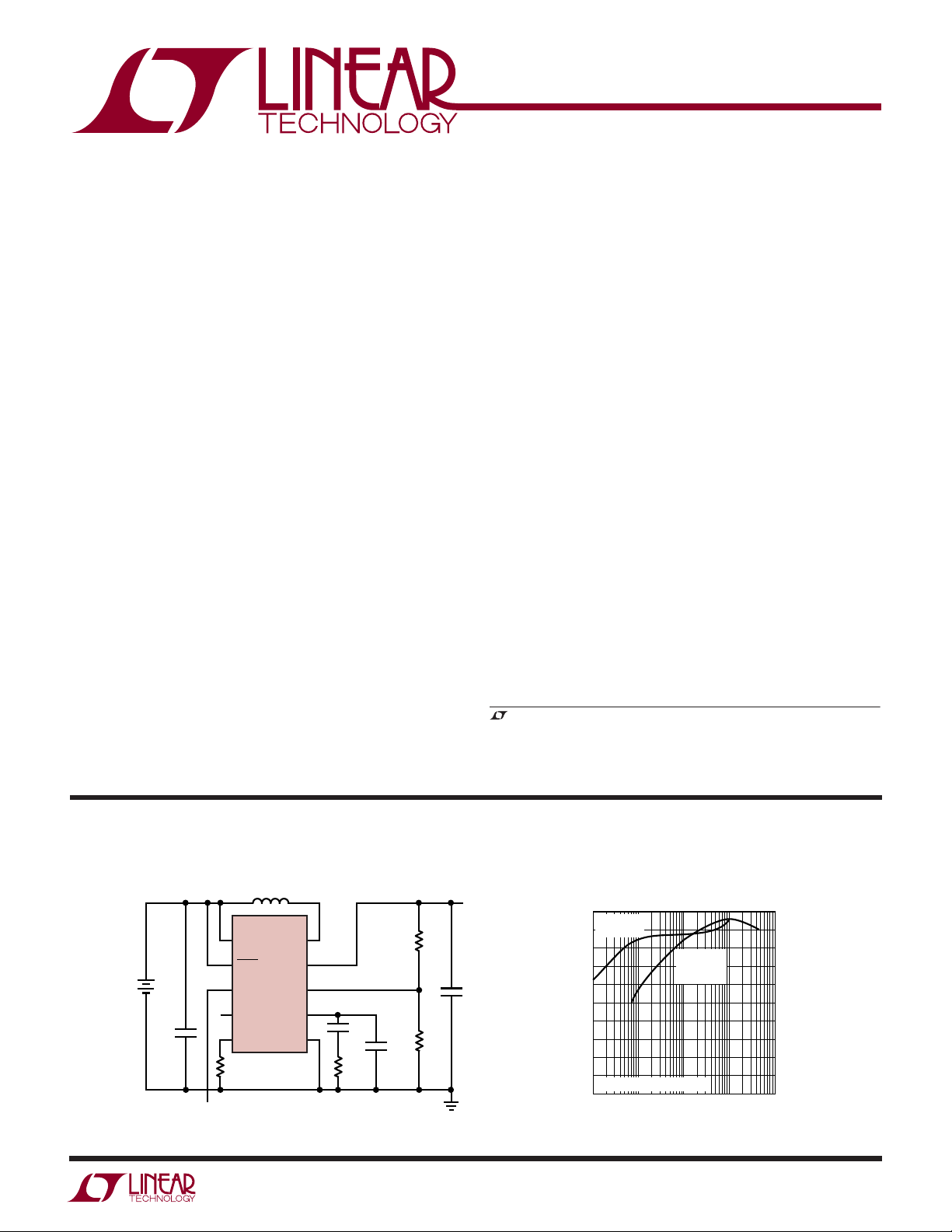
TYPICAL APPLICATION
All-Ceramic-Capacitor 2-Cell to 3.3V at 500mA Step-Up Converter
VIN = 1.8V to 3V
+
2
CELLS
C1
4.7μF
0 = FIXED FREQUENCY
1 = Burst Mode OPERATION
3
V
10
SHDN
2
MODE/SYNC
6
PGOOD
1
R
R
t
30.1k
IN
t
L1
4.7μH
LTC3401
SW
V
OUT
FB
V
C
GND
C1: TAIYO YUDEN JMK212BJ475MG
C2: TAIYO YUDEN JMK325BJ226MM
L1: SUMIDA CD43-4R7M
U
V
OUT
3.3V
500mA
4
7
8
9
C3
470pF
5
R5
82k
909k
C4
4.7pF
R2
C2
22μF
R1
549k
3404 TA01
100
Burst Mode
90
OPERATION
80
70
60
50
40
EFFICIENCY (%)
30
20
10
VIN = 2.4V WITH SCHOTTKY
0
0.1
Efficiency
1MHz
FIXED
FREQUENCY
1000
110
I
OUT
3401fb
100
(mA)
3401 TA02
1
LTC3401
PACKAGE/ORDER I FOR ATIO
UU
W
WWWU
ABSOLUTE AXI U RATI GS
(Note 1)
VIN, V
SW Voltage ................................................. – 0.5V to 6V
, Rt Voltages ......................... – 0.5V to (V
V
C
PGOOD, SHDN, FB, MODE Voltages ........... –0.5V to 6V
Operating Temperature Range (Note 2) .. –40°C to 85°C
Storage Temperature Range ................. –65°C to 125°C
Lead Temperature (Soldering, 10 sec).................. 300°C
Order Options Tape and Reel: Add #TR
Lead Free: Add #PBF Lead Free Tape and Reel: Add #TRPBF
Lead Free Part Marking: http://www.linear.com/leadfree/
Voltages ...................................... – 0.5V to 6V
OUT
OUT
+ 0.3V)
ORDER PART
TOP VIEW
10
1
R
t
MODE
2
V
3
IN
SW
4
GND
5
MS PACKAGE
10-LEAD PLASTIC MSOP
T
= 125°C
JMAX
= 130°C/ W 1 LAYER BOARD
θ
JA
= 100°C/ W 4 LAYER BOARD
θ
JA
Consult LTC Marketing for parts specified with wider operating temperature ranges.
9
8
7
6
SHDN
V
C
FB
V
OUT
PGOOD
NUMBER
LTC3401EMS
MS PART MARKING
LTPG
ELECTRICAL CHARACTERISTICS
The ● denotes specifications that apply over the full operating temperature range, otherwise specifications are at TA = 25°C.
VIN = 1.2V, V
PARAMETER CONDITIONS MIN TYP MAX UNITS
Minimum Start-Up Voltage I
Minimum Operating Voltage (Note 4) ● 0.5 V
Output Voltage Adjust Range ● 2.6 5.5 V
Feedback Voltage ● 1.22 1.25 1.28 V
Feedback Input Current VFB = 1.25V 1 50 nA
Quiescent Current—Burst Mode Operation VC = 0V, MODE/SYNC = 3.3V (Note 3) 38 65 μA
Quiescent Current—SHDN SHDN = 0V, Not Including Switch Leakage 0.1 1 μA
Quiescent Current—Active VC = 0V, MODE/SYNC = 0V, Rt = 300k (Note 3) 440 800 μA
NMOS Switch Leakage 0.1 5 μA
PMOS Switch Leakage 0.1 10 μA
NMOS Switch On Resistance 0.16 Ω
PMOS Switch On Resistance 0.18 Ω
NMOS Current Limit ● 1 1.6 A
NMOS Burst Current Limit 0.66 A
Maximum Duty Cycle Rt = 15k ● 80 85 %
Minimum Duty Cycle ● 0%
Frequency Accuracy Rt = 15k ● 1.6 2 2.4 MHz
MODE/SYNC Input High 1.4 V
MODE/SYNC Input Low 0.4 V
MODE/SYNC Input Current V
Error Amp Transconductance ΔI = – 5μA to 5μA, VC = V
PGOOD Threshold Referenced to Feedback Voltage – 6 –9 – 12 %
= 3.3V unless otherwise noted.
OUT
< 1mA 0.85 1.0 V
LOAD
MODE/SYNC
= 5.5V 0.01 1 μA
FB
85 μmhos
2
3401fb
LTC3401
ELECTRICAL CHARACTERISTICS
The ● denotes specifications that apply over the full operating temperature range, otherwise specifications are at TA = 25°C.
V
= 1.2V, V
IN
PARAMETER CONDITIONS MIN TYP MAX UNITS
PGOOD Low Voltage I
PGOOD Leakage V
SHDN Input High V
SHDN Input Low 0.4 V
SHDN Input Current V
Thermal Shutdown 170 °C
= 3.3V unless otherwise noted.
OUT
= 1mA 0.1 0.2 V
PGOOD
= 1V, I
V
OUT
= 5.5V 0.01 1 μA
PGOOD
= VIN = V
SHDN
= 5.5V 0.01 1 μA
SHDN
= 20μA 0.1 0.4 V
PGOOD
OUT
1V
Note 1: Stresses beyond those listed under Absolute Maximum Ratings
may cause permanent damage to the device. Exposure to any Absolute
Maximum Rating condition for extended periods may affect device
reliability and lifetime.
Note 2: The LTC3401 is guaranteed to meet performance specifications
from 0°C to 70°C. Specifications over the –40°C to 85°C operating
temperature range are assured by design, characterization and correlation
with statistical process controls.
Note 3: Current is measured into V
bootstrapped to the V
supply by (V
Note 4: Once the output is started, the IC is not dependant upon the V
supply.
UW
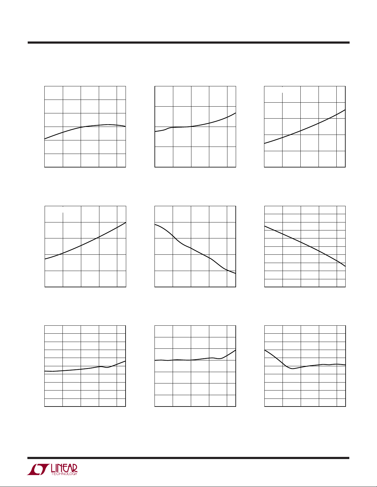
TYPICAL PERFOR A CE CHARACTERISTICS
SW Pin and Inductor Current (IC)
in Discontinuous Mode. Ringing
Control Circuitry Eliminates High
Switching Waveform on SW Pin
50mA/DIV
SW
1V/DIV
Frequency Ringing Transient Response 5mA to 50mA
I
L
0A
SW
1V/DIV
0V
since the supply current is
V
OUT
50mA
5mA
OUT
pin and in the application will reflect to the input
OUT
) • I/ Efficiency. The outputs are not switching.
OUT/VIN
100mV/DIV
I
OUT
IN
50ns/DIV
3401 G01
200ns/DIV
3401 G02
C
= 22μF 200μs/DIV 3401 G03
OUT
L = 3.3μH
= 1MHz
f
OSC
3401fb
3
LTC3401
UW
TYPICAL PERFOR A CE CHARACTERISTICS
Transient Response 50mA to 500mA
V
OUT
200mV/DIV
550mA
I
OUT
50mA
C
= 22μF 200μs/DIV 3401 G04
OUT
L = 3.3μH
= 1MHz
f
OSC
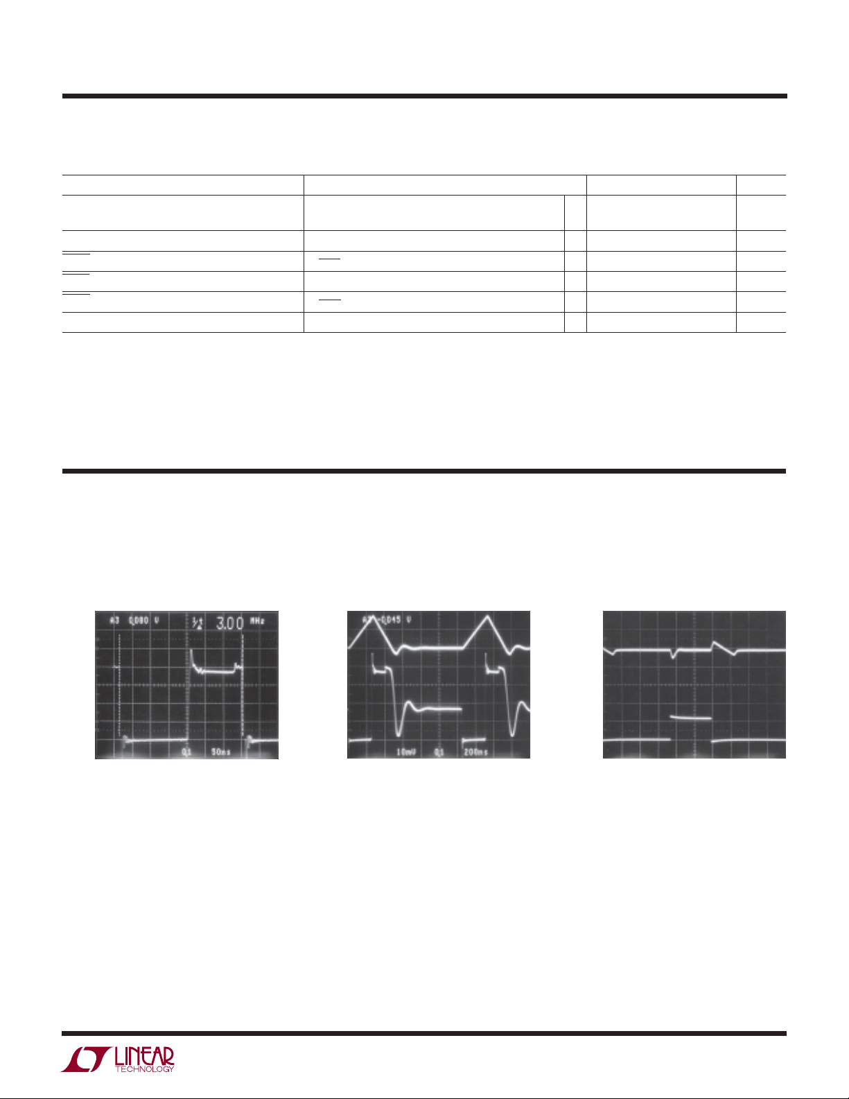
Converter Efficiency 1.2V to 3.3V
100
90
Burst Mode
80
OPERATION
70
60
50
40
EFFICIENCY (%)
30
20
10
0
0.1 10 100 1000
300kHz
1MHz
1
OUTPUT CURRENT (mA)
3MHz
3401 G07
Burst Mode Operation
V
OUT
AC
100mV/DIV
SW
1V/DIV
VIN = 1.2V 5ms/DIV 3401 G05
V
= 3.3V
OUT
= 100μF
C
OUT
= 250μA
I
OUT
MODE/SYNC PIN = HIGH
Converter Efficiency 2.4V to 3.3V
100
Burst Mode
90
OPERATION
80
70
300kHz
60
50
40
EFFICIENCY (%)
30
20
10
0
0.1 10 100 1000
1
OUTPUT CURRENT (mA)
3MHz
1MHz
3401 G08
Burst Mode Operation
V
OUT
AC
100mV/DIV
SW
1V/DIV
VIN = 1.2V 200μs/DIV 3401 G06
V
= 3.3V
OUT
= 100μF
C
OUT
= 20mA
I
OUT
MODE/SYNC PIN = HIGH
Converter Efficiency 3.6V to 5V
100
Burst Mode OPERATION
90
80
70
60
50
40
EFFICIENCY (%)
30
20
10
0
0.1
1MHz
FIXED
FREQUENCY
110
LOAD CURRENT (mA)
100
1000
3401 G10
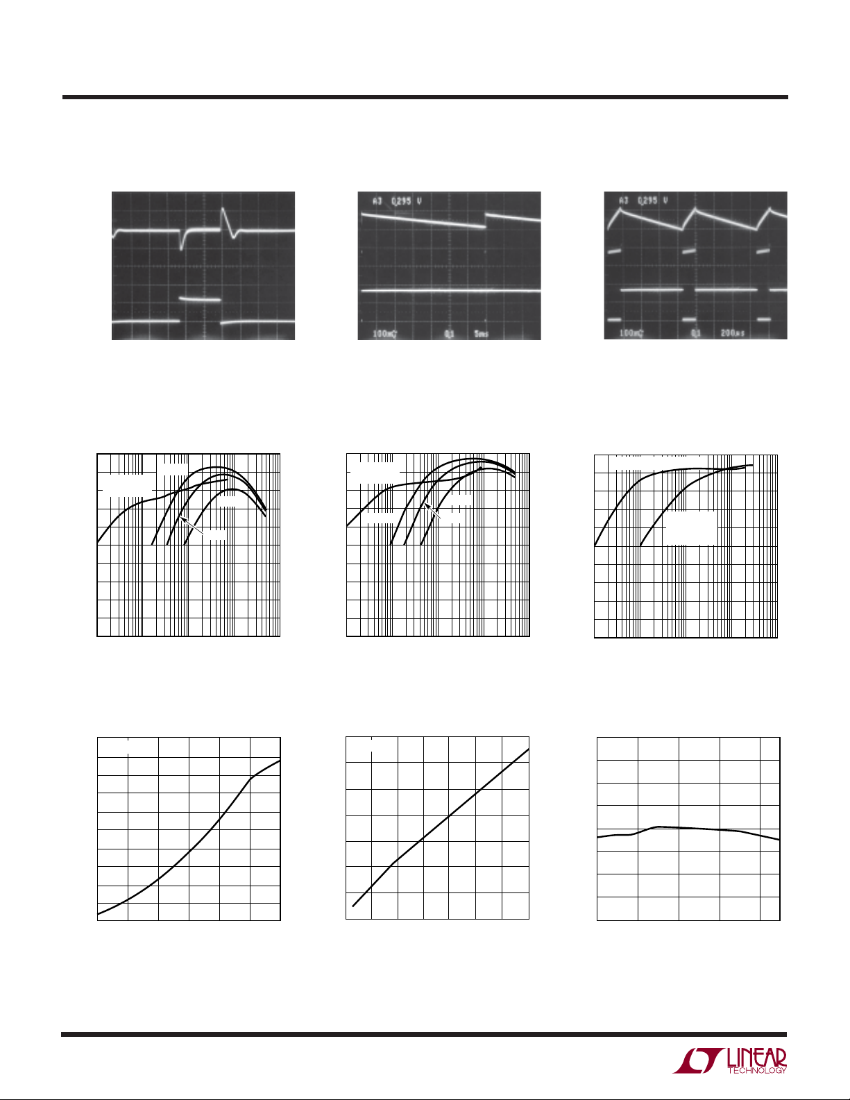
Start-Up Voltage
vs I
OUT
500
TA = 25°C
400
300
200
OUTPUT CURRENT (mA)
100
0
0.8
0.9
4
1
1.1 1.2
VIN (V)
1.3
3401 G09
1.4
Efficiency Loss Without Schottky
vs Frequency
14
= 25°C
T
A
12
10
8
6
4
EFFICIENCY LOSS (%)
2
0
0.2
0.6 1.0
FREQUENCY (MHz)
1.8 2.6 3.0
1.4 2.2
3401 G11
Current Limit
1.80
1.75
1.70
1.65
1.60
1.55
CURRENT (A)
1.50
1.45
1.40
–15 25 105
–55
TEMPERATURE (°C)
3401fb
65
125
3401 G12
UW
TYPICAL PERFOR A CE CHARACTERISTICS
LTC3401
EA FB Voltage
1.28
1.27
1.26
1.25
VOLTAGE (V)
1.24
1.23
1.22
–55
PMOS R
0.30
V
OUT
0.25
0.20
0.15
RESISTANCE (Ω)
0.10
0.05
–55
–15 25 105
TEMPERATURE (°C)
65
DS(ON)
= 3.3V
–15 25 105
TEMPERATURE (°C)
65
3401 G13
3401 G16
125
125
Oscillator Frequency Accuracy
2.10
Rt = 15k
2.05
2.00
FREQUENCY (MHz)
1.95
1.90
–15 25 105
–55
TEMPERATURE (°C)
Start-Up Voltage
1.1
1.0
0.9
0.8
VOLTAGE (V)
0.7
0.6
–15 25 105
–55
TEMPERATURE (°C)
NMOS R
0.30
0.25
0.20
0.15
RESISTANCE (Ω)
0.10
65
125
3401 G14
0.05
–55
DS(ON)
V
= 3.3V
OUT
–15 25 105
TEMPERATURE (°C)
65
125
3401 G22
Shutdown Threshold
1.10
1.05
1.00
0.95
0.90
0.85
0.80
VOLTAGE (V)
0.75
0.70
0.65
65
125
3401 G17
0.60
–15 25 105
–55
TEMPERATURE (°C)
65
125
3401 G18
PGOOD Threshold
–7.0
–7.5
–8.0
–8.5
(%)
FB
–9.0
–9.5
–10.0
–10.5
PERCENT FROM V
–11.0
–11.5
–12.0
–55
–15 25 105
TEMPERATURE (°C)
65
3401 G19
125
Burst Mode Operation Current
44
42
40
38
36
CURRENT (μA)
34
32
30
–15 25 105
–55
TEMPERATURE (°C)
V
Turn-Off Voltage
OUT
2.50
2.45
2.40
2.35
2.30
2.25
2.20
VOLTAGE (V)
2.15
2.10
2.05
65
125
3401 G20
2.00
–15 25 105
–55
TEMPERATURE (°C)
3401fb
65
125
3401 G21
5

LTC3401
U
UU
PI FU CTIO S
Rt (Pin 1): Timing Resistor to Program the Oscillator
Frequency.
10
•
OSC
310
=
Hz
R
t
f
MODE/SYNC (Pin 2): Burst Mode Select and Oscillator
Synchronization.
MODE/SYNC = High. Enable Burst Mode operation. The
inductor peak inductor current will be 1/3 the current
limit value and return to zero current on each cycle.
During Burst Mode operation the operation is variable
frequency, providing a significant efficiency improvement at light loads. It is recommended the Burst Mode
operation only be entered once the part has started up.
MODE/SYNC = Low. Disable Burst Mode operation and
maintain low noise, constant frequency operation.
MODE/SYNC = External CLK. Synchronization of the
internal oscillator and Burst Mode operation disable. A
clock pulse width of 100ns to 2μs is required to
synchronize.
VIN (Pin 3): Input Supply Pin.
SW (Pin 4): Switch Pin. Connect inductor and Schottky
diode here. For applications with output voltages over
4.3V, a Schottky diode is required to ensure that the SW
pin voltage does not exceed its absolute maximum rating.
Minimize trace length to keep EMI down. For discontinuous inductor current, a controlled impedance is placed
from SW to VIN from the IC to eliminate high frequency
ringing due to the resonant tank of the inductor and SW
node capacitance, therefore reducing EMI radiation.
GND (Pin 5): Signal and Power Ground for the IC.
PGOOD (Pin 6): Power Good Comparator Output. This
open-drain output is low when V
regulation voltage.
V
(Pin 7): Output of the Synchronous Rectifier and
OUT
Bootstrapped Power Source for the IC. A ceramic capacitor of at least 1μF is required and should be located as
close to the V
FB (Pin 8): Feedback Pin. Connect resistor divider tap
here. The output voltage can be adjusted from 2.6V to
5.5V. The feedback reference voltage is typically 1.25V.
VC (Pin 9): Error Amp Output. A frequency compensation
network is connected to this pin to compensate the loop.
See the section “Compensating the Feedback Loop” for
guidelines.
SHDN (Pin 10): Shutdown. Grounding this pin shuts down
the IC. Tie to >1V to enable (VIN or digital gate output). To
operate with input voltages below 1V once the converter
has started, a 1M resistor from SHDN to VIN, and a 5M
resistor from SHDN to V
esis During shutdown the output voltage will hold up to V
minus a diode drop due to the body diode of the PMOS
synchronous switch. If the application requires a complete disconnect during shutdown then refer to section
“Output Disconnect Circuits”.
and GND pins as possible (Pins 7 and 5).
OUT
will provide sufficient hyster-
OUT
< –9% from its
FB
IN
6
3401fb
 Loading...