

Page 1
Description
DEMO MANUAL DC2326A
LTC2345
16-/18-Bit, Octal 200ksps, SAR ADC
Demonstration circuit 2326A shows the proper way to drive
®
the LTC
2345 ADC. The LTC2345 is a low noise, high speed,
simultaneous sampling 16-/18-bit successive approximation
register (SAR) ADC. The LTC2345 has a flexible SoftSpan
interface that allows conversion-by-conversion control of
the input voltage span on a per-channel basis. An internal
2.048V reference and 2× buffer simplify basic operation
while an external reference can be used to increase the
input range and the SNR of the ADC.
The DC2326A demonstrates the DC and AC performance of
the LTC2345 in conjunction with the DC590/DC2026 and
DC890 data collection boards. Use the DC590/DC2026 to
demonstrate DC performance such as peak-to-peak noise
and DC linearity. Use the DC890 if precise sampling rates
are required or to demonstrate AC performance such as
™
SNR, THD, SINAD and SFDR. The DC2326A is intended
to demonstrate recommended grounding, component
placement and selection, routing and bypassing for this
ADC. A suggested driver circuit for the analog inputs is
also presented.
Design files for this circuit board including the schematic,
layout and BOM are available at
http://www.linear.com/demo/DC2326A
L, LT, LTC, LTM, Linear Technology and the Linear logo are registered trademarks and PScope,
QuikEval and SoftSpan are trademarks of Linear Technology Corporation. All other trademarks
are the property of their respective owners.
assembly options
Assembly
Version U1 Part Number
DC2326A-A
DC2326A-B LTC2345-16 200ksps 8 16 60MHz 300
LTC2345-18 200ksps 8 18 60MHz 300
Max Conversion
Rate
Number of
Channels
Number of
Bits
Max CLK IN
Frequency
CLK IN/fs
Ratio
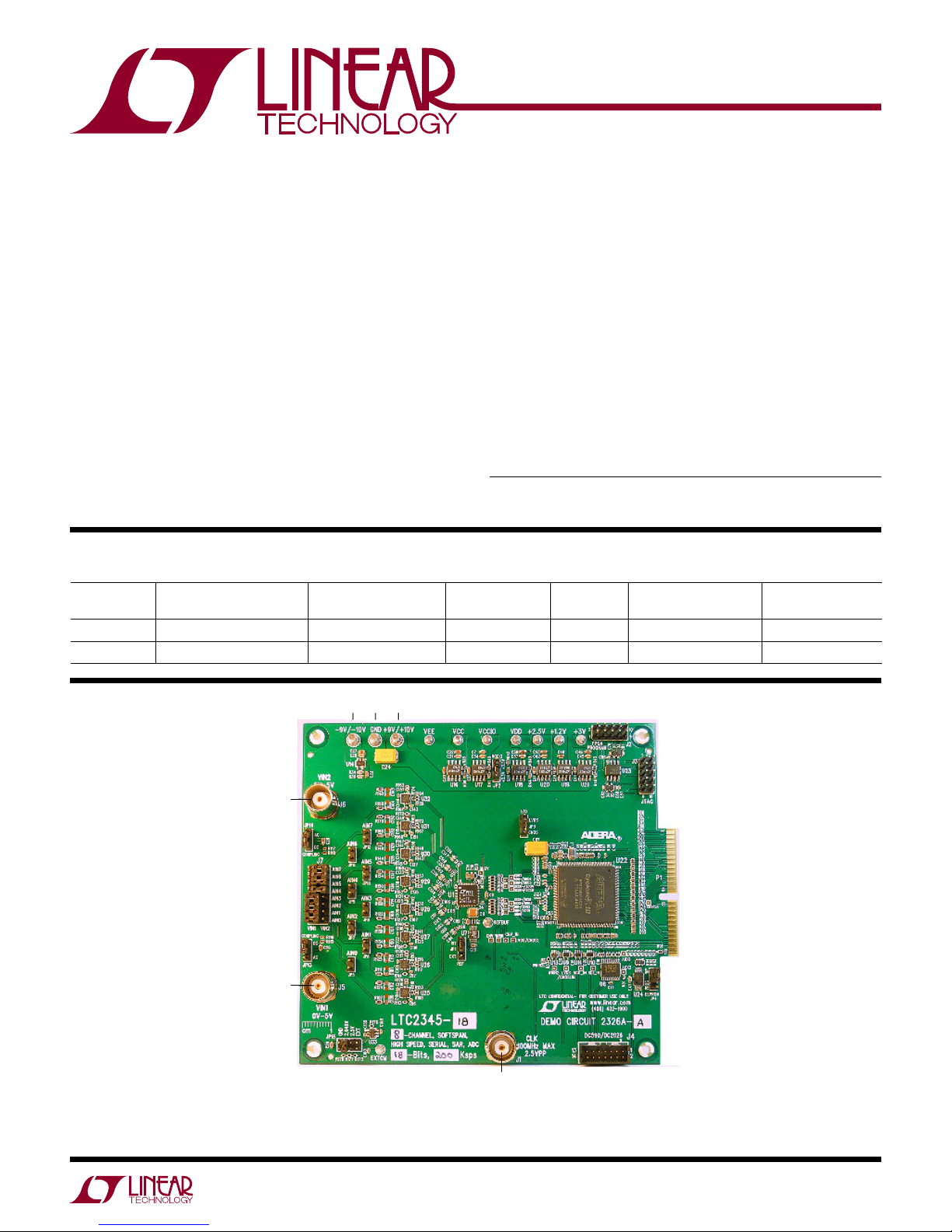
boarD photo
0V to 4.096V
0V to 4.096V
+9V
GND
–9V
V
IN2
DC890
V
IN1
CLK
100MHz MAX
2.5V
P-P
Figure 1. DC2326A Connection Diagram
DC590 OR DC2026
dc2326af
1
Page 2

DEMO MANUAL DC2326A
Dc890 Quick start proceDure
Check to make sure that all jumpers are set to their default
settings as described in the DC2326A Jumpers section of
this manual. The default connections configure the ADC to
use the onboard reference and regulators to generate all
the required bias voltages. The analog inputs by default are
DC coupled. Connect the DC2326A to a DC890 USB High
Speed Data Collection Board using connector P1. Then,
connect the DC890 to a host PC with a standard USB A/B
cable. Apply ±9V to the indicated terminals. Then apply
a low jitter signal source to J5 and J6. Use J7 to route
the signal sources of J5 and J6 to the desired AIN0-AIN7
inputs. Observe the recommended input voltage range
for each analog input. Connect a low jitter 2.5V
wave or square wave to connector J1. See the Assembly
Options table for the appropriate clock frequency. Note
that J1 has a 50Ω termination resistor to ground.
P-P
sine
™
Run the PScope
later) which can be downloaded from www.linear.com/
designtools/software.
Complete software documentation is available from the
Help menu. Updates can be downloaded from the
menu.
may be added.
The PScope software should recognize the DC2326A and
configure itself automatically.
Click the Collect button (See Figure 3) to begin acquiring
data. The Collect button then changes to Pause, which
can be clicked to stop data acquisition.
Check for updates periodically as new features
software (Pscope.exe version K82 or
Tools
Dc590/Dc2026 Quick start proceDure
IMPORTANT! To avoid damage to the DC2326A, make
sure that VCCIO (JP6 of the DC590, JP3 of the DC2026)
of the DC590/DC2026 is set to 3.3V before connecting
the DC590/DC2026 to the DC2326A.
To use the DC590/DC2026 with the DC2326A, it is necessary
to apply ±9V and ground to the ±9V and GND terminals of
the DC2326A. Connect the DC590/DC2026 to a host PC
with a standard USB A/B cable. Connect the DC2326A to
a DC590/DC2026 USB serial controller using the supplied
14-conductor ribbon cable. Apply a signal source to J5
and J6. Use J7 to route the signal sources of J5 and J6
to the desired AIN0-AIN7 inputs. No Clock is required on
J1 when using the DC590/DC2026. The clock signal is
provided by the DC590/DC2026.
Run the QuikEval software (quikeval.exe version K103 or
later) which is available from www.linear.com/designtools/
software. The correct control panel will be loaded auto
matically. Click
reading the ADC.
-
the COLLECT button (Figure 6) to begin
2
dc2326af
Page 3
Dc2326a setup
IN0
R107
0Ω
C100
OPT
U25B
LT6237IDD
R113
0Ω
DEMO MANUAL DC2326A
C96
V
CC
0.1µF
R108
+
C104
–
0.1µF
V
EE
49.9Ω
C94
1000pF
C98
OPT
IN0
+
R124
0Ω
V
CM
C112
OPT
R119
1k
+
–
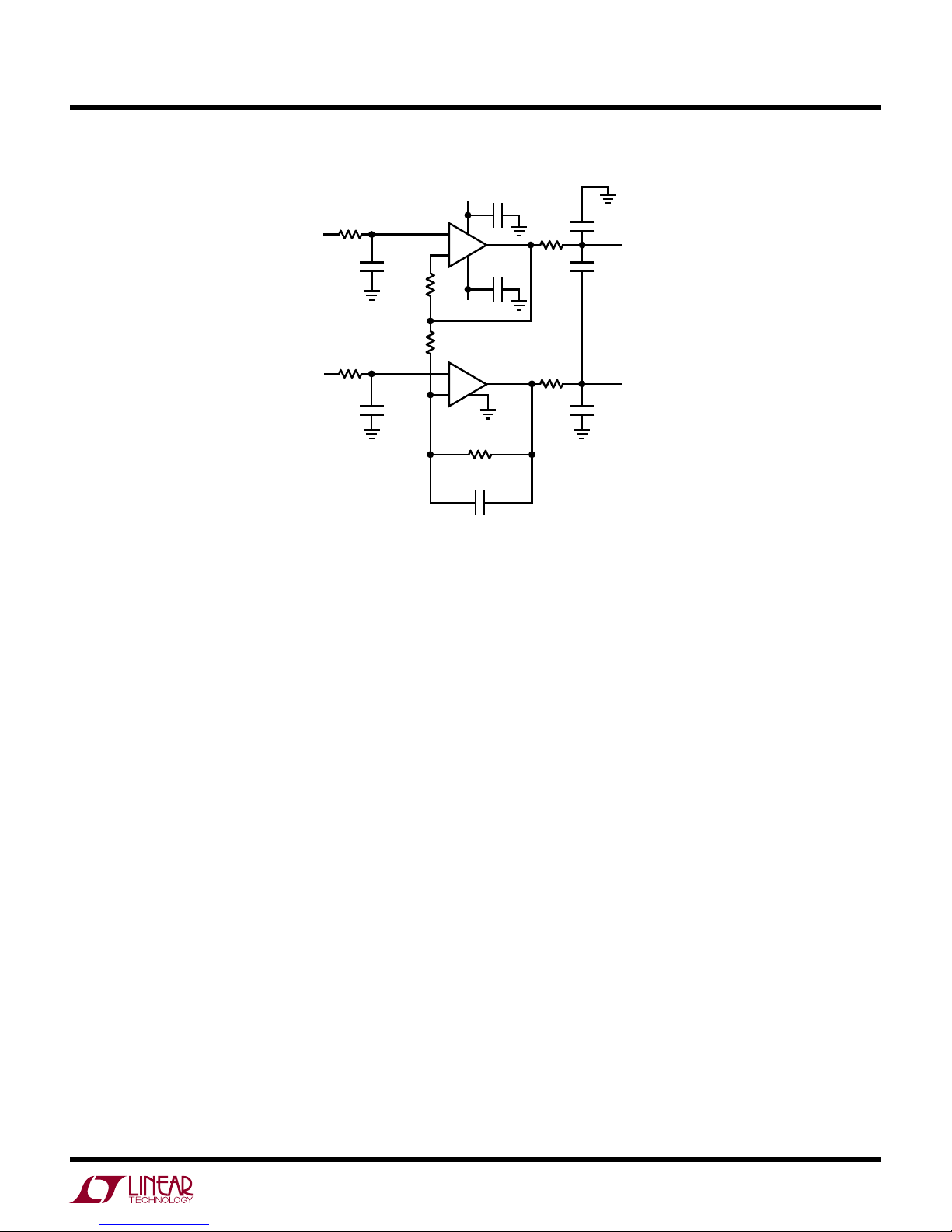
Figure 2. 0V–4.096V Single-Ended to Fully Differential DC Coupled Driver
DC Power
The DC2326A requires ±9VDC and draws +145mA/–65mA.
Most of the supply current is consumed by the FPGA,
opamps, regulators and discrete logic on the board. The
±9VDC input voltage powers the ADC through LT1763
regulators which provide protection against accidental
reverse bias. Additional regulators provide power for the
FPGA and opamps.
U25A
LT6237IDD
EN
R129
1k
C116
OPT
dc2326 F02
R123
49.9Ω
C102
1000pF
IN0
–
conversion rate is shown in the Assembly Options table. If
the clock input is to be driven with logic, it is recommended
that the 49.9Ω termination resistor (R4) be removed.
Driving R4 with discrete logic may result in slow rising
edges. These slow rising edges may compromise the SNR
the converter
of
in the presence of high-amplitude higher
frequency input signals.
Data Output
Clock Source
You must provide a low jitter 2.5V
P-P
to the clock input, J1. The clock input is AC coupled so the
DC level of the clock signal is not important. A generator
such as the Rohde & Schwarz SMB100A high speed clock
source is recommended to drive the clock input. Even a
good generator can start to produce noticeable jitter at
low frequencies. Therefore it is recommended for lower
sample rates to divide down a higher frequency clock to
the desired sample rate. The ratio of clock frequency to
sine or square wave
Parallel data output from this board (0V to 2.5V default),
if not connected to the DC890, can be acquired by a logic
analyzer, and subsequently imported into a spreadsheet, or
mathematical package depending on what form of digital
signal processing is desired. Alternatively, the data can
be fed directly into an application circuit. Use pin 50 of
P1 to latch the data. The data should be latched using the
negative edge of this signal. The data output signal levels
at P1 can also be increased to 0V-3.3V if the application
circuit requires a higher voltage. This is accomplished by
moving JP2 to the 3.3V position.
dc2326af
3
Page 4

DEMO MANUAL DC2326A
Dc2326a setup
Reference
The default reference is the LTC2345 internal 4.096V
reference. Alternatively, if a higher reference voltage is
desired, the LTC6655-5 reference (U7) can be used by
setting the REF jumper (JP1) to the EXT position and
installing a 0Ω resistor in the R7 position. This should
result in better SNR performance but may slightly degrade
the THD performance of the LTC2345.
Analog Inputs
All eight inputs have the same driver circuitry. The circuit of
Figure 2 shows the driver for IN0. It provides a DC coupled
single-ended to fully differential output to the analog inputs
of the LTC2345 with a maximum 0V-4.096V input signal.
DC890 Data Collection
For SINAD, THD or SNR testing a low noise, low distortion
generator such as the B&K Type 1051 or Stanford Research
SR1 should be used. A low jitter RF oscillator such as the
Rohde & Schwarz SMB100A is used to drive the clock
input. This demo board is tested in house by attempting
to duplicate the FFT plot shown in Typical Performance
Characteristics section of the LTC2345 data sheet. This
involves using a 60MHz clock source, along with a sinu
soidal generator at a frequency of approximately 2kH
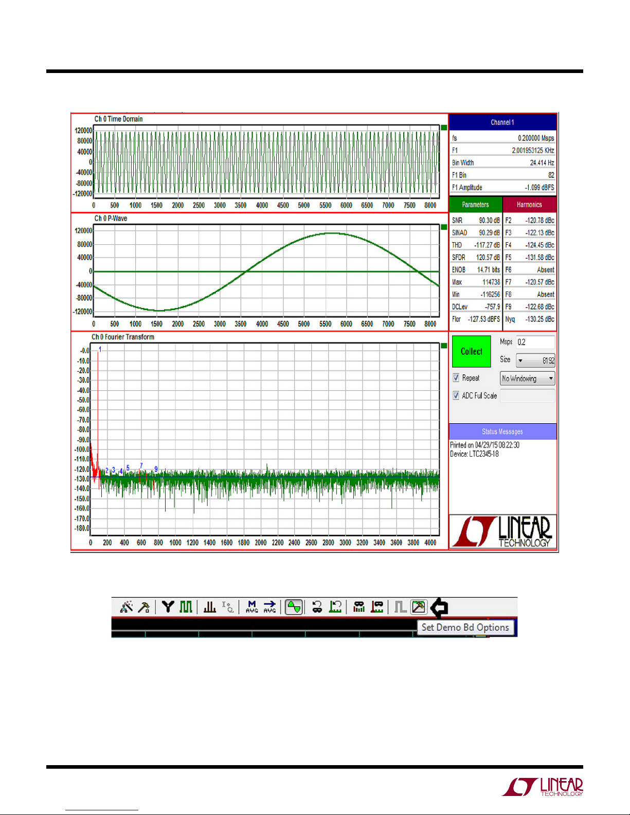
input signal level is approximately –1dBFS. A typical F
obtained with DC2326A is shown in Figure 3. Note that
to calculate the real SNR, the signal level (F1 amplitude =
–1.099dB) has to be added back to the SNR that PScope
displays. With the example shown in Figure 3 this means
that the actual SNR would be 91.40dB instead of the
90.30dB that PScope displays. Taking the RMS sum of the
recalculated SNR and the THD yields a SINAD of 91.39dB
which is fairly close to the typical number for this ADC.
-
z. The
FT
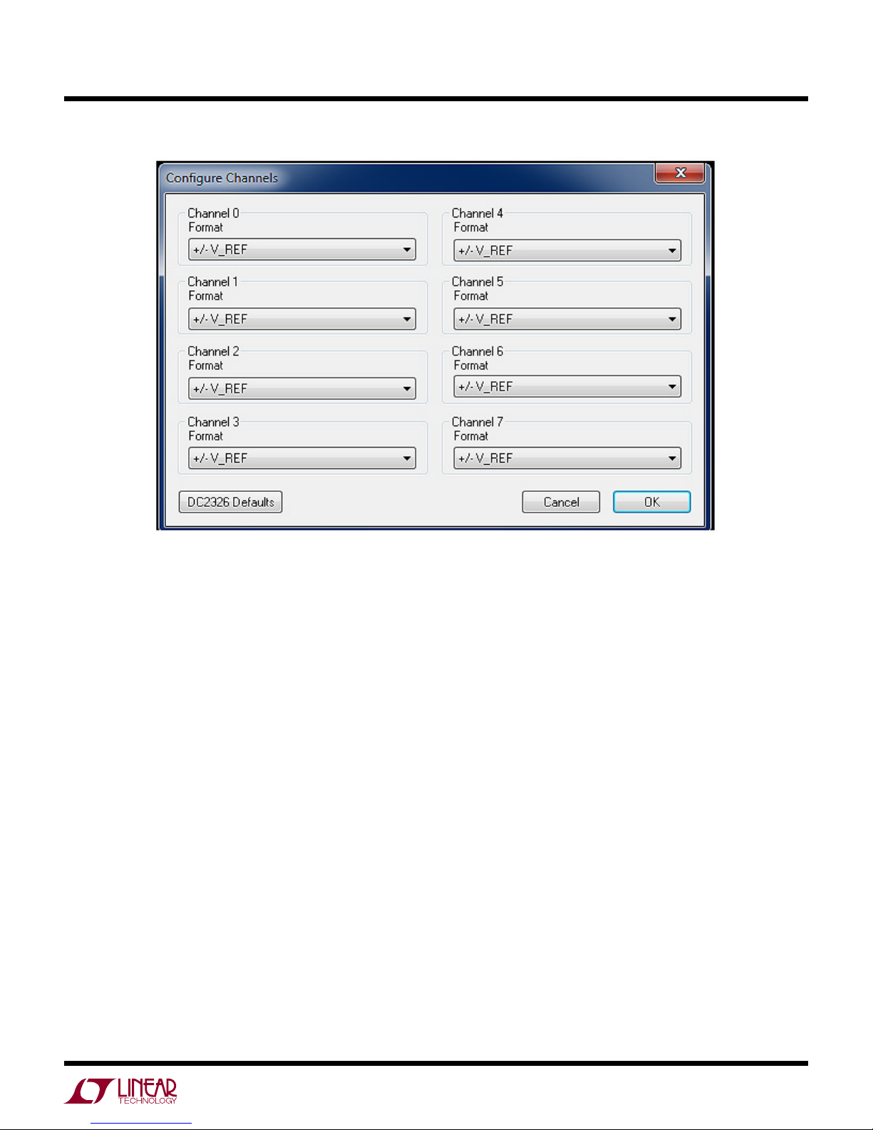
To change the default settings for the LTC2345 in PScope,
click on the Set Demo Bd Options button in the PScope
tool bar shown in Figure 4. This will open the Configure
Channels menu of Figure 5. In this menu it is possible to
set the input signal range setting for each channel. There
is also a button to return PScope to the default DC2326A
settings which are optimized for the default hardware
settings of the DC2326A.
There are a number of scenarios that can produce mislead
ing results when evaluating an ADC. One that is common
is feeding the converter with an input frequency that is
-multiple of the sample rate, and which will only
a sub
exer
cise a small subset of the possible output codes.
The proper method is to pick an M/N frequency for the
input sine wave frequency. N is the number of samples
in the FFT. M is a prime number between one and N/2.
Multiply M/N by the sample rate to obtain the input sine
wave frequency. Another scenario that can yield poor
results is if you do not have a signal generator capable of
ppm frequency accuracy or if it cannot be locked to the
clock frequency. You can use an FFT with windowing to
reduce the “leakage” or spreading of the fundamental, to
get a close approximation of the ADC performance. If an
amplifier or clock source with poor phase noise is used,
the windowing will not improve the SNR.
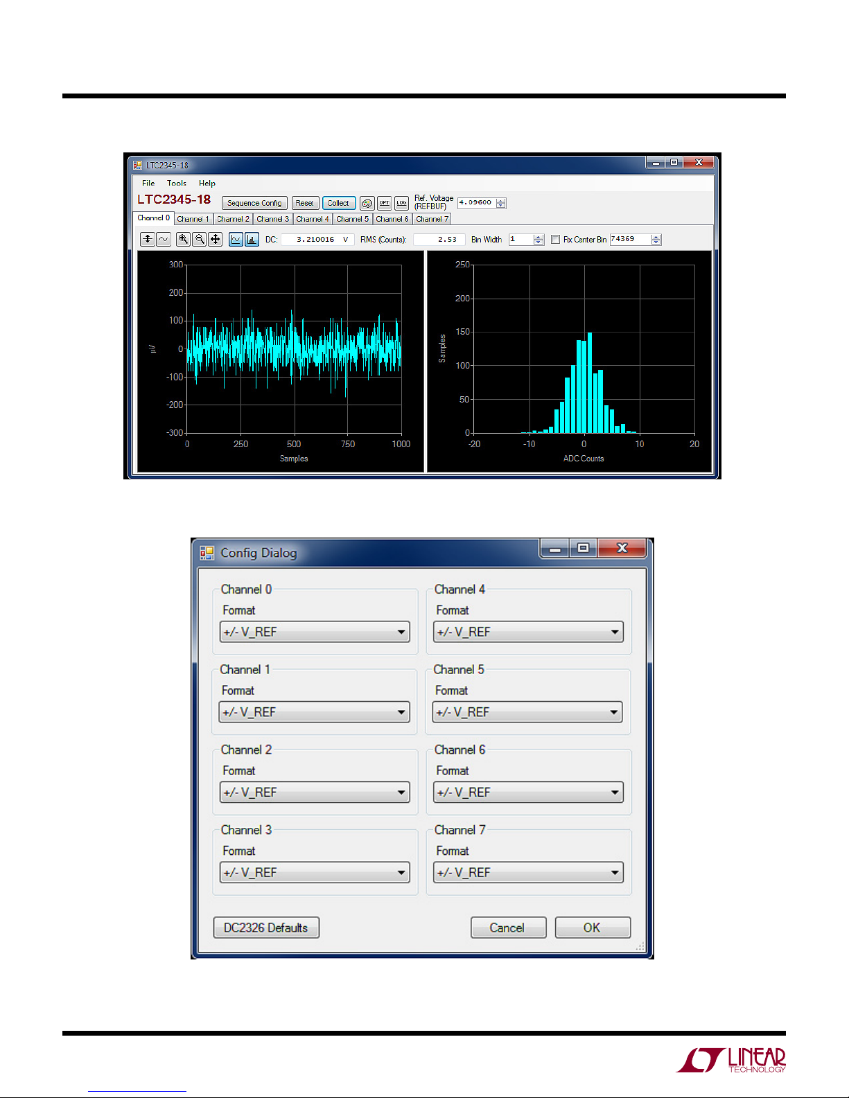
DC590/DC2026 Data Collection
Due to the relatively low and somewhat unpredictable
sample rate of the DC590/DC2026 its usefulness is lim
noise measurement and data collection of slowly
ited to
moving
shown in Figure 6. To change the default settings for the
LTC2345 in QuikEval, click on the Sequence
ton. This will open the Config Dialog menu of Figure 7.
In
and
is also a button to return QuikEval to the default DC2326A
settings which are optimized for the default hardware set
tings of the DC2326A.
signals. A typical data capture and histogram are
Config but-
this menu it is possible to set the input signal range
gain compression setting for each sequence. There
-
-
-
4
dc2326af
Page 5

Dc2326a setup
DEMO MANUAL DC2326A
Layout
As with any high performance ADC, this part is sensitive
to layout. The area immediately surrounding the ADC on
the DC2326A should be used as a guideline for placement,
and routing of the various components associated with
the ADC. Here are some things to remember when laying
out a board for the LTC2345. A ground plane is necessary
to obtain maximum performance. Keep bypass capacitors
as close to supply pins as possible. Use individual low
impedance returns for all bypass capacitors. Use of a
symmetrical layout around the analog inputs will minimize
the effects of parasitic elements. Shield analog input traces
with ground to minimize coupling from other traces. Keep
traces as short as possible.
Component Selection
When driving a low noise, low distortion ADC such as the
LTC2345, component selection is important so as to not
degrade performance. Resistors should have low values
to minimize noise and distortion. Metal film resistors are
recommended to reduce distortion caused by self heat
ing. Because of their low voltage coefficients, to further
reduce distortion NPO or silver mica capacitors should be
used. Any buffer used to drive the LTC2345 should have
low distortion, low noise and a
the LT1355.
fast settling time such as
-
dc2326af
5
Page 6
DEMO MANUAL DC2326A
Dc2326a setup
6
Figure 3. PScope Screen Shot
Figure 4. PScope Tool Bar
dc2326af
Page 7
Dc2326a setup
DEMO MANUAL DC2326A
Figure 5. PScope Configuration Menu
dc2326af
7
Page 8
DEMO MANUAL DC2326A
Dc2326a setup
Figure 6. QuikEval Screen Shot
8
Figure 7. QuikEval Configuration Menu
dc2326af
Page 9

Dc2326a jumpers
DEMO MANUAL DC2326A
Definitions
JP1: REF selects INT or EXT reference for the ADC. The
default setting is INT.
JP2: VCCIO sets the output levels at P1 to either 3.3V
or 2.5V. Use 2.5V to interface to the DC890 which is the
default setting. Use 3.3V to interface to the DC2026.
JP3: I/O selects LVDS or CMOS logic levels. The default
setting is CMOS. Only CMOS is currently supported.
Dc2326a connectors
Definitions
P1: DC890 interface is used to communicate with the
DC890 controller.
J1: CLK provides the master clock for the DC2326A when
interfaced to the DC890.
J2: FPGA PROGRAM is used to program the FPGA. This
is for factory use only.
JP4: EEPROM is for factory use only. The default posi
tion is WP.
JP5-JP12:
inputs to ground or can be used drive the individual AIN
inputs. The default is to leave these open.
JP13-JP14: Coupling selects AC or DC coupling for V
and V
J3: JTAG is for factory use only.
J4: DC590/DC2026 interface is used to communicate with
DC2026 Linduino controller or DC590.
the
J5
and J6: Provide analog input voltages to AIN0-AIN7
of the ADC.
J7: Routes the signals of J5 and J6 to AIN0-AIN7.
AIN0-AIN7 can be used to short individual AIN
. Default setting is DC.
IN2
IN1
-
Information furnished by Linear Technology Corporation is believed to be accurate and reliable.
However, no responsibility is assumed for its use. Linear Technology Corporation makes no representation that the interconnection of its circuits as described herein will not infringe on existing patent rights.
dc2326af
9
Page 10

DEMO MANUAL DC2326A
DEMONSTRATION BOARD IMPORTANT NOTICE
Linear Technology Corporation (LT C) provides the enclosed product(s) under the following AS IS conditions:
This demonstration board (DEMO BOARD) kit being sold or provided by Linear Technology is intended for use for ENGINEERING DEVELOPMENT
OR EVALUATION PURPOSES ONLY and is not provided by LT C for commercial use. As such, the DEMO BOARD herein may not be complete
in terms of required design-, marketing-, and/or manufacturing-related protective considerations, including but not limited to product safety
measures typically found in finished commercial goods. As a prototype, this product does not fall within the scope of the European Union
directive on electromagnetic compatibility and therefore may or may not meet the technical requirements of the directive, or other regulations.
If this evaluation kit does not meet the specifications recited in the DEMO BOARD manual the kit may be returned within 30 days from the date
of delivery for a full refund. THE FOREGOING WARRANTY IS THE EXCLUSIVE WARRANTY MADE BY THE SELLER TO BUYER AND IS IN LIEU
OF ALL OTHER WARRANTIES, EXPRESSED, IMPLIED, OR STATUTORY, INCLUDING ANY WARRANTY OF MERCHANTABILITY OR FITNESS
FOR ANY PARTICULAR PURPOSE. EXCEPT TO THE EXTENT OF THIS INDEMNITY, NEITHER PARTY SHALL BE LIABLE TO THE OTHER FOR
ANY INDIRECT, SPECIAL, INCIDENTAL, OR CONSEQUENTIAL DAMAGES.
The user assumes all responsibility and liability for proper and safe handling of the goods. Further, the user releases LT C from all claims
arising from the handling or use of the goods. Due to the open construction of the product, it is the user’s responsibility to take any and all
appropriate precautions with regard to electrostatic discharge. Also be aware that the products herein may not be regulatory compliant or
agency certified (FCC, UL, CE, etc.).
No License is granted under any patent right or other intellectual property whatsoever. LTC assumes no liability for applications assistance,
customer product design, software performance, or infringement of patents or any other intellectual property rights of any kind.
LT C currently services a variety of customers for products around the world, and therefore this transaction is not exclusive.
Please read the DEMO BOARD manual prior to handling the product. Persons handling this product must have electronics training and
observe good laboratory practice standards. Common sense is encouraged.
This notice contains important safety information about temperatures and voltages. For further safety concerns, please contact a LTC application engineer.
Mailing Address:
Linear Technology
1630 McCarthy Blvd.
Milpitas, CA 95035
Copyright © 2004, Linear Technology Corporation
Linear Technology Corporation
10
1630 McCarthy Blvd., Milpitas, CA 95035-7417
(408) 432-1900 ● FAX: (408) 434-0507 ● www.linear.com
dc2326af
LT 0815 • PRINTED IN USA
LINEAR TECHNOLOGY CORPORATION 2015
 Loading...