

Page 1
FEATURES
■
Integrated Dual 10-Bit ADCs
■
Sample Rate: 65Msps/40Msps/25Msps
■
Single 3V Supply (2.7V to 3.4V)
■
Low Power: 400mW/235mW/150mW
■
61.8dB SNR
■
85dB SFDR
■
110dB Channel Isolation at 100MHz
■
Multiplexed or Separate Data Bus
■
Flexible Input: 1V
■
575MHz Full Power Bandwidth S/H
■
Clock Duty Cycle Stabilizer
■
Shutdown and Nap Modes
■
Pin Compatible Family
P-P
to 2V
P-P
Range
105Msps: LTC2282 (12-Bit), LTC2280 (10-Bit)
80Msps: LTC2294 (12-Bit), LTC2289 (10-Bit)
65Msps: LTC2293 (12-Bit), LTC2288 (10-Bit)
40Msps: LTC2292 (12-Bit), LTC2287 (10-Bit)
25Msps: LTC2291 (12-Bit), LTC2286 (10-Bit)
10Msps: LTC2290 (12-Bit), LTC2292 (14-Bit)
■
64-Pin (9mm × 9mm) QFN Package
U
APPLICATIO S
■
Wireless and Wired Broadband Communication
■
Imaging Systems
■
Spectral Analysis
■
Portable Instrumentation
LTC2288/LTC2287/LTC2286
Dual 10-Bit, 65/40/25Msps
Low Noise 3V ADCs
U
DESCRIPTIO
The LTC®2288/LTC2287/LTC2286 are 10-bit 65Msps/
40Msps/25Msps, low noise dual 3V A/D converters designed for digitizing high frequency, wide dynamic range
signals. The LTC2288/LTC2287/LTC2286 are perfect for
demanding imaging and communications applications
with AC performance that includes 61.8dB SNR and 85dB
SFDR for signals at the Nyquist frequency.
DC specs include ±0.1LSB INL (typ), ±0.05LSB DNL (typ)
and ±0.6 LSB INL, ±0.5 LSB DNL over temperature. The
transition noise is a low 0.07LSB
A single 3V supply allows low power operation. A separate
output supply allows the outputs to drive 0.5V to 3.6V
logic. An optional multiplexer allows both channels to
share one digital output bus.
A single-ended CLK input controls converter operation. An
optional clock duty cycle stabilizer allows high performance at full speed for a wide range of clock duty cycles.
, LTC and LT are registered trademarks of Linear Technology Corporation.
All other trademarks are the property of their respective owners.
RMS
.
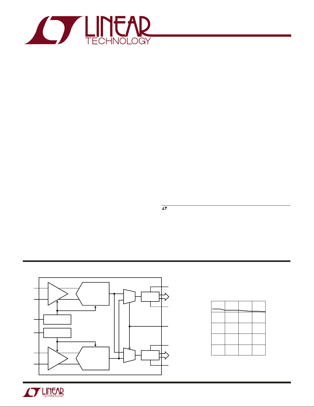
TYPICAL APPLICATIO
ANALOG
INPUT A
CLK A
CLK B
ANALOG
INPUT B
+
INPUT
S/H
–
CLOCK/DUTY CYCLE
CONTROL
CLOCK/DUTY CYCLE
CONTROL
+
INPUT
S/H
–
10-BIT
PIPELINED
ADC CORE
10-BIT
PIPELINED
ADC CORE
U
OUTPUT
DRIVERS
OUTPUT
DRIVERS
228876 TA01
OV
D9A
•
•
•
D0A
OGND
MUX
OV
D9B
•
•
•
D0B
OGND
DD
LTC2288: SNR vs Input Frequency,
–1dB, 2V Range, 65Msps
62.5
61.5
60.5
59.5
SNR (dBFS)
DD
58.5
57.5
50
0
INPUT FREQUENCY (MHz)
100
150
200
228876 TA02
228876fa
1
Page 2
LTC2288/LTC2287/LTC2286
WW
W
U
ABSOLUTE AXI U RATI GS
OVDD = VDD (Notes 1, 2)
Supply Voltage (VDD) ................................................. 4V
Digital Output Ground Voltage (OGND) ....... –0.3V to 1V
Analog Input Voltage (Note 3) ..... –0.3V to (V
Digital Input Voltage .................... –0.3V to (V
Digital Output Voltage ................ –0.3V to (OV
DD
DD
DD
+ 0.3V)
+ 0.3V)
+ 0.3V)
UUW
PACKAGE/ORDER I FOR ATIO
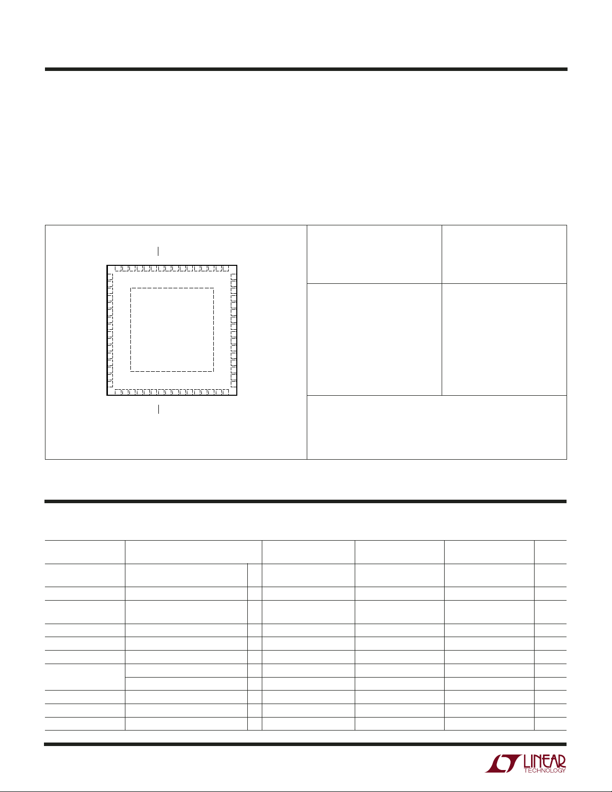
TOP VIEW
DD
64 GND
63 VDD62 SENSEA
61 VCMA
60 MODE
59 SHDNA
58 OEA
57 OFA
56 DA9
55 DA8
54 DA7
53 DA6
52 DA5
51 DA4
50 OGND
49 OV
1
A
INA+
–
A
2
INA
REFHA 3
REFHA 4
REFLA 5
REFLA 6
V
7
DD
CLKA
8
CLKB 9
V
10
DD
REFLB 11
REFLB 12
REFHB 13
REFHB 14
–
A
15
INB
+
16
A
INB
19
17
18
DD
V
GND
SENSEB
64-LEAD (9mm × 9mm) PLASTIC QFN
EXPOSED PAD (PIN 65) IS GND AND MUST BE SOLDERED TO PCB
T
65
20
NC 24
OEB 23
MUX 21
VCMB
SHDNB 22
UP PACKAGE
= 125°C, θJA = 20°C/W
JMAX
NC 25
NC 26
NC 27
DB0 28
DB1 29
DB2 30
OGND 31
48 DA3
47 DA2
46 DA1
45 DA0
44 NC
43 NC
42 NC
41 NC
40 OFB
39 DB9
38 DB8
37 DB7
36 DB6
35 DB5
34 DB4
33 DB3
32
DD
OV
Power Dissipation............................................ 1500mW
Operating Temperature Range
LTC2288C, LTC2287C, LTC2286C........... 0°C to 70°C
LTC2288I, LTC2287I, LTC2286I ..........–40°C to 85°C
Storage Temperature Range ..................–65°C to 125°C
ORDER PART
NUMBER
LTC2288CUP
LTC2288IUP
LTC2287CUP
LTC2287IUP
LTC2286CUP
LTC2286IUP
Order Options Tape and Reel: Add #TR
Lead Free: Add #PBF Lead Free Tape and Reel: Add #TRPBF
Lead Free Part Marking: http://www.linear.com/leadfree/
QFN PART*
MARKING
LTC2288UP
LTC2288UP
LTC2287UP
LTC2287UP
LTC2286UP
LTC2286UP
Consult LTC Marketing for parts specified with wider operating temperature ranges.
*The temperature grade is identified by a label on the shipping container.
U
CO VERTER CHARACTERISTICS
temperature range, otherwise specifications are at T
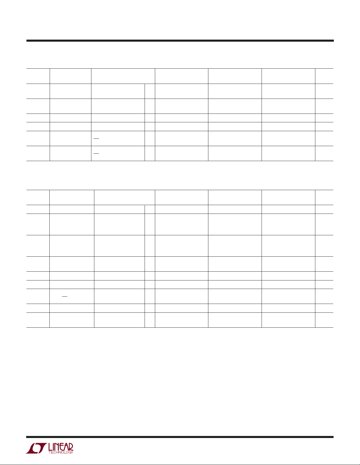
PARAMETER CONDITIONS MIN TYP MAX MIN TYP MAX MIN TYP MAX UNITS
Resolution
(No Missing Codes)
Integral Linearity Error Differential Analog Input (Note 5)
Differential Differential Analog Input
Linearity Error
Offset Error (Note 6)
Gain Error External Reference
Offset Drift ±10 ±10 ±10 µV/°C
Full-Scale Drift Internal Reference ±30 ±30 ±30 ppm/°C
External Reference ±5 ±5 ±5 ppm/°C
Gain Matching External Reference ±0.3 ±0.3 ±0.3 %FS
Offset Matching ±2 ±2 ±2mV
Transition Noise SENSE = 1V 0.07 0.07 0.07 LSB
The ● denotes the specifications which apply over the full operating
= 25°C. (Note 4)
A
LTC2288 LTC2287 LTC2286
●
10 10 10 Bits
●
–0.6 ±0.1 0.6 –0.6 ±0.1 0.6 – 0.6 ±0.1 0.6 LSB
●
–0.5 ±0.05 0.5 –0.5 ±0.05 0.5 –0.5 ±0.05 0.5 LSB
●
–12 ±212–12±212–12±212 mV
●
–2.5 ±0.5 2.5 –2.5 ±0.5 2.5 – 2.5 ±0.5 2.5 %FS
RMS
228876fa
2
Page 3
LTC2288/LTC2287/LTC2286
UU
A ALOG I PUT
specifications are at T
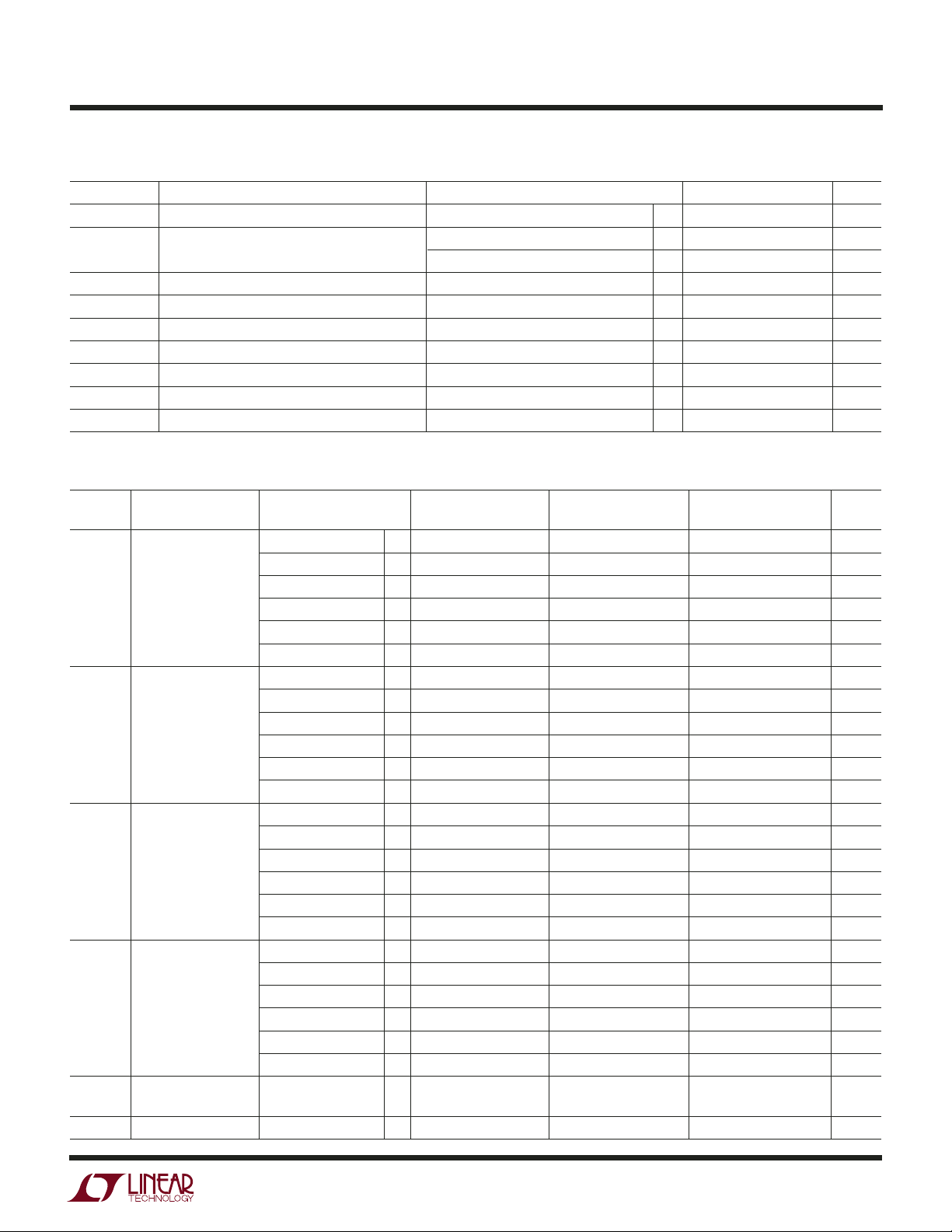
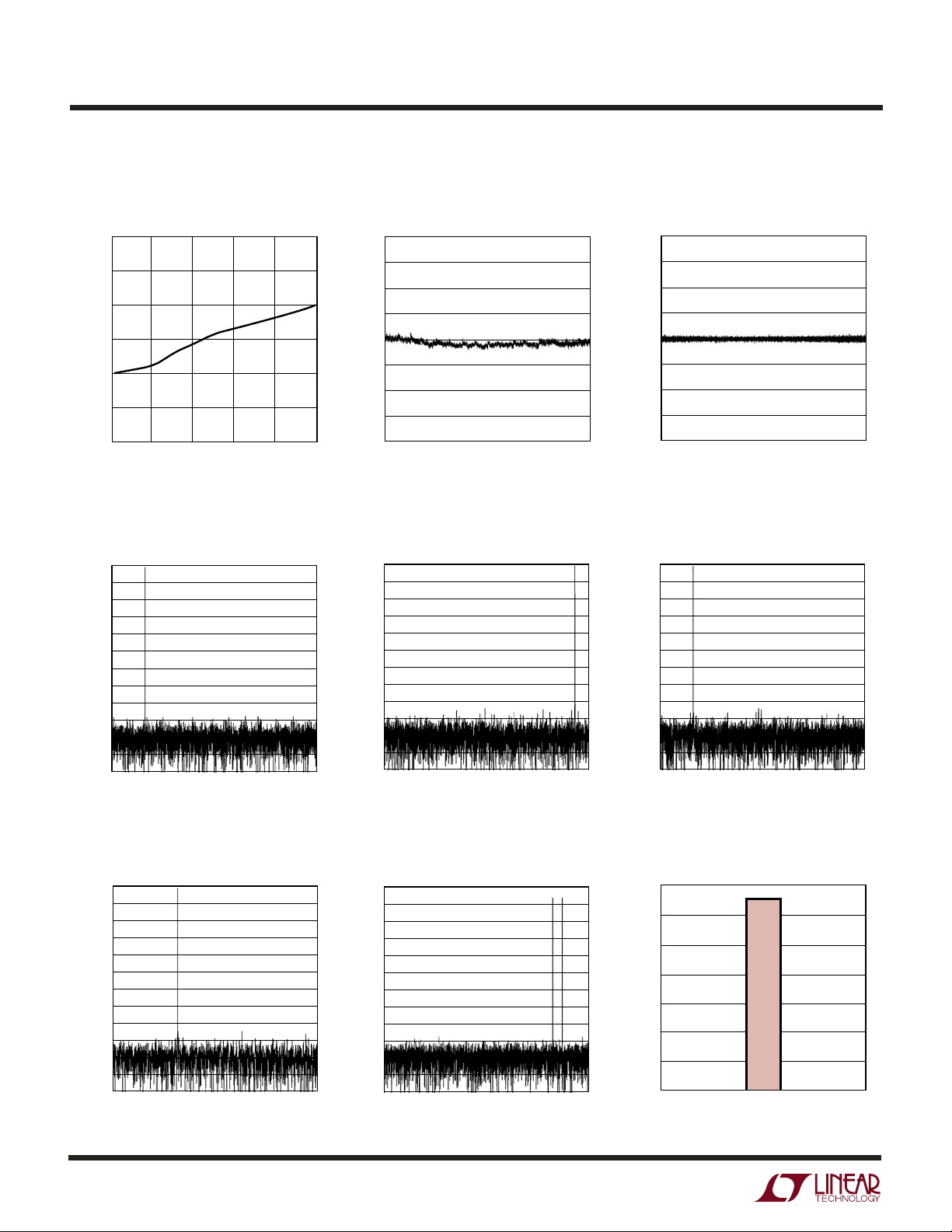
SYMBOL PARAMETER CONDITIONS MIN TYP MAX UNITS
V
IN
V
IN,CM
I
IN
I
SENSE
I
MODE
t
AP
t
JITTER
CMRR Analog Input Common Mode Rejection Ratio 80 dB
U
A
Analog Input Range (A
Analog Input Common Mode (A
Analog Input Leakage Current 0V < A
SENSEA, SENSEB Input Leakage 0V < SENSEA, SENSEB < 1V
MODE Input Leakage Current 0V < MODE < V
Sample-and-Hold Acquisition Delay Time 0 ns
Sample-and-Hold Acquisition Delay Time Jitter 0.2 ps
Full Power Bandwidth Figure 8 Test Circuit 575 MHz
W
DY A IC ACCURACY
otherwise specifications are at T
SYMBOL PARAMETER CONDITIONS MIN TYP MAX MIN TYP MAX MIN TYP MAX UNITS
SNR Signal-to-Noise Ratio 5MHz Input 61.8 61.8 61.8 dB
SFDR 5MHz Input 85 85 85 dB
SFDR 5MHz Input 85 85 85 dB
S/(N+D) 5MHz Input 61.8 61.8 61.8 dB
I
MD
Spurious Free
Dynamic Range
2nd or 3rd
Harmonic
Spurious Free
Dynamic Range
4th Harmonic
or Higher
Signal-to-Noise
Plus Distortion
Ratio
Intermodulation
Distortion
Crosstalk fIN = Nyquist –110 –110 –110 dB
The ● denotes the specifications which apply over the full operating temperature range, otherwise
= 25°C. (Note 4)
+
–
–A
IN
) 2.7V < V
IN
+
–
+A
)/2 Differential Input (Note 7)
IN
IN
Single Ended Input (Note 7)
< 3.4V (Note 7)
DD
+
–
, A
< V
IN
IN
DD
DD
●
●
●
●
●
●
±0.5 to ±1V
1 1.5 1.9 V
0.5 1.5 2 V
–1 1 µA
–3 3 µA
–3 3 µA
The ● denotes the specifications which apply over the full operating temperature range,
= 25°C. AIN = –1dBFS. (Note 4)
A
LTC2288 LTC2287 LTC2286
12.5MHz Input
20MHz Input
30MHz Input
70MHz Input 61.7 61.7 61.6 dB
140MHz Input 61.6 61.6 61.6 dB
12.5MHz Input
20MHz Input
30MHz Input
70MHz Input 85 85 85 dB
140MHz Input 80 80 80 dB
12.5MHz Input
20MHz Input
30MHz Input
70MHz Input 85 85 85 dB
140MHz Input 85 85 85 dB
12.5MHz Input
20MHz Input
30MHz Input
70MHz Input 61.7 61.6 61.6 dB
140MHz Input 61.6 61.6 61.5 dB
fIN = Nyquist, 85 85 85 dB
Nyquist + 1MHz
●
●
●
60 61.8 dB
●
●
●
69 85 dB
●
●
●
74 85 dB
●
●
●
60 61.8 dB
60 61.8 dB
69 85 dB
74 85 dB
60 61.7 dB
60 61.8 dB
69 85 dB
74 85 dB
60 61.8 dB
RMS
228876fa
3
Page 4
LTC2288/LTC2287/LTC2286
UU U
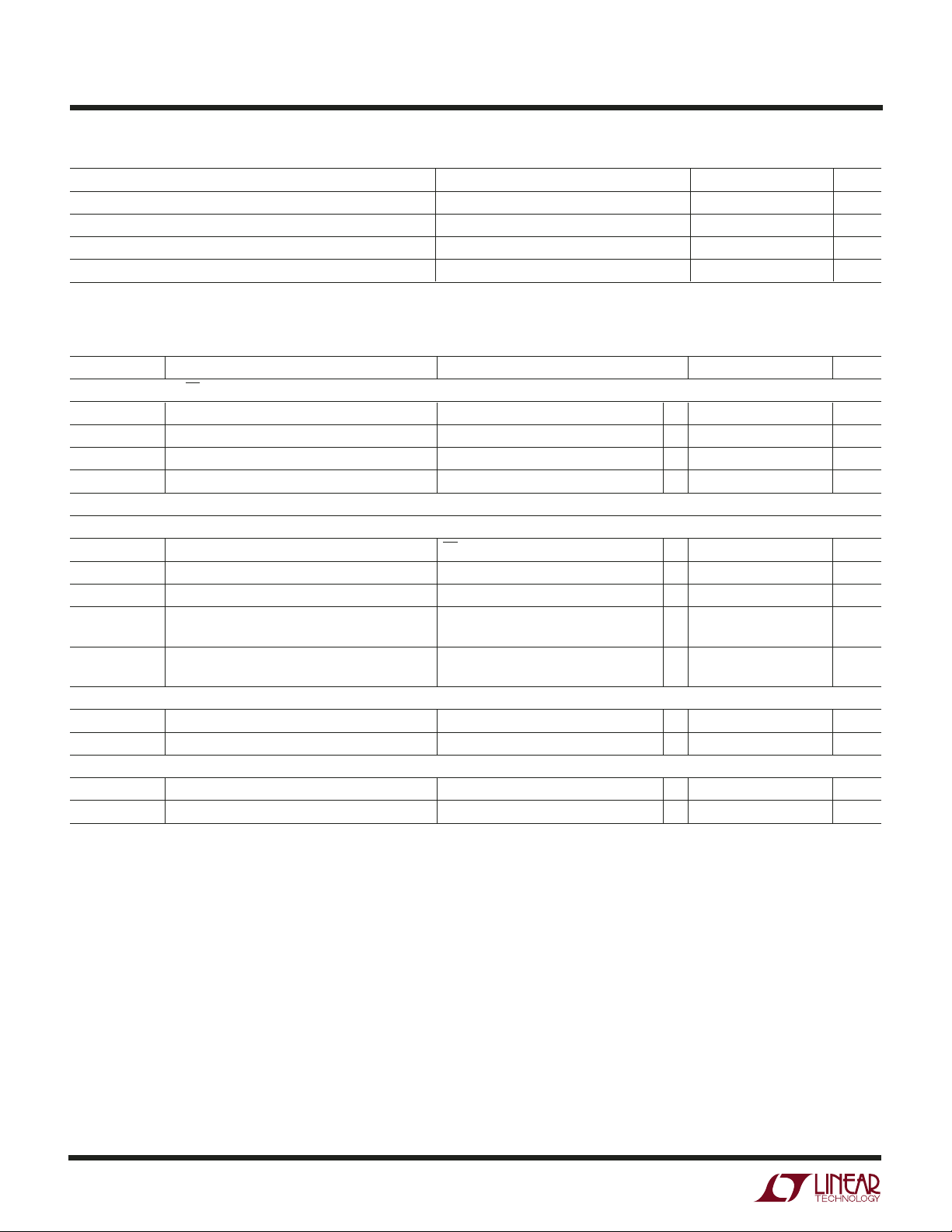
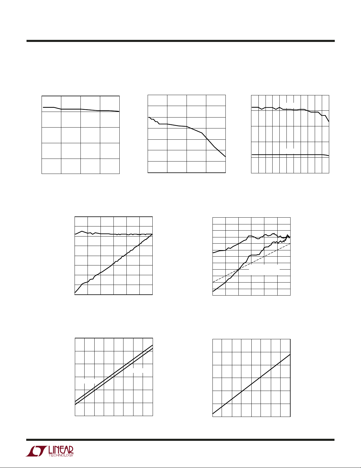
I TER AL REFERE CE CHARACTERISTICS
PARAMETER CONDITIONS MIN TYP MAX UNITS
VCM Output Voltage I
VCM Output Tempco ±25 ppm/°C
VCM Line Regulation 2.7V < VDD < 3.3V 3 mV/V
VCM Output Resistance –1mA < I
= 0 1.475 1.500 1.525 V
OUT
(Note 4)
< 1mA 4 Ω
OUT
UU
DIGITAL I PUTS A D DIGITAL OUTPUTS
full operating temperature range, otherwise specifications are at T
SYMBOL PARAMETER CONDITIONS MIN TYP MAX UNITS
LOGIC INPUTS (CLK, OE, SHDN, MUX)
V
IH
V
IL
I
IN
C
IN
LOGIC OUTPUTS
OVDD = 3V
C
OZ
I
SOURCE
I
SINK
V
OH
V
OL
OV
= 2.5V
DD
V
OH
V
OL
OVDD = 1.8V
V
OH
V
OL
High Level Input Voltage VDD = 3V
Low Level Input Voltage VDD = 3V
Input Current VIN = 0V to V
Input Capacitance (Note 7) 3 pF
Hi-Z Output Capacitance OE = High (Note 7) 3 pF
Output Source Current V
Output Sink Current V
High Level Output Voltage IO = –10µA 2.995 V
Low Level Output Voltage IO = 10µA 0.005 V
High Level Output Voltage IO = –200µA 2.49 V
Low Level Output Voltage IO = 1.6mA 0.09 V
High Level Output Voltage IO = –200µA 1.79 V
Low Level Output Voltage IO = 1.6mA 0.09 V
= 25°C. (Note 4)
A
= 0V 50 mA
OUT
= 3V 50 mA
OUT
= –200µA
I
O
= 1.6mA
I
O
The ● denotes the specifications which apply over the
●
2V
DD
●
●
–10 10 µA
●
2.7 2.99 V
●
0.09 0.4 V
0.8 V
4
228876fa
Page 5
LTC2288/LTC2287/LTC2286
WU
POWER REQUIRE E TS
range, otherwise specifications are at T
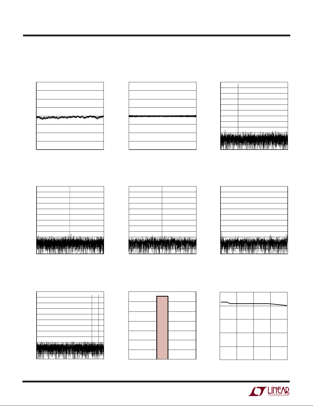
SYMBOL PARAMETER CONDITIONS MIN TYP MAX MIN TYP MAX MIN TYP MAX UNITS
V
OV
IV
P
P
P
DD
DD
DD
DISS
SHDN
NAP
Analog Supply (Note 9)
Voltage
Output Supply (Note 9)
Voltage
Supply Current Both ADCs at f
Power Dissipation Both ADCs at f
Shutdown Power SHDN = H, 2 2 2 mW
(Each Channel) OE = H, No CLK
Nap Mode Power SHDN = H, 15 15 15 mW
(Each Channel) OE = L, No CLK
= 25°C. (Note 8)
A
The ● denotes the specifications which apply over the full operating temperature
LTC2288 LTC2287 LTC2286
●
2.7 3 3.4 2.7 3 3.4 2.7 3 3.4 V
●
0.5 3 3.6 0.5 3 3.6 0.5 3 3.6 V
S(MAX)
S(MAX)
●
●
133 150 78 95 50 60 mA
400 450 235 285 150 180 mW
UW
TI I G CHARACTERISTICS
range, otherwise specifications are at T
SYMBOL PARAMETER CONDITIONS MIN TYP MAX MIN TYP MAX MIN TYP MAX UNITS
f
s
t
L
t
H
t
AP
t
D
t
MD
Pipeline 5 5 5 Cycles
Latency
Sampling Frequency (Note 9)
CLK Low Time Duty Cycle Stabilizer Off
Duty Cycle Stabilizer On
(Note 7)
CLK High Time Duty Cycle Stabilizer Off
Duty Cycle Stabilizer On
(Note 7)
Sample-and-Hold 0 0 0 ns
Aperture Delay
CLK to DATA Delay CL = 5pF (Note 7)
MUX to DATA Delay CL = 5pF (Note 7)
Data Access Time CL = 5pF (Note 7)
After OE↓
BUS Relinquish Time (Note 7)
= 25°C. (Note 4)
A
The ● denotes the specifications which apply over the full operating temperature
LTC2288 LTC2287 LTC2286
●
165140125MHz
●
7.3 7.7 500 11.8 12.5 500 18.9 20 500 ns
●
5 7.7 500 5 12.5 500 5 20 500 ns
●
7.3 7.7 500 11.8 12.5 500 18.9 20 500 ns
●
5 7.7 500 5 12.5 500 5 20 500 ns
●
1.4 2.7 5.4 1.4 2.7 5.4 1.4 2.7 5.4 ns
●
1.4 2.7 5.4 1.4 2.7 5.4 1.4 2.7 5.4 ns
●
●
4.3 10 4.3 10 4.3 10 ns
3.3 8.5 3.3 8.5 3.3 8.5 ns
Note 1: Stresses beyond those listed under Absolute Maximum Ratings
may cause permanent damage to the device. Exposure to any Absolute
Maximum Rating condition for extended periods may affect device
reliability and lifetime.
Note 2: All voltage values are with respect to ground with GND and OGND
wired together (unless otherwise noted).
Note 3: When these pin voltages are taken below GND or above V
will be clamped by internal diodes. This product can handle input currents
of greater than 100mA below GND or above VDD without latchup.
Note 4: V
25MHz (LTC2286), input range = 2V
otherwise noted.
= 3V, f
DD
= 65MHz (LTC2288), 40MHz (LTC2287), or
SAMPLE
with differential drive, unless
P-P
DD
, they
Note 5: Integral nonlinearity is defined as the deviation of a code from a
straight line passing through the actual endpoints of the transfer curve.
The deviation is measured from the center of the quantization band.
Note 6: Offset error is the offset voltage measured from –0.5 LSB when
the output code flickers between 00 0000 0000 and 11 1111 1111.
Note 7: Guaranteed by design, not subject to test.
Note 8: V
25MHz (LTC2286), input range = 1V
current and power dissipation are the sum total for both channels with
both channels active.
Note 9: Recommended operating conditions.
= 3V, f
DD
= 65MHz (LTC2288), 40MHz (LTC2287), or
SAMPLE
with differential drive. The supply
P-P
228876fa
5
Page 6
LTC2288/LTC2287/LTC2286
CODE
70000
60000
50000
40000
30000
20000
10000
0
512
65520
513
228876 G09
511
0
0
COUNT
UW
TYPICAL PERFOR A CE CHARACTERISTICS
LTC2288/LTC2287/LTC2286:
Crosstalk vs Input Frequency
–100
–105
–110
–115
CROSSTALK (dB)
–120
–125
–130
0
20 40 60 80
INPUT FREQUENCY (MHz)
LTC2288: 8192 Point FFT,
f
= 5MHz, –1dB, 2V Range,
IN
65Msps
0
–10
–20
–30
–40
–50
–60
–70
–80
AMPLITUDE (dB)
–90
–100
–110
–120
0
5
15
10
FREQUENCY (MHz)
LTC2288: 8192 Point FFT,
fIN = 140MHz, –1dB, 2V Range,
65Msps
0
–10
–20
–30
–40
–50
–60
–70
–80
AMPLITUDE (dB)
–90
–100
–110
–120
6
15
0
10
5
FREQUENCY (MHz)
LTC2288: Typical INL,
2V Range, 65Msps
1.00
0.75
0.50
0.25
0
–0.25
INL ERROR (LSB)
–0.50
–0.75
228876 G01
100
–1.00
0
256
512
CODE
768
1024
228876 G02
LTC2288: 8192 Point FFT,
fIN = 30MHz, –1dB, 2V Range,
65Msps
0
–10
–20
–30
–40
–50
–60
–70
–80
AMPLITUDE (dB)
–90
–100
–110
–120
20
25
30
228876 G04
0
10
5
FREQUENCY (MHz)
20
15
25
30
228876 G05
LTC2288: Typical DNL,
2V Range, 65Msps
1.00
0.75
0.50
0.25
0
–0.25
DNL ERROR (LSB)
–0.50
–0.75
–1.00
0
256
512
CODE
LTC2288: 8192 Point FFT,
fIN = 70MHz, –1dB, 2V Range,
65Msps
0
–10
–20
–30
–40
–50
–60
–70
–80
AMPLITUDE (dB)
–90
–100
–110
–120
0
5
15
10
FREQUENCY (MHz)
768
20
1024
22876 G03
25
30
228876 G06
LTC2288: 8192 Point 2-Tone FFT,
f
= 28.2MHz and 26.8MHz,
IN
–1dB, 2V Range 65Msps
0
–10
–20
–30
–40
–50
–60
–70
–80
AMPLITUDE (dB)
–90
–100
–110
20
25
30
228876 G07
–120
0
10
5
FREQUENCY (MHz)
25
30
228876 G08
20
15
LTC2288: Grounded Input
Histogram, 65Msps
228876fa
Page 7
LTC2288/LTC2287/LTC2286
UW
TYPICAL PERFOR A CE CHARACTERISTICS
LTC2288: SNR vs Input Frequency,
–1dB, 2V Range, 65Msps
62.5
61.5
60.5
LTC2288: SFDR vs Input Frequency,
–1dB, 2V Range, 65Msps
100
95
90
85
LTC2288: SNR and SFDR vs
Sample Rate, 2V Range,
f
= 5MHz, –1dB
IN
100
90
80
SFDR
59.5
SNR (dBFS)
58.5
57.5
0
50
INPUT FREQUENCY (MHz)
100
150
228876 G10
LTC2288: SNR vs Input Level,
= 30MHz, 2V Range, 65Msps
f
IN
80
70
60
50
40
30
SNR (dBc AND dBFS)
20
10
0
–50 –40
–60
LTC2288: I
dBFS
–30
INPUT LEVEL (dBFS)
vs Sample Rate,
VDD
5MHz Sine Wave Input, –1dB
155
200
dBc
–20
80
SFDR (dBFS)
75
70
65
0
0
–10
228876 G13
50 100 200
INPUT FREQUENCY (MHz)
150
228876 G11
LTC2288: SFDR vs Input Level,
= 30MHz, 2V Range, 65Msps
f
IN
120
110
100
90
80
70
60
50
40
SFDR (dBc AND dBFS)
30
20
10
0
–60
–50
LTC2288: I
5MHz Sine Wave Input, –1dB,
= 1.8V
O
VDD
12
70
SNR AND SFDR (dBFS)
60
50
10 20 30
0
dBFS
dBc
80dBc SFDR
REFERENCE LINE
–40 –30
INPUT LEVEL (dBFS)
OVDD
–20
vs Sample Rate,
SNR
60 70 90 100
40 50
SAMPLE RATE (Msps)
–10 0
228876 G14
80
110
228876 G12
145
135
(mA)
125
VDD
I
115
105
95
2V RANGE
0
10 30
20
40
SAMPLE RATE (Msps)
1V RANGE
50
10
8
(mA)
6
OVDD
I
4
2
70
60
80
228876 G15
0
0
10 30
20
SAMPLE RATE (Msps)
70
40
60
50
228876 G16
80
228876fa
7
Page 8
LTC2288/LTC2287/LTC2286
UW
TYPICAL PERFOR A CE CHARACTERISTICS
LTC2287: Typical INL,
2V Range, 40Msps
1.00
0.75
0.50
0.25
0
–0.25
INL ERROR (LSB)
–0.50
–0.75
–1.00
0
256
512
CODE
LTC2287: 8192 Point FFT,
f
= 30MHz, –1dB, 2V Range,
IN
40Msps
0
–10
–20
–30
–40
–50
–60
–70
AMPLITUDE (dB)
–80
–90
–100
–110
–120
0
5
10
FREQUENCY (MHz)
LTC2287: 8192 Point 2-Tone FFT,
= 21.6MHz and 23.6MHz,
f
IN
–1dB, 2V Range, 40Msps
0
–10
–20
–30
–40
–50
–60
–70
AMPLITUDE (dB)
–80
–90
–100
–110
–120
0
5
10
FREQUENCY (MHz)
768
15
15
1024
228876 G17
20
228876 G20
20
228876 G23
LTC2287: Typical DNL,
2V Range, 40Msps
1.00
0.75
0.50
0.25
0
–0.25
DNL ERROR (LSB)
–0.50
–0.75
–1.00
0
256
LTC2287: 8192 Point FFT,
f
= 70MHz, –1dB, 2V Range,
IN
40Msps
0
–10
–20
–30
–40
–50
–60
–70
AMPLITUDE (dB)
–80
–90
–100
–110
–120
0
5
FREQUENCY (MHz)
LTC2287: Grounded Input
Histogram, 40Msps
70000
60000
50000
40000
COUNT
30000
20000
10000
0
0
510
512
CODE
10
65520
511
CODE
768
15
0
512
228876 G18
228876 G21
228876 G24
1024
20
LTC2287: 8192 Point FFT,
f
= 5MHz, –1dB, 2V Range,
IN
40Msps
0
–10
–20
–30
–40
–50
–60
–70
AMPLITUDE (dB)
–80
–90
–100
–110
–120
0
5
10
FREQUENCY (MHz)
LTC2287: 8192 Point FFT,
f
= 140MHz, –1dB, 2V Range,
IN
40Msps
0
–10
–20
–30
–40
–50
–60
–70
AMPLITUDE (dB)
–80
–90
–100
–110
–120
0
5
10
FREQUENCY (MHz)
LTC2287: SNR vs Input Frequency,
–1dB, 2V Range, 40Msps
62.5
61.5
60.5
59.5
SNR (dBFS)
58.5
57.5
0
50
INPUT FREQUENCY (MHz)
100
150
15
15
20
228876 G19
20
228876 G22
200
228876 G25
228876fa
8
Page 9
LTC2288/LTC2287/LTC2286
FREQUENCY (MHz)
0
AMPLITUDE (dB)
–80
–20
–10
0
4
8
10
228876 G34
–100
–110
–40
–60
–90
–30
–120
–50
–70
2
6
12
UW
TYPICAL PERFOR A CE CHARACTERISTICS
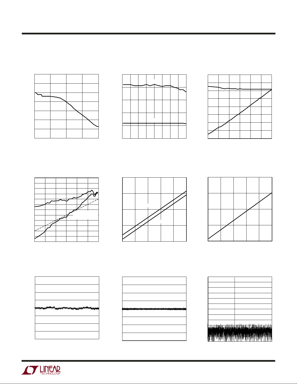
LTC2287: SNR and SFDR vs
LTC2287: SFDR vs Input Frequency,
–1dB, 2V Range, 40Msps
100
95
90
85
80
SFDR (dBFS)
75
70
65
50 100 200
0
INPUT FREQUENCY (MHz)
150
228876 G26
Sample Rate, 2V Range,
f
= 5MHz, –1dB
IN
100
90
80
70
SNR AND SFDR (dBFS)
60
50
10 20 30
0
SAMPLE RATE (Msps)
SFDR
SNR
40 50
60 70
228876 G27
80
LTC2287: SNR vs Input Level,
f
= 5MHz, 2V Range, 40Msps
IN
80
70
60
50
40
30
SNR (dBc AND dBFS)
20
10
0
–50 –40
–60
dBFS
dBc
–30
INPUT LEVEL (dBFS)
–20
–10
0
228876 G28
LTC2287: SFDR vs Input Level,
= 5MHz, 2V Range, 40Msps
f
IN
120
110
100
90
80
70
60
50
40
SFDR (dBc AND dBFS)
30
20
10
0
–60
–50
dBFS
dBc
–40 –30
INPUT LEVEL (dBFS)
LTC2286: Typical INL,
2V Range, 25Msps
1.00
0.75
0.50
0.25
0
–0.25
INL ERROR (LSB)
–0.50
–0.75
–1.00
0
256
512
CODE
80dBc SFDR
REFERENCE LINE
–20
–10 0
228876 G29
768
228876 G32
1024
LTC2287: I
vs Sample Rate,
VDD
5MHz Sine Wave Input, –1dB
100
90
(mA)
VDD
I
80
70
60
0
2V RANGE
10
20
SAMPLE RATE (Msps)
LTC2286: Typical DNL,
2V Range, 25Msps
1.00
0.75
0.50
0.25
0
–0.25
DNL ERROR (LSB)
–0.50
–0.75
–1.00
0
256
512
CODE
1V RANGE
30
768
40
228876 G30
228876 G33
50
1024
LTC2287: I
vs Sample Rate,
OVDD
5MHz Sine Wave Input, –1dB,
= 1.8V
O
VDD
8
6
(mA)
4
OVDD
I
2
0
10
0
SAMPLE RATE (Msps)
30
20
LTC2286: 8192 Point FFT,
= 5MHz, –1dB, 2V Range,
f
IN
25Msps
40
50
228876 G31
228876fa
9
Page 10
LTC2288/LTC2287/LTC2286
UW
TYPICAL PERFOR A CE CHARACTERISTICS
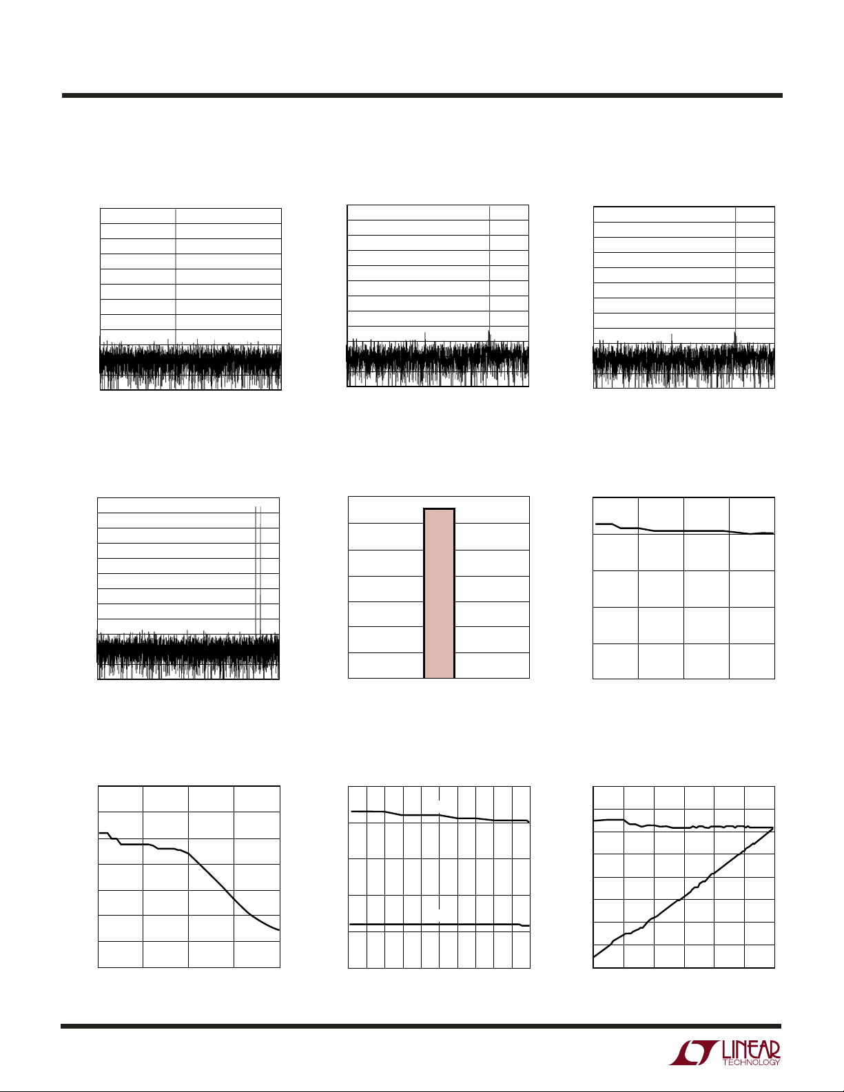
LTC2286: 8192 Point FFT,
f
= 30MHz, –1dB, 2V Range,
IN
25Msps
0
–10
–20
–30
–40
–50
–60
–70
–80
AMPLITUDE (dB)
–90
–100
–110
–120
0
4
2
FREQUENCY (MHz)
8
6
LTC2286: 8192 Point 2-Tone FFT,
f
= 10.9MHz and 13.8MHz,
IN
–1dB, 2V Range, 25Msps
0
–10
–20
–30
–40
–50
–60
–70
–80
AMPLITUDE (dB)
–90
–100
–110
–120
0
4
2
FREQUENCY (MHz)
8
6
LTC2286: SFDR vs Input
Frequency, –1dB, 2V Range,
25Msps
100
95
90
85
80
SFDR (dBFS)
75
70
65
50 100 200
0
INPUT FREQUENCY (MHz)
150
LTC2286: 8192 Point FFT,
= 70MHz, –1dB, 2V Range,
f
IN
25Msps
0
–10
–20
–30
–40
–50
–60
–70
–80
AMPLITUDE (dB)
–90
–100
–110
–120
10
12
228876 G35
0
4
2
FREQUENCY (MHz)
8
6
10
12
228876 G36
LTC2286: Grounded Input
Histogram, 25Msps
70000
60000
50000
40000
COUNT
30000
20000
10000
0
0
10
12
228876 G38
511
65520
512
CODE
0
513
228876 G39
LTC2286: 8192 Point FFT,
f
= 140MHz, –1dB, 2V Range,
IN
25Msps
0
–10
–20
–30
–40
–50
–60
–70
–80
AMPLITUDE (dB)
–90
–100
–110
–120
0
4
2
FREQUENCY (MHz)
8
6
LTC2286: SNR vs Input Frequency,
–1dB, 2V Range, 25Msps
62.5
61.5
60.5
59.5
SNR (dBFS)
58.5
57.5
0
50
INPUT FREQUENCY (MHz)
100
150
10
12
228876 G37
200
228876 G40
LTC2286: SNR and SFDR vs
LTC2286: SNR vs Input Level,
fIN = 5MHz, 2V Range, 25Msps
80
70
60
50
40
30
SNR (dBc AND dBFS)
20
10
0
–50 –40
–60
dBFS
dBc
–30
INPUT LEVEL (dBFS)
–20
–10
228876 G43
228876fa
0
228876 G41
Sample Rate, 2V Range,
= 5MHz, –1dB
f
IN
100
90
80
70
SNR AND SFDR (dBFS)
60
50
51015
0
20 25
SAMPLE RATE (Msps)
SFDR
SNR
30 35 45 50
40
228876 G42
10
Page 11
LTC2288/LTC2287/LTC2286
0
10
20
515
25
30
35
SAMPLE RATE (Msps)
I
OVDD
(mA)
228876 G46
6
4
2
0
UW
TYPICAL PERFOR A CE CHARACTERISTICS
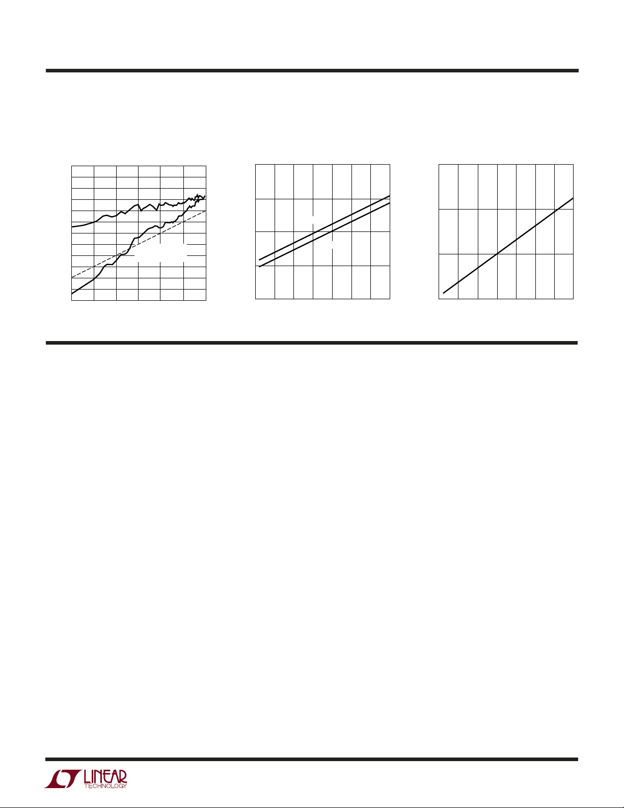
LTC2286: SFDR vs Input Level,
= 5MHz, 2V Range, 25Msps
f
IN
120
110
100
90
80
70
60
50
40
SFDR (dBc AND dBFS)
30
20
10
0
–60
–50
U
dBFS
dBc
80dBc SFDR
REFERENCE LINE
–40 –30
INPUT LEVEL (dBFS)
–20
UU
–10 0
228876 G44
70
60
(mA)
50
VDD
I
40
30
0
PI FU CTIO S
+
A
(Pin 1): Channel A Positive Differential Analog
INA
Input.
–
A
(Pin 2): Channel A Negative Differential Analog
INA
Input.
REFHA (Pins 3, 4): Channel A High Reference. Short
together and bypass to Pins 5, 6 with a 0.1µF ceramic chip
capacitor as close to the pin as possible. Also bypass to
Pins 5, 6 with an additional 2.2µF ceramic chip capacitor
and to ground with a 1µF ceramic chip capacitor.
REFLA (Pins 5, 6): Channel A Low Reference. Short
together and bypass to Pins 3, 4 with a 0.1µF ceramic chip
capacitor as close to the pin as possible. Also bypass to
Pins 3, 4 with an additional 2.2µF ceramic chip capacitor
and to ground with a 1µF ceramic chip capacitor.
VDD (Pins 7, 10, 18, 63): Analog 3V Supply. Bypass to
GND with 0.1µF ceramic chip capacitors.
CLKA (Pin 8): Channel A Clock Input. The input sample
starts on the positive edge.
CLKB (Pin 9): Channel B Clock Input. The input sample
starts on the positive edge.
REFLB (Pins 11, 12): Channel B Low Reference. Short
together and bypass to Pins 13, 14 with a 0.1µF ceramic
LTC2286: I
vs Sample Rate,
VDD
5MHz Sine Wave Input, –1dB
2V RANGE
1V RANGE
25
515
10
SAMPLE RATE (Msps)
20
chip capacitor as close to the pin as possible. Also bypass
to Pins 13, 14 with an additional 2.2µF ceramic chip ca-
pacitor and to ground with a 1µF ceramic chip capacitor.
REFHB (Pins 13, 14): Channel B High Reference. Short
together and bypass to Pins 11, 12 with a 0.1µF ceramic
chip capacitor as close to the pin as possible. Also bypass
to Pins 11, 12 with an additional 2.2µF ceramic chip ca-
pacitor and to ground with a 1µF ceramic chip capacitor.
–
A
(Pin 15): Channel B Negative Differential Analog
INB
Input.
+
A
(Pin 16): Channel B Positive Differential Analog
INB
Input.
GND (Pins 17, 64): ADC Power Ground.
SENSEB (Pin 19): Channel B Reference Programming Pin.
Connecting SENSEB to V
and a ±0.5V input range. V
and a ±1V input range. An external reference greater than
0.5V and less than 1V applied to SENSEB selects an input
range of ±V
V
(Pin 20): Channel B 1.5V Output and Input Common
CMB
Mode Bias. Bypass to ground with 2.2µF ceramic chip
capacitor. Do not connect to V
30
228876 G45
SENSEB
LTC2286: I
vs Sample Rate,
OVDD
5MHz Sine Wave Input, –1dB,
O
= 1.8V
VDD
35
selects the internal reference
CMB
selects the internal reference
DD
. ±1V is the largest valid input range.
.
CMA
228876fa
11
Page 12

LTC2288/LTC2287/LTC2286
U
UU
PI FU CTIO S
MUX (Pin 21): Digital Output Multiplexer Control. If MUX
is High, Channel A comes out on DA0-DA9, OFA; Channel B
comes out on DB0-DB9, OFB. If MUX is Low, the output
busses are swapped and Channel A comes out on DB0DB9, OFB; Channel B comes out on DA0-DA9, OFA. To
multiplex both channels onto a single output bus, connect
MUX, CLKA and CLKB together.
SHDNB (Pin 22): Channel B Shutdown Mode Selection
Pin. Connecting SHDNB to GND and OEB to GND results
in normal operation with the outputs enabled. Connecting
SHDNB to GND and OEB to V
tion with the outputs at high impedance. Connecting
SHDNB to V
the outputs at high impedance. Connecting SHDNB to V
and OEB to VDD results in sleep mode with the outputs at
high impedance.
OEB (Pin 23): Channel B Output Enable Pin. Refer to
SHDNB pin function.
NC (Pins 24 to 27, 41 to 44): Do Not Connect These Pins.
DB0 – DB9 (Pins 28 to 30, 33 to 39): Channel B Digital
Outputs. DB9 is the MSB.
OGND (Pins 31, 50): Output Driver Ground.
(Pins 32, 49): Positive Supply for the Output Driv-
OV
DD
ers. Bypass to ground with 0.1µF ceramic chip capacitor.
OFB (Pin 40): Channel B Overflow/Underflow Output.
High when an overflow or underflow has occurred.
DA0 – DA9 (Pins 45 to 48, 51 to 56): Channel A Digital
Outputs. DA9 is the MSB.
OFA (Pin 57): Channel A Overflow/Underflow Output.
High when an overflow or underflow has occurred.
and OEB to GND results in nap mode with
DD
results in normal opera-
DD
DD
SHDNA (Pin 59): Channel A Shutdown Mode Selection
Pin. Connecting SHDNA to GND and OEA to GND results
in normal operation with the outputs enabled. Connecting
SHDNA to GND and OEA to VDD results in normal operation with the outputs at high impedance. Connecting
SHDNA to V
the outputs at high impedance. Connecting SHDNA to V
and OEA to VDD results in sleep mode with the outputs at
high impedance.
MODE (Pin 60): Output Format and Clock Duty Cycle
Stabilizer Selection Pin. Note that MODE controls both
channels. Connecting MODE to GND selects offset binary
output format and turns the clock duty cycle stabilizer off.
1/3 V
DD
clock duty cycle stabilizer on. 2/3 V
ment output format and turns the clock duty cycle stabilizer on. V
turns the clock duty cycle stabilizer off.
V
(Pin 61): Channel A 1.5V Output and Input Common
CMA
Mode Bias. Bypass to ground with 2.2µF ceramic chip
capacitor. Do not connect to V
SENSEA (Pin 62): Channel A Reference Programming Pin.
Connecting SENSEA to V
and a ±0.5V input range. V
and a ±1V input range. An external reference greater than
0.5V and less than 1V applied to SENSEA selects an input
range of ±V
GND (Exposed Pad) (Pin 65): ADC Power Ground. The
Exposed Pad on the bottom of the package needs to be
soldered to ground.
and OEA to GND results in nap mode with
DD
DD
selects offset binary output format and turns the
selects 2’s comple-
DD
selects 2’s complement output format and
DD
.
CMB
selects the internal reference
CMA
selects the internal reference
DD
SENSEA
. ±1V is the largest valid input range.
OEA (Pin 58): Channel A Output Enable Pin. Refer to
SHDNA pin function.
12
228876fa
Page 13
LTC2288/LTC2287/LTC2286
UU
W
FUNCTIONAL BLOCK DIAGRA
+
A
IN
A
V
2.2µF
SENSE
INPUT
S/H
–
IN
CM
1.5V
REFERENCE
RANGE
SELECT
FIRST PIPELINED
ADC STAGE
REF
BUF
SECOND PIPELINED
ADC STAGE
DIFF
REF
AMP
REFH
0.1µF
2.2µF
THIRD PIPELINED
ADC STAGE
INTERNAL CLOCK SIGNALSREFH REFL
REFL
FOURTH PIPELINED
CLOCK/DUTY
CYCLE
CONTROL
CLK
ADC STAGE
CONTROL
LOGIC
SHDN
FIFTH PIPELINED
ADC STAGE
OEMODE
SIXTH PIPELINED
ADC STAGE
SHIFT REGISTER
AND CORRECTION
OUTPUT
DRIVERS
OGND
228876 F01
OV
DD
OF
D9
•
•
•
D0
1µF1µF
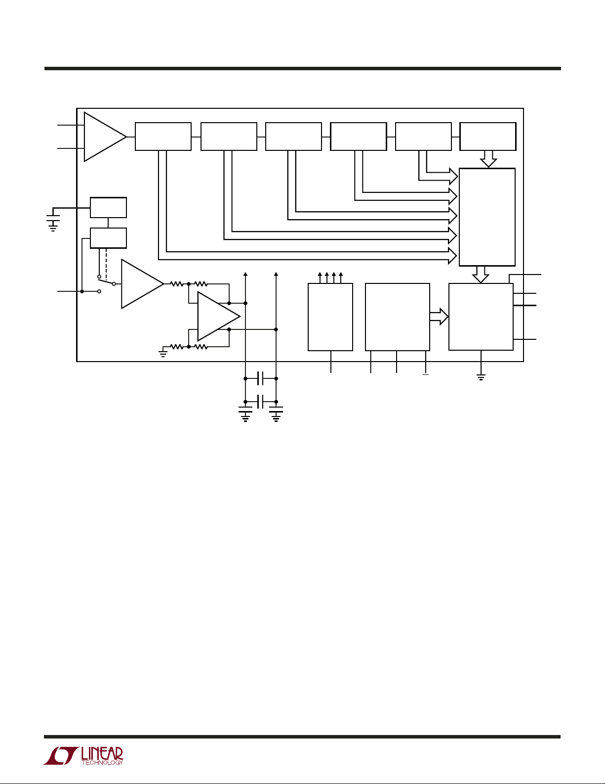
Figure 1. Functional Block Diagram (Only One Channel is Shown)
228876fa
13
Page 14
LTC2288/LTC2287/LTC2286
WUW
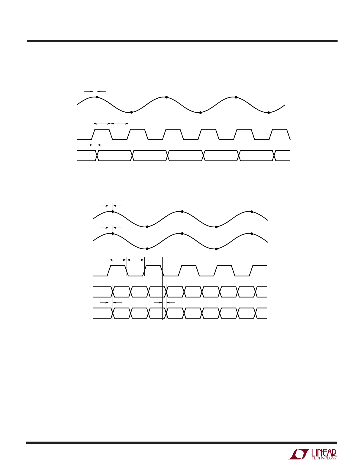
TI I G DIAGRA S
Dual Digital Output Bus Timing
(Only One Channel is Shown)
t
AP
ANALOG
INPUT
N
N + 1
N + 2
N + 3
N + 4
N + 5
CLK
D0-D9, OF
ANALOG
INPUT A
ANALOG
INPUT B
CLKA = CLKB = MUX
D0A-D9A, OFA
t
t
H
L
t
D
N – 5
N – 4 N – 3 N – 2 N – 1
N
228876 TD01
Multiplexed Digital Output Bus Timing
t
APA
B – 4
A + 2
B + 2
t
MD
A – 3
B – 3
A + 3
B + 3
A – 2
A
t
APB
B
t
H
A – 5
t
D
t
L
B – 5
A + 1
B + 1
A – 4
B – 2
A + 4
B + 4
A – 1
14
D0B-D9B, OFB
B – 5
A – 5
B – 4
A – 4
B – 3
A – 3
B – 2
A – 2
B – 1
228876 TD02
228876fa
Page 15

WUUU
APPLICATIO S I FOR ATIO
LTC2288/LTC2287/LTC2286
DYNAMIC PERFORMANCE
Signal-to-Noise Plus Distortion Ratio
The signal-to-noise plus distortion ratio [S/(N + D)] is the
ratio between the RMS amplitude of the fundamental input
frequency and the RMS amplitude of all other frequency
components at the ADC output. The output is band limited
to frequencies above DC to below half the sampling
frequency.
Signal-to-Noise Ratio
The signal-to-noise ratio (SNR) is the ratio between the
RMS amplitude of the fundamental input frequency and
the RMS amplitude of all other frequency components
except the first five harmonics and DC.
Total Harmonic Distortion
Total harmonic distortion is the ratio of the RMS sum of all
harmonics of the input signal to the fundamental itself. The
out-of-band harmonics alias into the frequency band
between DC and half the sampling frequency. THD is
expressed as:
2fb + fa, 2fa – fb and 2fb – fa. The intermodulation
distortion is defined as the ratio of the RMS value of either
input tone to the RMS value of the largest 3rd order
intermodulation product.
Spurious Free Dynamic Range (SFDR)
Spurious free dynamic range is the peak harmonic or
spurious noise that is the largest spectral component
excluding the input signal and DC. This value is expressed
in decibels relative to the RMS value of a full scale input
signal.
Input Bandwidth
The input bandwidth is that input frequency at which the
amplitude of the reconstructed fundamental is reduced by
3dB for a full scale input signal.
Aperture Delay Time
The time from when CLK reaches midsupply to the instant
that the input signal is held by the sample and hold circuit.
Aperture Delay Jitter
THD = 20Log (√(V22 + V32 + V42 + . . . Vn2)/V1)
where V1 is the RMS amplitude of the fundamental frequency and V2 through Vn are the amplitudes of the
second through nth harmonics. The THD calculated in this
data sheet uses all the harmonics up to the fifth.
Intermodulation Distortion
If the ADC input signal consists of more than one spectral
component, the ADC transfer function nonlinearity can
produce intermodulation distortion (IMD) in addition to
THD. IMD is the change in one sinusoidal input caused by
the presence of another sinusoidal input at a different
frequency.
If two pure sine waves of frequencies fa and fb are applied
to the ADC input, nonlinearities in the ADC transfer function can create distortion products at the sum and difference frequencies of mfa ± nfb, where m and n = 0, 1, 2, 3,
etc. The 3rd order intermodulation products are 2fa + fb,
The variation in the aperture delay time from conversion to
conversion. This random variation will result in noise
when sampling an AC input. The signal to noise ratio due
to the jitter alone will be:
SNR
Crosstalk
Crosstalk is the coupling from one channel (being driven
by a full-scale signal) onto the other channel (being driven
by a –1dBFS signal).
CONVERTER OPERATION
As shown in Figure 1, the LTC2288/LTC2287/LTC2286 are
dual CMOS pipelined multistep converters. The converters have six pipelined ADC stages; a sampled analog input
will result in a digitized value five cycles later (see the
Timing Diagram section). For optimal AC performance the
analog inputs should be driven differentially. For cost
= –20log (2π • fIN • t
JITTER
JITTER
)
228876fa
15
Page 16
LTC2288/LTC2287/LTC2286
U
WUU
APPLICATIO S I FOR ATIO
sensitive applications, the analog inputs can be driven
single-ended with slightly worse harmonic distortion. The
CLK input is single-ended. The LTC2288/LTC2287/
LTC2286 have two phases of operation, determined by the
state of the CLK input pin.
Each pipelined stage shown in Figure 1 contains an ADC,
a reconstruction DAC and an interstage residue amplifier.
In operation, the ADC quantizes the input to the stage and
the quantized value is subtracted from the input by the
DAC to produce a residue. The residue is amplified and
output by the residue amplifier. Successive stages operate
out of phase so that when the odd stages are outputting
their residue, the even stages are acquiring that residue
and vice versa.
When CLK is low, the analog input is sampled differentially
directly onto the input sample-and-hold capacitors, inside
the “Input S/H” shown in the block diagram. At the instant
that CLK transitions from low to high, the sampled input is
held. While CLK is high, the held input voltage is buffered
by the S/H amplifier which drives the first pipelined ADC
stage. The first stage acquires the output of the S/H during
this high phase of CLK. When CLK goes back low, the first
stage produces its residue which is acquired by the
second stage. At the same time, the input S/H goes back
to acquiring the analog input. When CLK goes back high,
the second stage produces its residue which is acquired
by the third stage. An identical process is repeated for the
third, fourth and fifth stages, resulting in a fifth stage
residue that is sent to the sixth stage ADC for final
evaluation.
Each ADC stage following the first has additional range to
accommodate flash and amplifier offset errors. Results
from all of the ADC stages are digitally synchronized such
that the results can be properly combined in the correction
logic before being sent to the output buffer.
SAMPLE/HOLD OPERATION AND INPUT DRIVE
Sample/Hold Operation
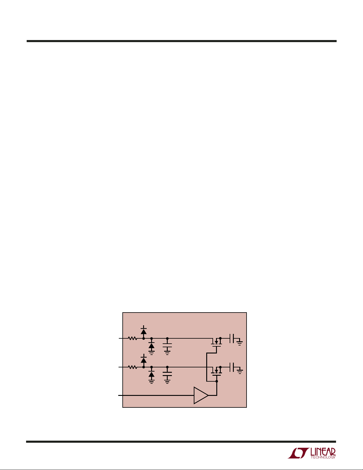
Figure 2 shows an equivalent circuit for the LTC2288/
LTC2287/LTC2286 CMOS differential sample-and-hold.
The analog inputs are connected to the sampling capacitors (C
SAMPLE
shown attached to each input (C
) through NMOS transistors. The capacitors
PARASITIC
) are the summa-
tion of all other capacitance associated with each input.
During the sample phase when CLK is low, the transistors
connect the analog inputs to the sampling capacitors and
they charge to and track the differential input voltage.
When CLK transitions from low to high, the sampled input
voltage is held on the sampling capacitors. During the hold
phase when CLK is high, the sampling capacitors are
disconnected from the input and the held voltage is passed
to the ADC core for processing. As CLK transitions from
high to low, the inputs are reconnected to the sampling
16
LTC2288/LTC2287/LTC2286
15Ω
+
A
IN
15Ω
–
A
IN
CLK
V
DD
C
PARASITIC
V
DD
Figure 2. Equivalent Input Circuit
1pF
C
PARASITIC
1pF
V
DD
C
SAMPLE
4pF
C
SAMPLE
4pF
228876 F02
228876fa
Page 17
WUUU
APPLICATIO S I FOR ATIO
LTC2288/LTC2287/LTC2286
capacitors to acquire a new sample. Since the sampling
capacitors still hold the previous sample, a charging glitch
proportional to the change in voltage between samples will
be seen at this time. If the change between the last sample
and the new sample is small, the charging glitch seen at
the input will be small. If the input change is large, such as
the change seen with input frequencies near Nyquist, then
a larger charging glitch will be seen.
Single-Ended Input
For cost sensitive applications, the analog inputs can be
driven single-ended. With a single-ended input the harmonic distortion and INL will degrade, but the SNR and
DNL will remain unchanged. For a single-ended input, A
should be driven with the input signal and A
connected to 1.5V or V
CM
.
–
should be
IN
IN
+
Common Mode Bias
For optimal performance the analog inputs should be
driven differentially. Each input should swing ±0.5V for
the 2V range or ±0.25V for the 1V range, around a
common mode voltage of 1.5V. The V
be used to provide the common mode bias level. V
output pin may
CM
CM
can
be tied directly to the center tap of a transformer to set the
DC input level or as a reference level to an op amp
differential driver circuit. The V
pin must be bypassed to
CM
ground close to the ADC with a 2.2µF or greater capacitor.
Input Drive Impedance
As with all high performance, high speed ADCs, the
dynamic performance of the LTC2288/LTC2287/LTC2286
can be influenced by the input drive circuitry, particularly
the second and third harmonics. Source impedance and
reactance can influence SFDR. At the falling edge of CLK,
the sample-and-hold circuit will connect the 4pF sampling
capacitor to the input pin and start the sampling period.
The sampling period ends when CLK rises, holding the
sampled input on the sampling capacitor. Ideally the input
circuitry should be fast enough to fully charge
the sampling capacitor during the sampling period
1/(2F
ENCODE
); however, this is not always possible and the
incomplete settling may degrade the SFDR. The sampling
glitch has been designed to be as linear as possible to
minimize the effects of incomplete settling.
For the best performance, it is recommended to have a
source impedance of 100Ω or less for each input. The
source impedance should be matched for the differential
inputs. Poor matching will result in higher even order
harmonics, especially the second.
Input Drive Circuits
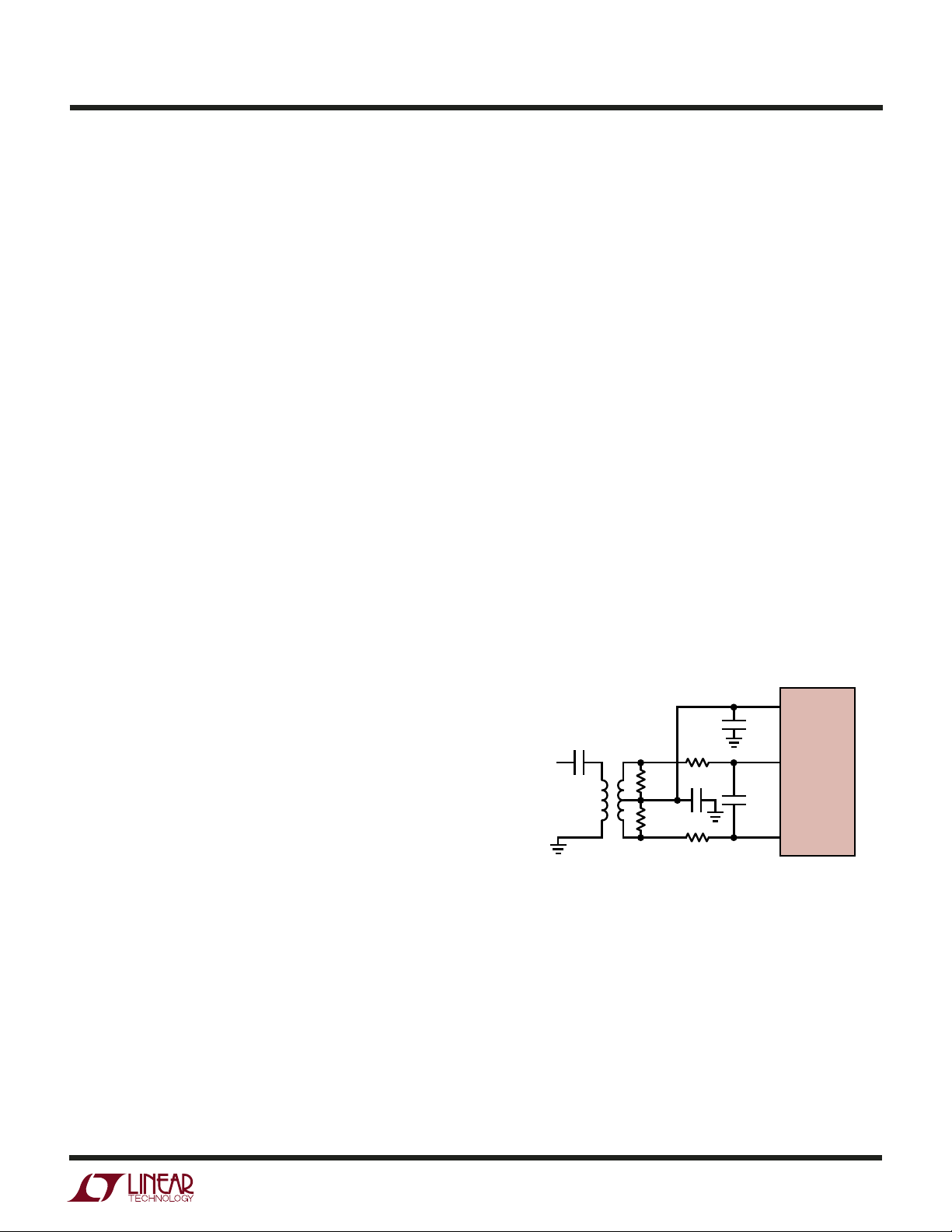
Figure 3 shows the LTC2288/LTC2287/LTC2286 being
driven by an RF transformer with a center tapped secondary. The secondary center tap is DC biased with V
CM
,
setting the ADC input signal at its optimum DC level.
Terminating on the transformer secondary is desirable, as
this provides a common mode path for charging glitches
caused by the sample and hold. Figure 3 shows a 1:1 turns
ratio transformer. Other turns ratios can be used if the
source impedance seen by the ADC does not exceed 100Ω
for each ADC input. A disadvantage of using a transformer
is the loss of low frequency response. Most small RF
transformers have poor performance at frequencies below 1MHz.
V
CM
2.2µF
0.1µFT1
ANALOG
INPUT
Figure 3. Single-Ended to Differential Conversion
Using a Transformer
1:1
T1 = MA/COM ETC1-1T
RESISTORS, CAPACITORS
ARE 0402 PACKAGE SIZE
25Ω
25Ω
25Ω
0.1µF
25Ω
12pF
+
A
IN
LTC2288
LTC2287
LTC2286
–
A
IN
228876 F03
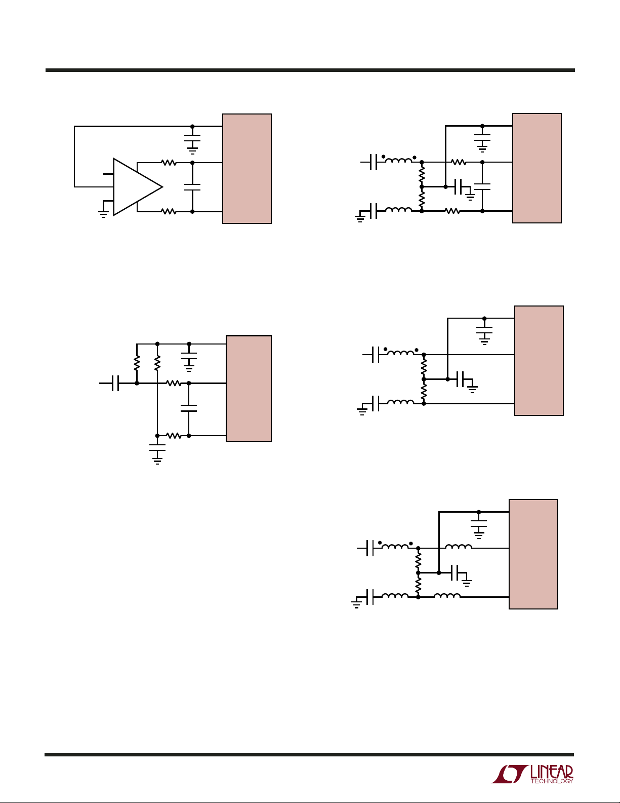
Figure 4 demonstrates the use of a differential amplifier to
convert a single ended input signal into a differential input
signal. The advantage of this method is that it provides low
frequency input response; however, the limited gain bandwidth of most op amps will limit the SFDR at high input
frequencies.
228876fa
17
Page 18
LTC2288/LTC2287/LTC2286
WUUU
APPLICATIO S I FOR ATIO
V
CM
2.2µF
A
12pF
A
+
IN
LTC2288
LTC2287
LTC2286
–
IN
228876 F04
ANALOG
INPUT
HIGH SPEED
DIFFERENTIAL
AMPLIFIER
+
+
CM
–
–
25Ω
25Ω
Figure 4. Differential Drive with an Amplifier
Figure 5 shows a single-ended input circuit. The impedance seen by the analog inputs should be matched. This
circuit is not recommended if low distortion is required.
V
CM
2.2µF
12pF
+
A
IN
LTC2288
LTC2287
LTC2286
–
A
IN
228876 F05
ANALOG
INPUT
1k
0.1µF
1k
25Ω
25Ω
0.1µF
Figure 5. Single-Ended Drive
V
CM
2.2µF
ANALOG
INPUT
0.1µF
T1
0.1µF
T1 = MA/COM, ETC 1-1-13
RESISTORS, CAPACITORS
ARE 0402 PACKAGE SIZE
25Ω
25Ω
0.1µF
12Ω
12Ω
8pF
A
IN
A
IN
Figure 6. Recommended Front End Circuit for
Input Frequencies Between 70MHz and 170MHz
V
CM
2.2µF
ANALOG
INPUT
0.1µF
T1
0.1µF
T1 = MA/COM, ETC 1-1-13
RESISTORS, CAPACITORS
ARE 0402 PACKAGE SIZE
25Ω
25Ω
0.1µF
A
IN
A
IN
Figure 7. Recommended Front End Circuit for
Input Frequencies Between 170MHz and 300MHz
+
–
+
–
LTC2288
LTC2287
LTC2286
LTC2288
LTC2287
LTC2286
228876 F06
228876 F07
The 25Ω resistors and 12pF capacitor on the analog inputs
serve two purposes: isolating the drive circuitry from the
sample-and-hold charging glitches and limiting the
wideband noise at the converter input.
For input frequencies above 70MHz, the input circuits of
Figure 6, 7 and 8 are recommended. The balun transformer gives better high frequency response than a flux
coupled center tapped transformer. The coupling capacitors allow the analog inputs to be DC biased at 1.5V. In
Figure 8, the series inductors are impedance matching
elements that maximize the ADC bandwidth.
18
ANALOG
0.1µF
INPUT
T1
0.1µF
T1 = MA/COM, ETC 1-1-13
RESISTORS, CAPACITORS, INDUCTORS
ARE 0402 PACKAGE SIZE
25Ω
25Ω
6.8nH
0.1µF
6.8nH
Figure 8. Recommended Front End Circuit for
Input Frequencies Above 300MHz
V
2.2µF
A
A
CM
+
IN
LTC2288
LTC2287
LTC2286
–
IN
228876 F08
228876fa
Page 19
V
CM
SENSE
1.5V
0.75V
2.2µF
12k
1µF
12k
228876 F10
LTC2288
LTC2287
LTC2286
WUUU
APPLICATIO S I FOR ATIO
LTC2288/LTC2287/LTC2286
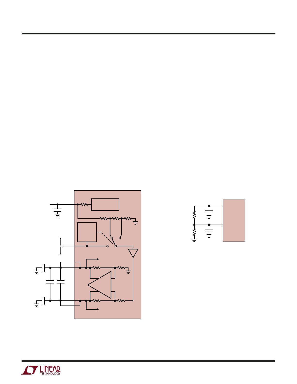
Reference Operation
Figure 9 shows the LTC2288/LTC2287/LTC2286 reference circuitry consisting of a 1.5V bandgap reference, a
difference amplifier and switching and control circuit. The
internal voltage reference can be configured for two pin
selectable input ranges of 2V (±1V differential) or 1V
(±0.5V differential). Tying the SENSE pin to VDD selects
the 2V range; tying the SENSE pin to V
selects the 1V
CM
range.
The 1.5V bandgap reference serves two functions: its
output provides a DC bias point for setting the common
mode voltage of any external input circuitry; additionally,
the reference is used with a difference amplifier to generate the differential reference levels needed by the internal
ADC circuitry. An external bypass capacitor is required for
the 1.5V reference output, V
. This provides a high
CM
frequency low impedance path to ground for internal and
external circuitry.
LTC2288/LTC2287/LTC2286
1.5V
V
2.2µF
CM
4Ω
1.5V BANDGAP
REFERENCE
1V
0.5V
The difference amplifier generates the high and low reference for the ADC. High speed switching circuits are
connected to these outputs and they must be externally
bypassed. Each output has two pins. The multiple output
pins are needed to reduce package inductance. Bypass
capacitors must be connected as shown in Figure 9. Each
ADC channel has an independent reference with its own
bypass capacitors. The two channels can be used with the
same or different input ranges.
Other voltage ranges between the pin selectable ranges
can be programmed with two external resistors as shown
in Figure 10. An external reference can be used by applying
its output directly or through a resistor divider to SENSE.
It is not recommended to drive the SENSE pin with a logic
device. The SENSE pin should be tied to the appropriate
level as close to the converter as possible. If the SENSE pin
is driven externally, it should be bypassed to ground as
close to the device as possible with a 1µF ceramic capacitor.
For the best channel matching, connect an external reference
to SENSEA and SENSEB.
TIE TO V
TIE TO V
RANGE = 2 • V
FOR 2V RANGE;
DD
FOR 1V RANGE;
CM
SENSE
0.5V < V
SENSE
1µF
2.2µF
1µF
Figure 9. Equivalent Reference Circuit
FOR
< 1V
SENSE
REFH
0.1µF
REFL
RANGE
DETECT
AND
CONTROL
INTERNAL ADC
HIGH REFERENCE
DIFF AMP
INTERNAL ADC
LOW REFERENCE
BUFFER
228876 F09
Figure 10. 1.5V Range ADC
Input Range
The input range can be set based on the application. The
2V input range will provide the best signal-to-noise performance while maintaining excellent SFDR. The 1V input
range will have better SFDR performance, but the SNR will
degrade by 0.6dB. See the Typical Performance Characteristics section.
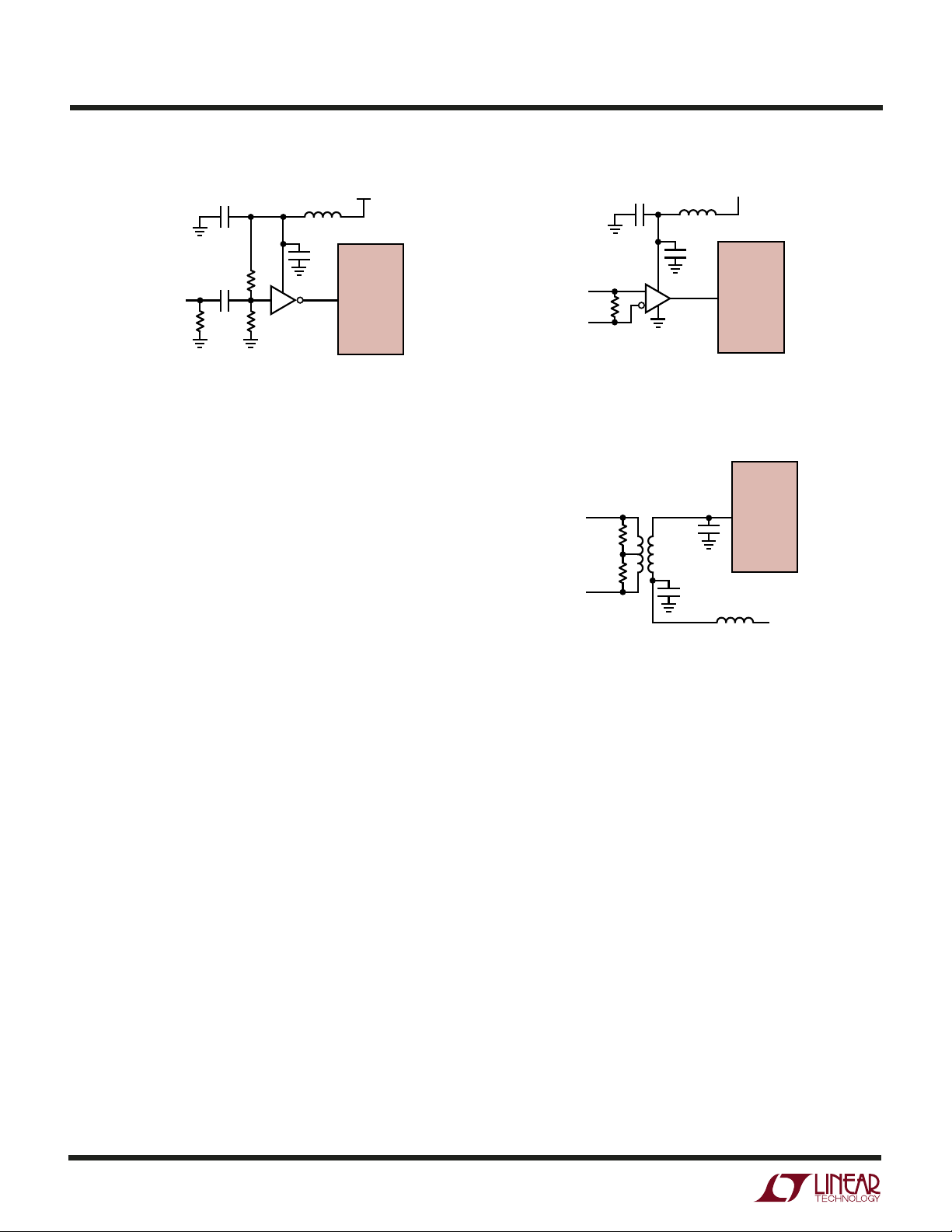
Driving the Clock Input
The CLK inputs can be driven directly with a CMOS or TTL
level signal. A sinusoidal clock can also be used along with
a low jitter squaring circuit before the CLK pin (Figure 11).
228876fa
19
Page 20
LTC2288/LTC2287/LTC2286
WUUU
APPLICATIO S I FOR ATIO
CLEAN
FERRITE
BEAD
0.1µF
CLK
SUPPLY
LTC2288
LTC2287
LTC2286
228876 F11
SINUSOIDAL
CLOCK
INPUT
50Ω
4.7µF
0.1µF
1k
1k
NC7SVU04
Figure 11. Sinusoidal Single-Ended CLK Drive
The noise performance of the LTC2288/LTC2287/LTC2286
can depend on the clock signal quality as much as on the
analog input. Any noise present on the clock signal will
result in additional aperture jitter that will be RMS summed
with the inherent ADC aperture jitter.
In applications where jitter is critical, such as when digitizing high input frequencies, use as large an amplitude as
possible. Also, if the ADC is clocked with a sinusoidal
signal, filter the CLK signal to reduce wideband noise and
distortion products generated by the source.
It is recommended that CLKA and CLKB are shorted
together and driven by the same clock source. If a small
time delay is desired between when the two channels
sample the analog inputs, CLKA and CLKB can be driven
by two different signals. If this delay exceeds 1ns, the
performance of the part may degrade. CLKA and CLKB
should not be driven by asynchronous signals.
Figures 12 and 13 show alternatives for converting a
differential clock to the single-ended CLK input. The use of
a transformer provides no incremental contribution to
phase noise. The LVDS or PECL to CMOS translators
provide little degradation below 70MHz, but at 140MHz
will degrade the SNR compared to the transformer solution. The nature of the received signals also has a large
bearing on how much SNR degradation will be experienced. For high crest factor signals such as WCDMA or
OFDM, where the nominal power level must be at least 6dB
to 8dB below full scale, the use of these translators will
have a lesser impact.
The transformer shown in the example may be terminated
with the appropriate termination for the signaling in use.
CLEAN
FERRITE
BEAD
0.1µF
CLK
SUPPLY
LTC2288
LTC2287
LTC2286
228876 F12
4.7µF
100Ω
IF LVDS USE FIN1002 OR FIN1018.
FOR PECL, USE AZ1000ELT21 OR SIMILAR
Figure 12. CLK Drive Using an LVDS or PECL to CMOS Converter
DIFFERENTIAL
CLOCK
INPUT
ETC1-1T
5pF-30pF
0.1µF
CLK
FERRITE
BEAD
LTC2288
LTC2287
LTC2286
228876 F13
V
CM
Figure 13. LVDS or PECL CLK Drive Using a Transformer
The use of a transformer with a 1:4 impedance ratio may
be desirable in cases where lower voltage differential
signals are considered. The center tap may be bypassed to
ground through a capacitor close to the ADC if the differential signals originate on a different plane. The use of a
capacitor at the input may result in peaking, and depending on transmission line length may require a 10Ω to 20Ω
ohm series resistor to act as both a low pass filter for high
frequency noise that may be induced into the clock line by
neighboring digital signals, as well as a damping mechanism for reflections.
Maximum and Minimum Conversion Rates
The maximum conversion rate for the LTC2288/LTC2287/
LTC2286 is 65Msps (LTC2288), 40Msps (LTC2287), and
25Msps (LTC2286). For the ADC to operate properly, the CLK
signal should have a 50% (±5%) duty cycle. Each half cycle
must have at least 7.3ns (LTC2288), 11.8ns (LTC2287), and
18.9ns (LTC2286) for the ADC internal circuitry to have
enough settling time for proper operation.
20
228876fa
Page 21
WUUU
APPLICATIO S I FOR ATIO
LTC2288/LTC2287/LTC2286
An optional clock duty cycle stabilizer circuit can be used
if the input clock has a non 50% duty cycle. This circuit
uses the rising edge of the CLK pin to sample the analog
input. The falling edge of CLK is ignored and the internal
falling edge is generated by a phase-locked loop. The
input clock duty cycle can vary from 40% to 60% and the
clock duty cycle stabilizer will maintain a constant 50%
internal duty cycle. If the clock is turned off for a long
period of time, the duty cycle stabilizer circuit will require
a hundred clock cycles for the PLL to lock onto the input
clock. To use the clock duty cycle stabilizer, the MODE pin
should be connected to 1/3V
or 2/3VDD using external
DD
resistors. The MODE pin controls both Channel A and
Channel B—the duty cycle stabilizer is either on or off for
both channels.
The lower limit of the LTC2288/LTC2287/LTC2286 sample
rate is determined by droop of the sample-and-hold circuits. The pipelined architecture of this ADC relies on
storing analog signals on small valued capacitors. Junction leakage will discharge the capacitors. The specified
minimum operating frequency for the LTC2288/LTC2287/
LTC2286 is 1Msps.
Digital Output Buffers
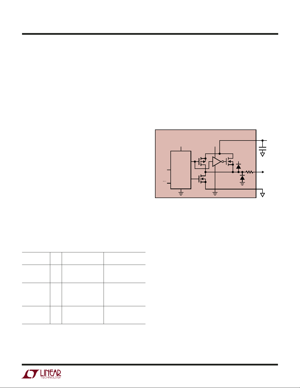
Figure 14 shows an equivalent circuit for a single output
buffer. Each buffer is powered by OV
and OGND, iso-
DD
lated from the ADC power and ground. The additional
N-channel transistor in the output driver allows operation
down to low voltages. The internal resistor in series with
the output makes the output appear as 50Ω to external
circuitry and may eliminate the need for external damping
resistors.
LTC2288/LTC2287/LTC2286
V
DD
DATA
PREDRIVER
FROM
LATCH
LOGIC
OE
Figure 14. Digital Output Buffer
V
DD
OV
DD
43Ω
228876 F14
OV
DD
OGND
0.5V
TO 3.6V
0.1µF
TYPICAL
DATA
OUTPUT
DIGITAL OUTPUTS
Table 1 shows the relationship between the analog input
voltage, the digital data bits, and the overflow bit.
Table 1. Output Codes vs Input Voltage
+
A
(2V Range) OF (Offset Binary) (2’s Complement)
>+1.000000V 1 11 1111 1111 01 1111 1111
+0.998047V 0 11 1111 1111 01 1111 1111
+0.996094V 0 11 1111 1110 01 1111 1110
+0.001953V 0 10 0000 0001 00 0000 0001
0.000000V 0 10 0000 0000 00 0000 0000
–0.001953V 0 01 1111 1111 11 1111 1111
–0.003906V 0 01 1111 1110 11 1111 1110
–0.998047V 0 00 0000 0001 10 0000 0001
–1.000000V 0 00 0000 0000 10 0000 0000
<–1.000000V 1 00 0000 0000 10 0000 0000
–
– A
IN
IN
D9 – D0 D9 – D0
As with all high speed/high resolution converters, the digital output loading can affect the performance. The digital
outputs of the LTC2288/LTC2287/LTC2286 should drive a
minimal capacitive load to avoid possible interaction
between the digital outputs and sensitive input circuitry.
The output should be buffered with a device such as an
ALVCH16373 CMOS latch. For full speed operation the
capacitive load should be kept under 10pF.
Lower OV
voltages will also help reduce interference
DD
from the digital outputs.
228876fa
21
Page 22
LTC2288/LTC2287/LTC2286
U
WUU
APPLICATIO S I FOR ATIO
Data Format
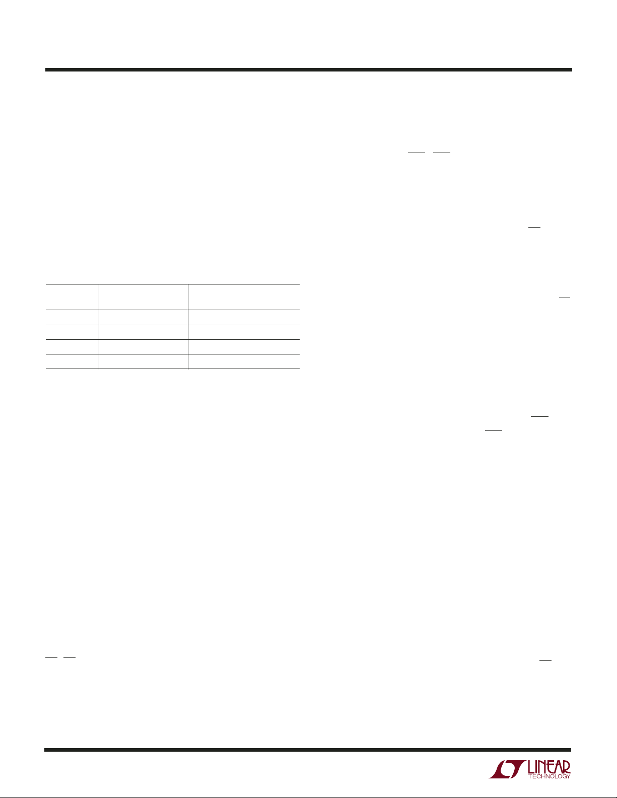
Using the MODE pin, the LTC2288/LTC2287/LTC2286
parallel digital output can be selected for offset binary or
2’s complement format. Note that MODE controls both
Channel A and Channel B. Connecting MODE to GND or
1/3V
MODE to 2/3V
format. An external resistor divider can be used to set the
1/3V
states for the MODE pin.
Table 2. MODE Pin Function
MODE Pin Output Format Cycle Stabilizer
0 Offset Binary Off
1/3V
2/3V
V
Overflow Bit
selects offset binary output format. Connecting
DD
or VDD selects 2’s complement output
DD
or 2/3VDD logic values. Table 2 shows the logic
DD
Clock Duty
DD
DD
DD
Offset Binary On
2’s Complement On
2’s Complement Off
outputs to be enabled and disabled during full speed operation. The output Hi-Z state is intended for use during long
periods of inactivity. Channels A and B have independent
output enable pins (OEA, OEB).
Sleep and Nap Modes
The converter may be placed in shutdown or nap modes
to conserve power. Connecting SHDN to GND results in
normal operation. Connecting SHDN to V
and OE to V
DD
DD
results in sleep mode, which powers down all circuitry
including the reference and typically dissipates 1mW. When
exiting sleep mode it will take milliseconds for the output
data to become valid because the reference capacitors have
to recharge and stabilize. Connecting SHDN to V
and OE
DD
to GND results in nap mode, which typically dissipates
30mW. In nap mode, the on-chip reference circuit is kept
on, so that recovery from nap mode is faster than that from
sleep mode, typically taking 100 clock cycles. In both sleep
and nap modes, all digital outputs are disabled and enter
the Hi-Z state.
When OF outputs a logic high the converter is either
overranged or underranged.
Output Driver Power
Separate output power and ground pins allow the output
drivers to be isolated from the analog circuitry. The power
supply for the digital output buffers, OVDD, should be tied to
the same power supply as for the logic being driven. For
example, if the converter is driving a DSP powered by a 1.8V
supply, then OVDD should be tied to that same 1.8V supply.
OV
can be powered with any voltage from 500mV up to
DD
3.6V. OGND can be powered with any voltage from GND
up to 1V and must be less than OV
swing between OGND and OV
. The logic outputs will
DD
.
DD
Output Enable
The outputs may be disabled with the output enable pin,
OE. OE high disables all data outputs including OF. The data
access and bus relinquish times are too slow to allow the
Channels A and B have independent SHDN pins (SHDNA,
SHDNB). Channel A is controlled by SHDNA and OEA, and
Channel B is controlled by SHDNB and OEB. The nap, sleep
and output enable modes of the two channels are completely
independent, so it is possible to have one channel operating while the other channel is in nap or sleep mode.
Digital Output Multiplexer
The digital outputs of the LTC2288/LTC2287/LTC2286 can
be multiplexed onto a single data bus. The MUX pin is a
digital input that swaps the two data busses. If MUX is High,
Channel A comes out on DA0-DA9, OFA; Channel B comes
out on DB0-DB9, OFB. If MUX is Low, the output busses
are swapped and Channel A comes out on DB0-DB9, OFB;
Channel B comes out on DA0-DA9, OFA. To multiplex both
channels onto a single output bus, connect MUX, CLKA and
CLKB together (see the Timing Diagram for the multiplexed
mode). The multiplexed data is available on either data
bus—the unused data bus can be disabled with its OE pin.
22
228876fa
Page 23

LTC2288/LTC2287/LTC2286
U
WUU
APPLICATIO S I FOR ATIO
Grounding and Bypassing
The LTC2288/LTC2287/LTC2286 requires a printed circuit board with a clean, unbroken ground plane. A multilayer board with an internal ground plane is recommended. Layout for the printed circuit board should ensure that digital and analog signal lines are separated as
much as possible. In particular, care should be taken not
to run any digital track alongside an analog signal track or
underneath the ADC.
High quality ceramic bypass capacitors should be used at
the V
tors must be located as close to the pins as possible. Of
particular importance is the 0.1µF capacitor between
REFH and REFL. This capacitor should be placed as close
to the device as possible (1.5mm or less). A size 0402
ceramic capacitor is recommended. The large 2.2µF ca-
pacitor between REFH and REFL can be somewhat further
away. The traces connecting the pins and bypass capacitors must be kept short and should be made as wide as
possible.
The LTC2288/LTC2287/LTC2286 differential inputs should
run parallel and close to each other. The input traces
should be as short as possible to minimize capacitance
and to minimize noise pickup.
Heat Transfer
Most of the heat generated by the LTC2288/LTC2287/
LTC2286 is transferred from the die through the bottomside exposed pad and package leads onto the printed
circuit board. For good electrical and thermal performance, the exposed pad should be soldered to a large
grounded pad on the PC board. It is critical that all ground
pins are connected to a ground plane of sufficient area.
Clock Sources for Undersampling
Undersampling raises the bar on the clock source and the
higher the input frequency, the greater the sensitivity to
clock jitter or phase noise. A clock source that degrades
SNR of a full-scale signal by 1dB at 70MHz will degrade
SNR by 3dB at 140MHz, and 4.5dB at 190MHz.
In cases where absolute clock frequency accuracy is
relatively unimportant and only a single ADC is required,
, OVDD, VCM, REFH, and REFL pins. Bypass capaci-
DD
a 3V canned oscillator from vendors such as Saronix or
Vectron can be placed close to the ADC and simply
connected directly to the ADC. If there is any distance to
the ADC, some source termination to reduce ringing that
may occur even over a fraction of an inch is advisable. You
must not allow the clock to overshoot the supplies or
performance will suffer. Do not filter the clock signal with
a narrow band filter unless you have a sinusoidal clock
source, as the rise and fall time artifacts present in typical
digital clock signals will be translated into phase noise.
The lowest phase noise oscillators have single-ended
sinusoidal outputs, and for these devices the use of a filter
close to the ADC may be beneficial. This filter should be
close to the ADC to both reduce roundtrip reflection times,
as well as reduce the susceptibility of the traces between
the filter and the ADC. If you are sensitive to close-in phase
noise, the power supply for oscillators and any buffers
must be very stable, or propagation delay variation with
supply will translate into phase noise. Even though these
clock sources may be regarded as digital devices, do not
operate them on a digital supply. If your clock is also used
to drive digital devices such as an FPGA, you should locate
the oscillator, and any clock fan-out devices close to the
ADC, and give the routing to the ADC precedence. The
clock signals to the FPGA should have series termination
at the source to prevent high frequency noise from the
FPGA disturbing the substrate of the clock fan-out device.
If you use an FPGA as a programmable divider, you must
re-time the signal using the original oscillator, and the retiming flip-flop as well as the oscillator should be close to
the ADC, and powered with a very quiet supply.
For cases where there are multiple ADCs, or where the
clock source originates some distance away, differential
clock distribution is advisable. This is advisable both from
the perspective of EMI, but also to avoid receiving noise
from digital sources both radiated, as well as propagated
in the waveguides that exist between the layers of multilayer PCBs.
The differential pairs must be close together, and distanced from other signals. The differential pair should be
guarded on both sides with copper distanced at least 3x
the distance between the traces, and grounded with vias
no more than 1/4 inch apart.
228876fa
23
Page 24
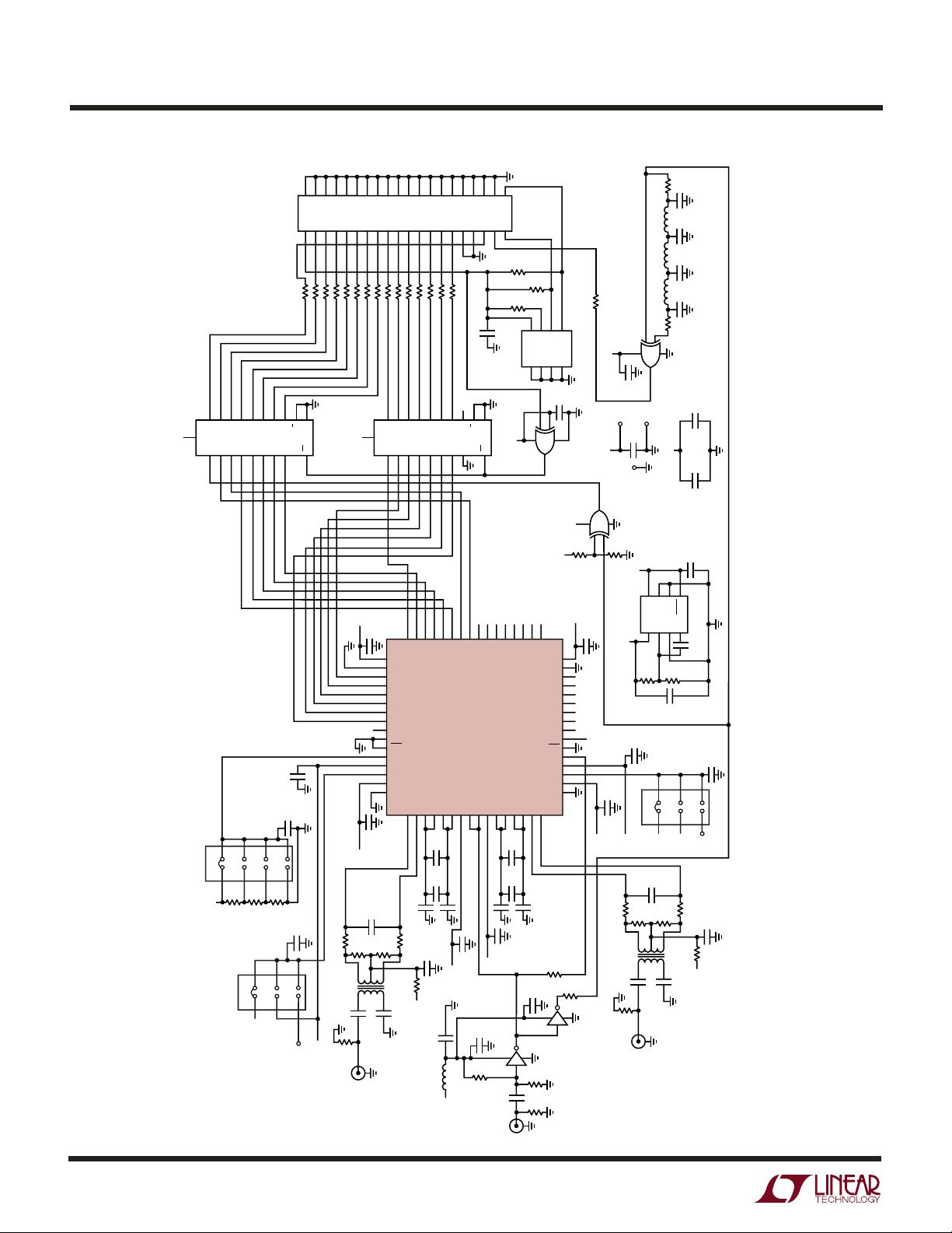
LTC2288/LTC2287/LTC2286
C21
0.1µF
C27
0.1µF
V
DD
V
DD
V
DD
V
DD
V
DD
V
CC
V
CMB
C20
2.2µF
C18 1µF
C23 1µF
C34
0.1µF
C31
12pF
C17
0.1µF
C14
0.1µF
C25
0.1µF
C30
18pF
L2
47nH
R28
24
Ω
C32
18pF
C28
2.2µF
C35
0.1µF
C24
0.1µF
C36
4.7µF
E3
V
DD
3V
E5
PWR
GND
V
DD
V
CC
V
CC
228876 AI01
C1
0.1µF
R16
33Ω
R1
1k
R2
1k
R3
1k
R10
1k
R14
49.9Ω
R20
24.9Ω
R18
24.9Ω
R24
24.9Ω
R17
OPT
R22
24.9Ω
R23
51
T2
ETC1-1T
C29
0.1µF
C33
0.1µF
J3
CLOCK
INPUT
U6
NC7SVU04
U4
NC7SV86P5X
U7
NC7SV86P5X
U3
NC7SVU04
C13
0.1µF
C15
0.1µF
C12
4.7µF
6.3V
L1
BEAD
V
DD
C19
0.1µF
C11
0.1µF
C4
0.1µF
C2
2.2µF
C10
2.2µF
C9 1µF
C13 1µF
R15
1k
J4
ANALOG
INPUT B
V
CC
1
2
3
4
••
5
V
CMB
C8
0.1µF
C6
12pF
C44
0.1µF
R6
24.9Ω
R5
24.9Ω
R9
24.9Ω
R4
OPT
R7
24.9Ω
R8
51
T1
ETC1-1T
C3
0.1µF
C7
0.1µF
J2
ANALOG
INPUT A
1
2
3
5
••
4
V
CMA
V
CMA
12
V
DD
V
DD
34
2/3V
DD
56
1/3V
DD
78
GND
JP1 MODE
C16 0.1µF
25
23
27
29
31
33
35
37
39
21
19
15
17
13
9
7
1
3
5
2
4
11
26
24
30
28
34
32
38
40
39
37
35
33
31
29
27
25
23
21
19
17
15
13
11
9
7
5
3
1
40
3201S-40G1
38
36
34
32
30
28
26
24
22
20
18
16
14
12
10
8
6
4
2
36
22
20
16
18
14
10
8
6
12
R13
10k
R11
10k
R12
10k
R30
15
Ω
R
N1D
33Ω
R
N1C
33Ω
R
N1B
33Ω
R
N1A
33Ω
R
N2D
33Ω
R
N2C
33Ω
R
N2B
33Ω
R
N2A
33Ω
R
N3D
33Ω
R
N3C
33Ω
R
N3B
33Ω
R
N3A
33Ω
R
N4D
33Ω
R
N4C
33Ω
R
N4B
33Ω
C39
1µF
C38
0.01µF
V
CC
V
DD
BYP
GND
ADJ
OUT
SHDN
GND
IN
1
2
3
4
8
U8
LT1763
7
6
5
GND
R26
100k
R25
105k
C37
10µF
6.3V
E4
GND
C40
0.1µF
C41
0.1µF
A
INA
+
A
INA
–
REFHA
REFHA
REFLA
REFLA
V
DD
CLKA
CLKB
V
DD
REFLB
REFLB
REFHB
REFHB
A
INB
–
A
INB
+
1
2
3
4
5
6
7
8
9
10
11
12
13
14
15
16
48
47
46
45
44
43
42
41
40
39
38
37
36
35
34
33
DA3
DA2
DA1
DA0
NC
NC
NC
NC
OFB
DB9
DB8
DB7
DB6
DB5
DB4
DB3
64
63
62
61
60
59
58
57
56
55
54
53
52
51
50
49
GND
V
DD
SENSEA
VCMA
MODE
SHDNA
OEA
OFA
DA9
DA8
DA7
DA6
DA5
DA4
OGND
OV
DD
GND
V
DD
SENSEB
VCMB
MUX
SHDNB
OEB
NC
NC
NC
NC
DB0
DB1
DB2
OGND
OV
DD
17
18
19
20
21
22
23
24
25
26
27
28
29
30
31
32
E2
EXT
REF B
12
V
DD
34
V
CM
V
DD
V
CMB
56
EXT REF
JP3 SENSE
E1
EXT
REF A
12
V
DD
34
V
CM
V
DD
56
EXT REF
JP2 SENSE A
C5
0.1µF
C26
0.1µF
V
CC
B3
B2
B4
B5
B6
B7
OE
B1
B0
A3
A1
A0
18
17
16
15
14
13
12
11
19
2
20
V
CC
74VCX245BQX
V
CC
3
4
5
6
7
8
9
1
10
A2
A7
T/R
GND
A5
A4
A6
B3
B2
B4
B5
B6
B7
OE
B1
B0
A3
A1
A0
18
17
16
15
14
13
12
11
19
2
20
V
CC
74VCX245BQX
V
CC
3
4
5
6
7
8
9
1
10
A2
A7
T/R
GND
A5
A4
A6
A0
A1
A2
A3
V
CC
WP
SCL
SDA
1
2
3
4
8
7
6
5
R29
51
Ω
L4
47nH
C43
8.2pF
L3
47nH
C42
8.2pF
U5
24LC025
V
CC
R31
TBD
R27
TBD
V
CC
U10
NC7SV86P5X
R32
22Ω
U1
LTC2288
U
WUU
APPLICATIO S I FOR ATIO
24
228876fa
Page 25
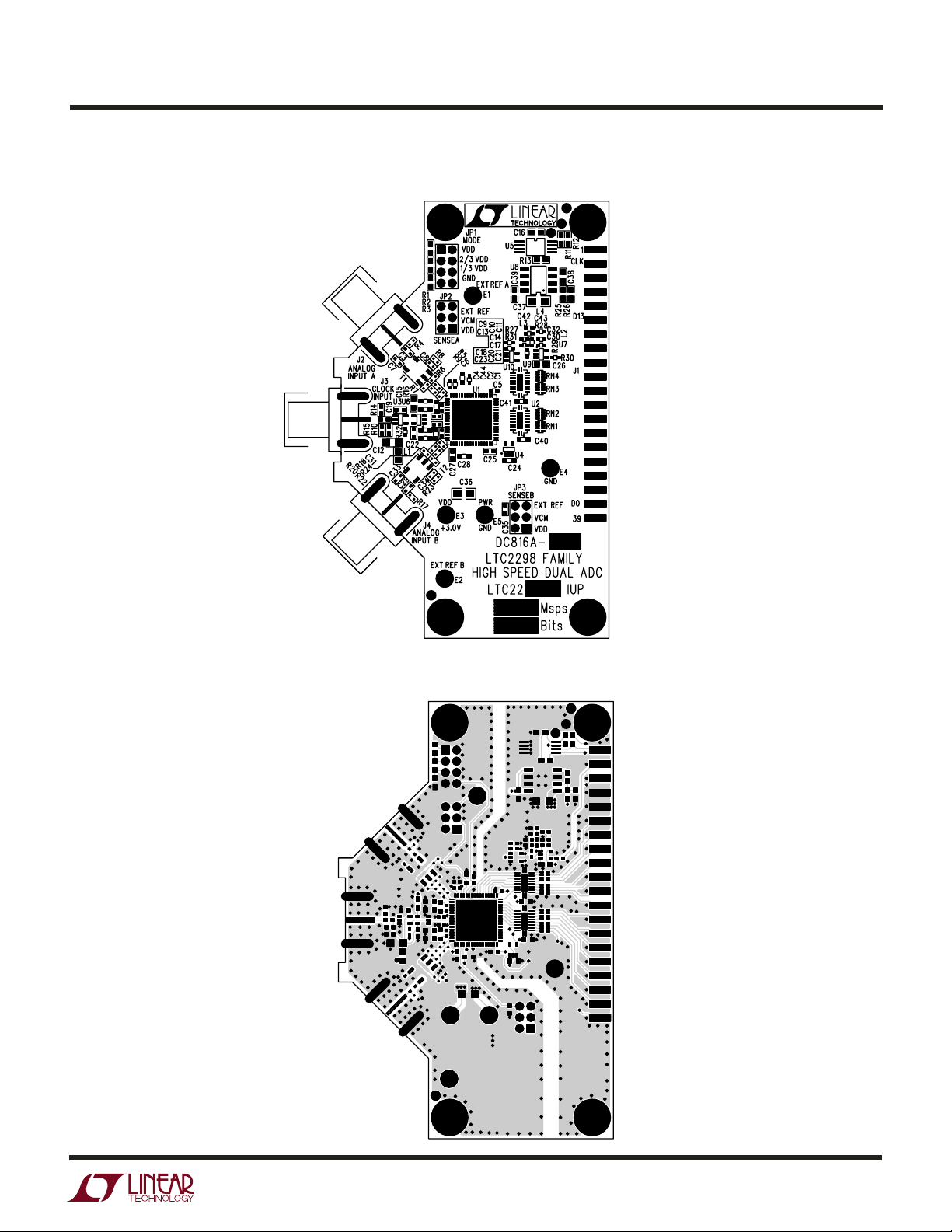
LTC2288/LTC2287/LTC2286
U
WUU
APPLICATIO S I FOR ATIO
Silkscreen Top
Top Side
228876fa
25
Page 26
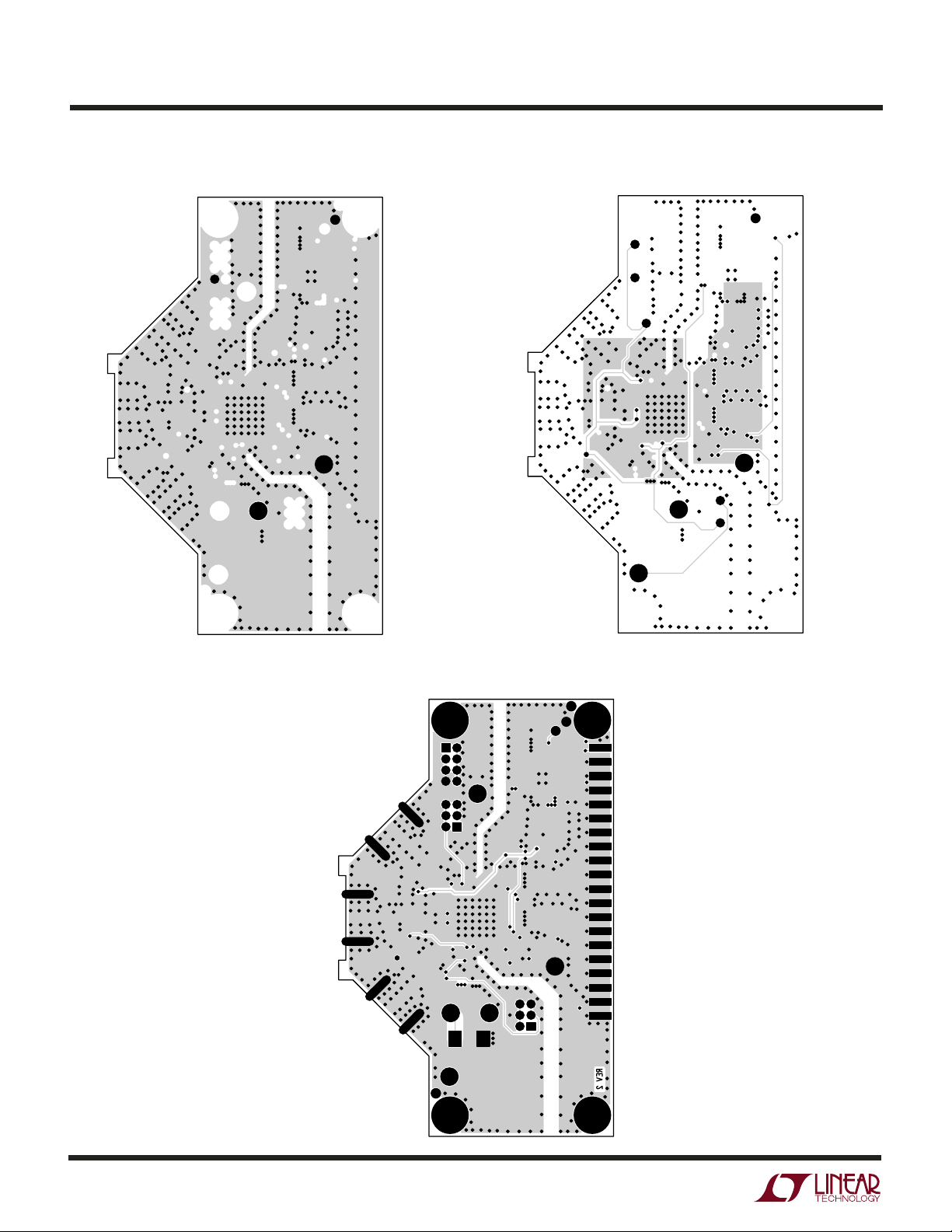
LTC2288/LTC2287/LTC2286
U
WUU
APPLICATIO S I FOR ATIO
Inner Layer 2 GND
Inner Layer 3 Power
Bottom Side
26
228876fa
Page 27
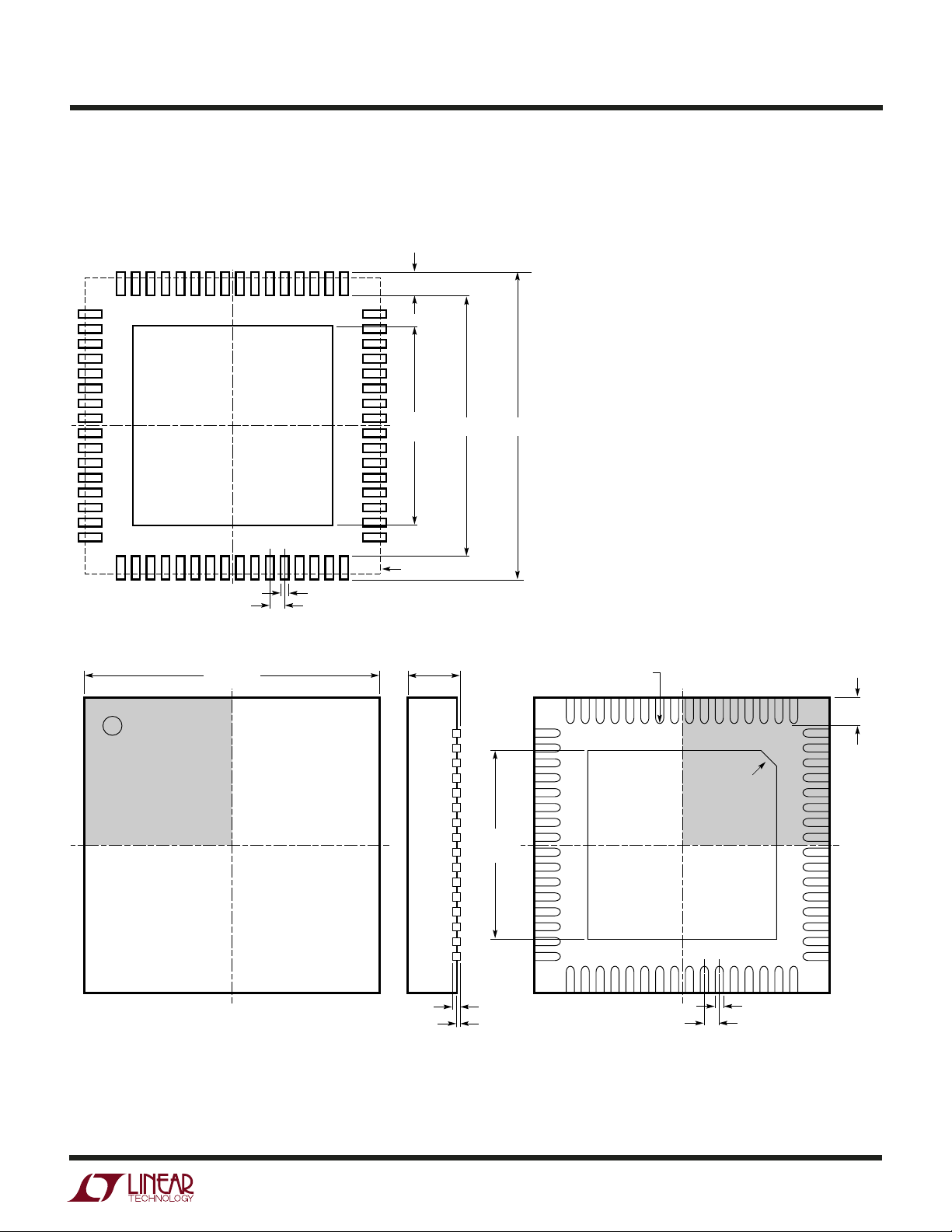
PACKAGE DESCRIPTIO
LTC2288/LTC2287/LTC2286
U
UP Package
64-Lead Plastic QFN (9mm × 9mm)
(Reference LTC DWG # 05-08-1705)
0.70 ±0.05
0.25 ±0.05
0.50 BSC
RECOMMENDED SOLDER PAD PITCH AND DIMENSIONS
9 .00 ± 0.10
(4 SIDES)
PIN 1 TOP MARK
(SEE NOTE 5)
7.15 ±0.05
(4 SIDES)
8.10 ±0.05 9.50 ± 0.05
PACKAGE OUTLINE
0.75 ± 0.05
7.15 ± 0.10
(4-SIDES)
R = 0.115
TYP
PIN 1
CHAMFER
6463
0.40 ± 0.10
1
2
0.200 REF
NOTE:
1. DRAWING CONFORMS TO JEDEC PACKAGE OUTLINE MO-220 VARIATION WNJR-5
2. ALL DIMENSIONS ARE IN MILLIMETERS
3. DIMENSIONS OF EXPOSED PAD ON BOTTOM OF PACKAGE DO NOT INCLUDE
MOLD FLASH. MOLD FLASH, IF PRESENT, SHALL NOT EXCEED 0.20mm ON ANY SIDE, IF PRESENT
4. EXPOSED PAD SHALL BE SOLDER PLATED
5. SHADED AREA IS ONLY A REFERENCE FOR PIN 1 LOCATION ON THE TOP AND BOTTOM OF PACKAGE
6. DRAWING NOT TO SCALE
Information furnished by Linear Technology Corporation is believed to be accurate and reliable.
However, no responsibility is assumed for its use. Linear Technology Corporation makes no representation that the interconnection of its circuits as described herein will not infringe on existing patent rights.
0.00 – 0.05
BOTTOM VIEW—EXPOSED PAD
0.25 ± 0.05
0.50 BSC
(UP64) QFN 1003
228876fa
27
Page 28

LTC2288/LTC2287/LTC2286
RELATED PARTS
PART NUMBER DESCRIPTION COMMENTS
LTC1748 14-Bit, 80Msps 5V ADC 76.3dB SNR, 90dB SFDR, 48-Pin TSSOP Package
LTC1750 14-Bit, 80Msps, 5V Wideband ADC Up to 500MHz IF Undersampling, 90dB SFDR
LT®1993-2 High Speed Differential Op Amp 800MHz BW, 70dBc Distortion at 70MHz, 6dB Gain
LT1994 Low Noise, Low Distortion Fully Differential Input/Output Low Distortion: –94dBc at 1MHz
Amplifier/Driver
LTC2202 16-Bit, 10Msps, 3.3V ADC, Lowest Noise 150mW, 81.6dB SNR, 100dB SFDR, 48-Pin QFN
LTC2208 16-Bit, 130Msps, 3.3V ADC, LVDS Outputs 1250mW, 78dB SNR, 100dB SFDR, 64-Pin QFN
LTC2220-1 12-Bit, 185Msps, 3.3V ADC, LVDS Outputs 910mW, 67.7dB SNR, 80dB SFDR, 64-Pin QFN
LTC2224 12-Bit, 135Msps, 3.3V ADC, High IF Sampling 630mW, 67.6dB SNR, 84dB SFDR, 48-Pin QFN
LTC2255 14-Bit, 125Msps, 3V ADC, Lowest Power 395mW, 72.5dB SNR, 88dB SFDR, 32-Pin QFN
LTC2280 10-Bit, Dual, 105Msps, 3V ADC, Low Crosstalk 320mW, 61.6dB SNR, 85dB SFDR, 64-Pin QFN
LTC2282 12-Bit, Dual, 105Msps, 3V ADC, Low Crosstalk 540mW, 70.1dB SNR, 88dB SFDR, 64-Pin QFN
LTC2284 14-Bit, Dual, 105Msps, 3V ADC, Low Crosstalk 540mW, 72.4dB SNR, 88dB SFDR, 64-Pin QFN
LTC2286 10-Bit, Dual, 25Msps, 3V ADC, Low Crosstalk 150mW, 61.8dB SNR, 85dB SFDR, 64-Pin QFN
LTC2287 10-Bit, Dual, 40Msps, 3V ADC, Low Crosstalk 235mW, 61.8dB SNR, 85dB SFDR, 64-Pin QFN
LTC2288 10-Bit, Dual, 65Msps, 3V ADC, Low Crosstalk 400mW, 61.8dB SNR, 85dB SFDR, 64-Pin QFN
LTC2289 10-Bit, Dual, 80Msps, 3V ADC, Low Crosstalk 422mW, 61.6dB SNR, 85dB SFDR, 64-Pin QFN
LTC2290 12-Bit, Dual, 10Msps, 3V ADC, Low Crosstalk 120mW, 71.3dB SNR, 90dB SFDR, 64-Pin QFN
LTC2291 12-Bit, Dual, 25Msps, 3V ADC, Low Crosstalk 150mW, 71.4dB SNR, 90dB SFDR, 64-Pin QFN
LTC2292 12-Bit, Dual, 40Msps, 3V ADC, Low Crosstalk 235mW, 71.4dB SNR, 90dB SFDR, 64-Pin QFN
LTC2293 12-Bit, Dual, 65Msps, 3V ADC, Low Crosstalk 400mW, 71.3dB SNR, 90dB SFDR, 64-Pin QFN
LTC2294 12-Bit, Dual, 80Msps, 3V ADC, Low Crosstalk 422mW, 70.6dB SNR, 90dB SFDR, 64-Pin QFN
LTC2295 14-Bit, Dual, 10Msps, 3V ADC, Low Crosstalk 120mW, 74.4dB SNR, 90dB SFDR, 64-Pin QFN
LTC2296 14-Bit, Dual, 25Msps, 3V ADC, Low Crosstalk 150mW, 74.5dB SNR, 90dB SFDR, 64-Pin QFN
LTC2297 14-Bit, Dual, 40Msps, 3V ADC, Low Crosstalk 235mW, 74.4dB SNR, 90dB SFDR, 64-Pin QFN
LTC2298 14-Bit, Dual, 65Msps, 3V ADC, Low Crosstalk 400mW, 74.3dB SNR, 90dB SFDR, 64-Pin QFN
LTC2299 14-Bit, Dual, 80Msps, 3V ADC, Low Crosstalk 444mW, 73dB SNR, 90dB SFDR, 64-Pin QFN
LT5512 DC-3GHz High Signal Level Downconverting Mixer DC to 3GHz, 21dBm IIP3, Integrated LO Buffer
LT5514 Ultralow Distortion IF Amplifier/ADC Driver with Digitally 450MHz to 1dB BW, 47dB OIP3, Digital Gain Control 10.5dB to 33dB
Controlled Gain in 1.5dB/Step
LT5515 1.5GHz to 2.5GHz Direct Conversion Quadrature Demodulator High IIP3: 20dBm at 1.9GHz, Integrated LO Quadrature Generator
LT5516 800MHz to 1.5GHz Direct Conversion Quadrature Demodulator High IIP3: 21.5dBm at 900MHz, Integrated LO Quadrature Generator
LT5517 40MHz to 900MHz Direct Conversion Quadrature Demodulator High IIP3: 21dBm at 800MHz, Integrated LO Quadrature Generator
LT5522 600MHz to 2.7GHz High Linearity Downconverting Mixer 4.5V to 5.25V Supply, 25dBm IIP3 at 900MHz. NF = 12.5dB, 50Ω
Single Ended RF and LO Ports
28
Linear Technology Corporation
1630 McCarthy Blvd., Milpitas, CA 95035-7417
(408) 432-1900 ● FAX: (408) 434-0507
●
www.linear.com
228876fa
RD/LT 0106 REV A • PRINTED IN USA
© LINEAR TECHNOLOGY CORPORATION 2005
 Loading...