

Page 1
FEATURES
■
VIN Range: 2.6V to 4.4V
■
Ultralow Power
Operating Current: 14µA
Shutdown Current: <1µA
■
No Inductors
■
Short-Circuit/Thermal Protected
■
Ultrasmall Application Circuit (<0.045in2)
■
Low Profile (1mm) ThinSOT
■
Step-Up Charge Pump Generates 5V
■
Output Current: 10mA
■
VIN to V
■
Switching Frequency: 900kHz
■
Soft-Start Limits Inrush Current at Turn-On
■
Output Driven to Ground During Shutdown
Direct Connection for 3V SIMs
OUT
TM
U
APPLICATIO S
■
GSM Cellular Telephones
■
PCS/DCS Cellular Telephones
■
Portable POS Terminals
LTC1986
3V/5V SIM Power Supply
in ThinSOT
U
DESCRIPTIO
The LTC®1986 is a micropower charge pump DC/DC
converter that provides power for either 3V or 5V GSM
SIM cards. It operates in one of three modes: V
(5V mode), V
= VIN (3V mode) or shutdown. The input
OUT
voltage range is 2.6V to 4.4V and the part can provide
10mA of output current. The LTC1986 allows VIN to drop
as low as 2.6V by providing a boost feature in 3V mode. In
3V mode, V
is connected directly to VIN through a 2.5Ω
OUT
switch until VIN drops below 2.85V. When VIN is below
2.85V, the part automatically boosts V
regulated 2.9V output, thereby ensuring V
to maintain a
OUT
stays within
OUT
the 3V SIM VCC specification.
Extremely low operating current (14µA typical with no
load) and low external parts count make the part ideally
suited for small, light load battery-powered applications.
The total PCB area of the application circuit shown below
is less than 0.045in2. Protection features include inrush
current limiting, undervoltage lockout, short circuit and
thermal overload protection. The LTC1986 is available in
a low profile (1mm) SOT-23 package.
, LTC and LT are registered trademarks of Linear Technology Corporation.
ThinSOT is a trademark of Linear Technology Corporation.
OUT
= 5V
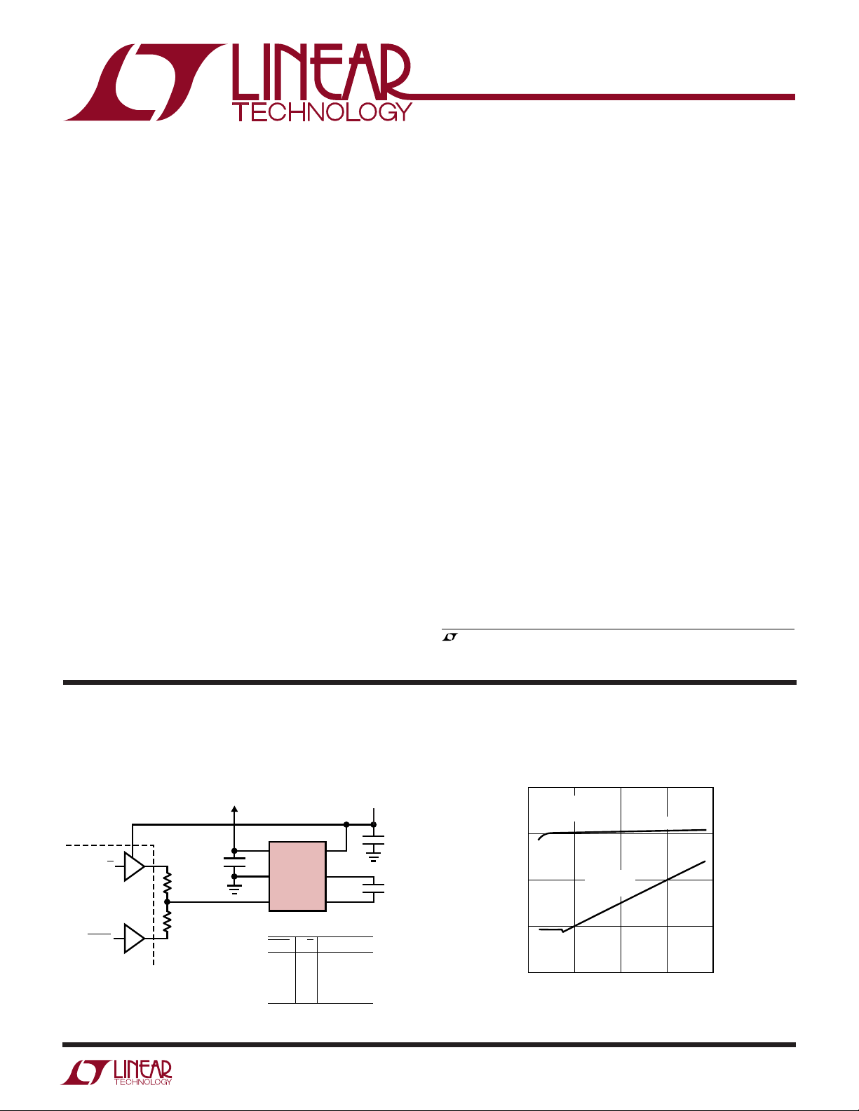
TYPICAL APPLICATIO
3V/5V SIM Power Supply
V
= 5V
OUT
OR V
IN
GSM
CONTROLLER
3/5
SHDN
2.2µF
1M
750k
1
2
3
V
GND
MODE
SHDN
0
0
1
1
U
LTC1986
OUT
3/5
V
IN
+
C1
–
C1
0
SHUTDOWN
1
SHUTDOWN
0
1
V
= 2.6V TO 4.4V
IN
6
5
4
MODE
= 5V
V
OUT
= V
V
OUT
Output Voltage vs Input Voltage
6
TA = 25°C
I
= 10mA
OUT
0.1µF
0.047µF
IN
1986 TA01
5
4
OUTPUT VOLTAGE (V)
3
2
2.5
3.0
3V MODE
(V
OUT
INPUT VOLTAGE (V)
= VIN)
3.5
5V MODE
4.0
4.5
1986 TA02
1986fa
1
Page 2
LTC1986
WW
W
ABSOLUTE MAXIMUM RATINGS
U
U
W
PACKAGE/ORDER INFORMATION
U
(Note 1)
VIN, V
to GND .........................................–0.3V to 6V
OUT
All Other Pins to GND ..................................–0.3V to 6V
V
Short-Circuit Duration............................. Indefinite
OUT
Operating Temperature Range
(Note 2) .................................................. – 40°C to 85°C
Storage Temperature Range ................. –65°C to 150°C
Lead Temperature (Soldering, 10 sec).................. 300°C
TOP VIEW
V
1
OUT
GND 2
MODE 3
S6 PACKAGE
6-LEAD PLASTIC SOT-23
T
= 125°C, θJA = 230°C/ W
JMAX
Consult LTC Marketing for parts specified with wider operating temperature ranges.
6 V
5 C1
4 C1
IN
+
–
ORDER PART
NUMBER
LTC1986ES6
S6 PART MARKING
LTKX
ELECTRICAL CHARACTERISTICS
The ● denotes specifications which apply over the full operating temperature range, otherwise specifications are TA = 25°C.
VIN = V
PARAMETER CONDITIONS MIN TYP MAX UNITS
V
IN
VOUT
V
IN
VIN-to-V
V
OUT
V
OUT
Switching Frequency Oscillator Free-Running 900 kHz
MODE Input Ranges Shutdown Mode
MODE Input Current ● –1 1 µA
Undervoltage Lockout Threshold 1.4 V
Note 1: Absolute Maximum Ratings are those values beyond which the life
of a device may be impaired.
to V
MIN
Operating Voltage ● 2.6 4.4 V
Output Voltage Shutdown Mode 0 V
Operating Current Shutdown Mode, V
ON Resistance 3V Mode, VIN = 3V ● 2.5 5 Ω
OUT
Short-Circuit Current 3V or 5V Mode, V
Discharge Resistance VIN = 3V ● 70 200 Ω
, MODE = VIN, C1 = 0.047µF, C
MAX
= 2.2µF, unless otherwise specified.
OUT
3V Mode. V
3V Mode, V
5V Mode, V
5V Mode, VIN = 2.7V to 4.4V, I
3V Mode, I
5V Mode, I
5V Mode
3V Mode ● V
= 2.85V to 4.4V, I
IN
< 2.85V, I
IN
< 2.7V, I
IN
= 0mA ● 10 25 µA
OUT
= 0mA ● 14 30 µA
OUT
OUT
≤ 10mA ● 4.55 5 5.25 V
OUT
= 0V ● 0.001 1 µA
MODE
= 0V ● 100 200 mA
OUT
Note 2: The LTC1986E is guaranteed to meet performance specifications
from 0°C to 70°C. Specifications over the –40°C to 85°C operating
temperature range are assured by design, characterization and correlation
with statistical process controls.
≤ 10mA V
OUT
< 10mA ● 2.75 2.9 3.05 V
≤ 10mA ● 4.75 5 5.25 V
OUT
● 0V
● V
– 0.025 V
IN
/2 + 0.1 V
IN
– 0.25 V
IN
/2 – 0.1 V
IN
– 1.0 V
IN
IN
V
2
1986fa
Page 3
W
U
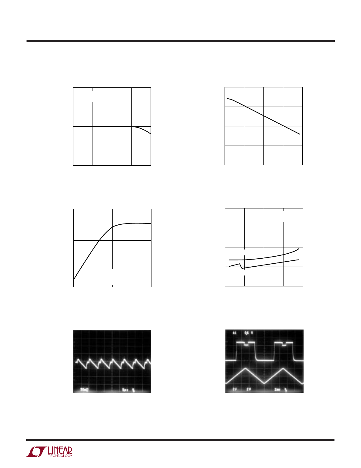
TYPICAL PERFORMANCE CHARACTERISTICS
Output Voltage vs Output Current
(3V Mode)
3.10
3.05
VIN = V
T
A
= 25°C
MODE
= 3V
Efficiency vs Input Voltage
100
80
LTC1986
I
= 10mA
OUT
V
= 5V
OUT
= 25°C
T
A
3.00
OUTPUT VOLTAGE (V)
2.95
2.90
0.001
0.01
OUTPUT CURRENT (mA)
0.1
Efficiency vs Output Current
100
80
60
40
EFFICIENCY (%)
20
0
0.001
VIN = 3V
5V MODE (V
T
= 25°C
A
0.01
OUTPUT CURRENT (mA)
0.1
MODE
1
= 0.6VIN)
1
1986 G03
1986 G01
60
EFFICIENCY (%)
40
20
10
2.5
3.0
3.5
INPUT VOLTAGE (V)
4.0
4.5
1986 G02
Positive Supply Current vs
Input Voltage
40
30
20
5V MODE (V
10
0
3V MODE (V
2.5
POSITIVE SUPPLY CURRENT (mA )
10
MODE
MODE
3.0
INPUT VOLTAGE (V)
= 0.6VIN)
= VIN)
3.5
I
OUT
T
A
= 0mA
= 25°C
4.0
4.5
1986 G04
V
OUT
50mV/DIV
AC COUPLED
Output Voltage Ripple
(5V Mode)
= 3V
V
IN
= 10mA
I
OUT
T
= 25°C 1986 G05
A
5ms/DIV
V
OUT
2V/DIV
V
MODE
2V/DIV
Output Voltage vs
V
Waveforms
MODE
5V
0V
4V
0V
= 4V
V
IN
= 25°C 1986 G06
T
A
2ms/DIV
1986fa
3
Page 4

LTC1986
UUU
PIN FUNCTIONS
V
(Pin 1): Charge Pump Output. The V
OUT
depend on the MODE pin input voltage. V
shutdown mode, V
= VIN in 3V mode and V
OUT
5V mode. The LTC1986 provides a 2.9V regulated output
when the part is in 3V mode and the VIN voltage is below
2.85V. This feature allows the input voltage to be below the
minimum voltage specification for 3V SIM cards without
violating the SIM VCC specification. Bypass the V
with a ≥ 2.2µF low ESR capacitor to ground.
GND (Pin 2): Ground. Connect to a ground plane for best
performance.
MODE (Pin 3): MODE Input Pin. The voltage on this pin
determines the operating mode of the LTC1986. It operates in either shutdown mode, 3V mode or 5V mode
depending on the MODE pin voltage with respect to VIN.
voltage will
OUT
= 0V in
OUT
OUT
= 5V in
pin
OUT
The three different modes can be realized by using two
external resistors as shown in the typical application
circuit. If V
mode.If VIN/2 + 0.1V < V
mode. If VIN – 0.25V < V
< VIN/2 – 0.1V, the part is in shutdown
MODE
< VIN – 1V, the part is in 5V
MODE
, the part is in 3V mode. To
MODE
achieve the lowest possible shutdown current, the MODE
pin should be pulled to 0V, i.e., both the SHDN and 3/5
signals from the controller should be pulled low.
C1– (Pin 4): Charge Pump Flying Capacitor Negative
Terminal.
C1+ (Pin 5): Charge Pump Flying Capacitor Positive
Terminal.
VIN (Pin 6): Input Supply Voltage. Bypass VIN with a
≥ 0.1µF low ESR capacitor to ground.
SI PLIFIEDWBLOCK DIAGRA
50Ω
6
V
MODE
IN
SOFT START
–
1.25V
VIN – 0.6V
3
V
+
+
–
+
–
/2
IN
5V MODE
LOGIC
W
2.9V BOOST
900kHz
OSC
3V
5V
SHDN
–
C1
45
CHARGE
PUMP
UVLO/
THERMAL
SHDN
+
C1
LTC1986
2.5Ω
1.25V
REF
3V MODE
+
–
SHDN
V
1
OUT
4
GND
2
1986 BD
1986fa
Page 5

LTC1986
U
WUU
APPLICATIONS INFORMATION
Operation
The LTC1986 is a charge pump DC/DC converter designed
specifically to supply VCC power for either 3V or 5V SIM
cards. The part can operate in one of three modes: a low
power shutdown mode which disconnects VIN from V
and actively pulls down the V
supply, 3V mode which
OUT
provides a direct connection between VIN and V
powering 3V SIM cards, and 5V mode which provides a
regulated 5V output for powering 5V SIM cards. In 5V
mode, regulation is achieved by sensing the output voltage through a resistor divider and enabling the charge
pump as needed to maintain regulation.
When the charge pump is enabled, a 2-phase
nonoverlapping clock controls the internal charge pump
switches. Flying capacitor C1 is charged to VIN on phase
one of the clock. On phase two of the clock, C1 is stacked
in series with VIN and connected to V
through an
OUT
internal switch. This sequence of charging and discharging the flying capacitor occurs at a free-running frequency
of 900kHz (typ) and continues until the divided output
voltage reaches the upper trip point of the comparator.
Once the output is in regulation, the charge pump is
disabled. This method of bursting the charge pump on and
off enables the LTC1986 to achieve high efficiency at
extremely low output loads.
Mode Selection
OUT
OUT
for
The three modes can be selected using two totem pole
digital outputs and two external resistors as shown in
Figure 1.
Shutdown mode disconnects VIN from V
an internal pull-down device which forces V
and enables
OUT
to GND.
OUT
To achieve the lowest possible quiescent current in shutdown mode, the voltage on the MODE pin should be pulled
below 0.4V. 3V mode connects V
to VIN through a 2.5Ω
OUT
internal switch. The LTC1986 has the additional capability
of boosting V
to a regulated 2.9V in 3V mode when the
OUT
input voltage drops below 2.85V. This ensures that the 3V
SIM VCC specification is not violated if VIN drops below
2.7V during transients or low battery conditions.
V
IN
6
V
IN
LTC1986
MODE
SHUTDOWN (I
SHUTDOWN (I
V
OUT
V
OUT
MODE
= 5V
= V
< 1µA)
CC
= 10µA)
CC
IN
1986 F01
SHDN
3/5
1M
750k
SHDN
0
0
1
1
3
3/5
0
1
0
1
Figure 1
The operating mode is determined by the voltage applied
to the MODE pin. The MODE pin has three voltage thresholds—all of which are referenced to VIN:
Shutdown Mode ⇒V
5V Mode ⇒VIN/2 + 0.1V < V
3V Mode ⇒VIN – 0.25V < V
< VIN/2 – 0.1V
MODE
MODE
MODE
< VIN – 1V
For example, if VIN = 3V, then the following table applies:
V
MODE
0V to 1.4V Shutdown Mode
1.6V to 2V 5V Mode
2.75V to 3V 3V Mode (V
OPERATING MODE
= VIN)
OUT
Capacitor Selection
For best performance, it is recommended that low ESR
capacitors be used for both CIN and C
and ripple. The CIN and C
capacitors should be either
OUT
to reduce noise
OUT
ceramic or tantalum. Ceramic capacitors will provide the
smallest size for a given capacitance. If the input source
impedance is very low (<0.5Ω), CIN may not be needed.
For best performance, C
should be 2.2µF or greater.
OUT
Ceramic capacitors are also recommended for the flying
capacitor C1 with values between 0.047µF and 0.22µF. If
a small value output capacitor (3.3µF or less) is used, a
small flying capacitor should also be used to prevent high
output ripple in 5V mode. The recommended capacitor
values to minimize board space and cost are: CIN = 0.1µF,
C1 = 0.047µF and C
= 2.2µF (ceramic).
OUT
1986fa
5
Page 6

LTC1986
U
WUU
APPLICATIONS INFORMATION
Output Ripple
Normal 5V mode operation produces voltage ripple on the
V
pin. Output voltage ripple is required for regulation.
OUT
Low frequency ripple exists due to the hysteresis in the
sense comparator and propagation delays in the charge
pump enable/disable circuits. High frequency ripple is
also present mainly from the ESR (equivalent series resistance) in the output capacitor. Typical output ripple with
VIN = 3V under maximum load is 75mV
2.2µF output capacitor and a 0.047µF C1 capacitor. For
applications requiring VIN to exceed 3.3V or for applications requiring <75mV of peak-to-peak ripple, a 3.3µF to
10µF C
creases in output ripple can be achieved by using C
capacitors larger than 10µF.
capacitor is recommended. Slight further de-
OUT
with a low ESR
P-P
OUT
Protection Features
The LTC1986 provides several protection features.
Undervoltage lockout prevents any current from flowing
between VIN and V
exceeds 1.4V (typ). This prevents undesirable glitches
during power-up. The parts also limit inrush current
during power-up to under 200mA regardless of VIN voltage, operating mode and output load by disabling the main
direct connect switch (3V mode) or the charge pump
(5V mode) and enabling a 50Ω series switch between V
and V
short-circuit protected and can survive an indefinite short
from V
voltage. In the event of thermal overload, the parts will
enter thermal shutdown if the junction temperature
exceeds 165°C and return to normal operation once the
junction temperature drops to 150°C.
until V
OUT
to GND regardless of operating mode or input
OUT
reaches VIN/2. The parts are also
OUT
until the VIN voltage
OUT
IN
6
1986fa
Page 7

PACKAGE DESCRIPTION
LTC1986
U
S6 Package
6-Lead Plastic TSOT-23
(Reference LTC DWG # 05-08-1636)
0.62
MAX
3.85 MAX
2.62 REF
RECOMMENDED SOLDER PAD LAYOUT
PER IPC CALCULATOR
0.20 BSC
DATUM ‘A’
NOTE:
1. DIMENSIONS ARE IN MILLIMETERS
2. DRAWING NOT TO SCALE
3. DIMENSIONS ARE INCLUSIVE OF PLATING
4. DIMENSIONS ARE EXCLUSIVE OF MOLD FLASH AND METAL BURR
5. MOLD FLASH SHALL NOT EXCEED 0.254mm
6. JEDEC PACKAGE REFERENCE IS MO-193
0.95
REF
1.22 REF
1.4 MIN
0.30 – 0.50 REF
2.80 BSC
0.09 – 0.20
(NOTE 3)
1.50 – 1.75
(NOTE 4)
1.00 MAX
0.95 BSC
0.80 – 0.90
2.90 BSC
(NOTE 4)
PIN ONE ID
1.90 BSC
0.30 – 0.45
6 PLCS (NOTE 3)
0.01 – 0.10
S6 TSOT-23 0302
Information furnished by Linear Technology Corporation is believed to be accurate and reliable.
However, no responsibility is assumed for its use. Linear Technology Corporation makes no representation that the interconnection of its circuits as described herein will not infringe on existing patent rights.
1986fa
7
Page 8

LTC1986
TYPICAL APPLICATION
U
3V/5V SIM Power Supply
V
= 5V
OUT
OR V
IN
V
= 2.6V TO 4.4V
IN
GSM
CONTROLLER
3/5
SHDN
2.2µF
1M
750k
1
2
3
LTC1986
V
OUT
GND
MODE
SHDN
0
0
1
1
V
C1
C1
3/5
0
1
0
1
6
IN
5
+
4
–
MODE
SHUTDOWN
SHUTDOWN
V
OUT
= V
V
OUT
= 5V
0.1µF
0.047µF
IN
1986 TA01
RELATED PARTS
PART NUMBER DESCRIPTION COMMENTS
LTC1503 High Efficiency Step-Down Charge Pump VIN = 2.4V to 6V, 100mA Output Current
LTC1517 Micropower Charge Pump in 5-Pin ThinSOT
LTC1555 SIM Power Supply and Level Translator VIN = 2.7V to 10V, 10kV ESD on SIM Contact Pins
LT1615 Micropower Step-Up DC/DC Converter in ThinSOT VIN = 1.2V to 15V; 350mA, 36V Switch
LT1682 Charge Pump Plus Low Noise LDO Regulator in MS8 50mA Output Current; 60µV
LTC1754-5 5V Charge Pump with Shutdown in ThinSOT 50mA Output Current, ICC = 13µA
LTC1754-3.3 3.3V Charge Pump with Shutdown in ThinSOT VIN = 2V to 4.4V; I
LT1761 Low Noise, 100mA Micropower LDO Regulator IQ = 20µA, 20µV
LTC1755 Smart Card Power Supply and Level Translator ISO 7816-3 and EMV Compliant
LTC1911-1.5/LTC1911-1.8 High Efficiency, Inductorless, Low Noise Step-Down Up to 85% Efficiency, 1.5MHz, VIN: 2.7V to 5.5V,
DC/DC Converter I
LTC3250-1.5 High Efficiency, Inductorless, Low Noise Step-Down Up to 90% Efficiency, 1.5MHz, VIN: 3.1V to 5.5V,
DC/DC Converter I
TM
ICC = 6µA, Short-Circuit/Thermal Protected
Output Noise
RMS
= 40mA; Ripple = 23mV
OUT
Noise, ThinSOT
RMS
= 180µA, MS8
Q
= 35µA, ThinSOT
Q
P-P
8
Linear Technology Corporation
1630 McCarthy Blvd., Milpitas, CA 95035-7417
(408) 432-1900 ● FAX: (408) 434-0507
●
www.linear.com
1986fa
LT/TP 0902 1K REV A • PRINTED IN USA
LINEAR TECHNOLOGY CORPORATION 1999
Page 9

 Loading...