Linear LTC1588CG, LTC1588IG, LTC1589CG, LTC1589IG, LTC1592ACG Schematics
...
with Programmable Output Range
FEATURES
■
Six Programmable Output Ranges
Unipolar Mode: 0V to 5V, 0V to 10V
Bipolar Mode: ±5V, ±10V, ±2.5V, –2.5V to 7.5V
■
1LSB Max DNL and INL Over the Industrial
Temperature Range
■
Glitch Impulse < 2nV-s
■
16-Lead SSOP Package
■
Power-On Reset to 0V
■
Asynchronous Clear to 0V for All Ranges
U
APPLICATIO S
■
Process Control and Industrial Automation
■
Precision Instrumentation
■
Direct Digital Waveform Generation
■
Software-Controlled Gain Adjustment
■
Automatic Test Equipment
LTC1588/LTC1589/LTC1592
12-/14-/16-Bit SoftSpan DACs
U
DESCRIPTIO
The LTC®1588/LTC1589/LTC1592 are serial input 12-/14/16-bit multiplying current output DACs that operates
from a single 5V supply. These SoftSpanTM DACs can be
software-programmed for either unipolar or bipolar mode
through a 3-wire SPI interface. In either mode, the voltage
output range can also be software-programmed. Two
output ranges in unipolar mode and four output ranges in
bipolar mode are available.
INL and DNL are accurate to 1LSB over the industrial
temperature range in both unipolar and bipolar modes.
True 16-bit 4-quadrant multiplication is achieved with
on-chip four quadrant multiplication resistors. The
LTC1588/LTC1589/LTC1592 are available in a 16-lead
SSOP package.
These devices include an internal deglitcher circuit that
reduces the glitch impulse to less than 2nV-s (typ).
The asynchronous clear pin resets the LTC1588/LTC1589/
LTC1592 to 0V in unipolar or bipolar mode.
, LTC and LT are registered trademarks of Linear Technology Corporation.
SoftSpan is a trademark of Linear Technology Corporation.
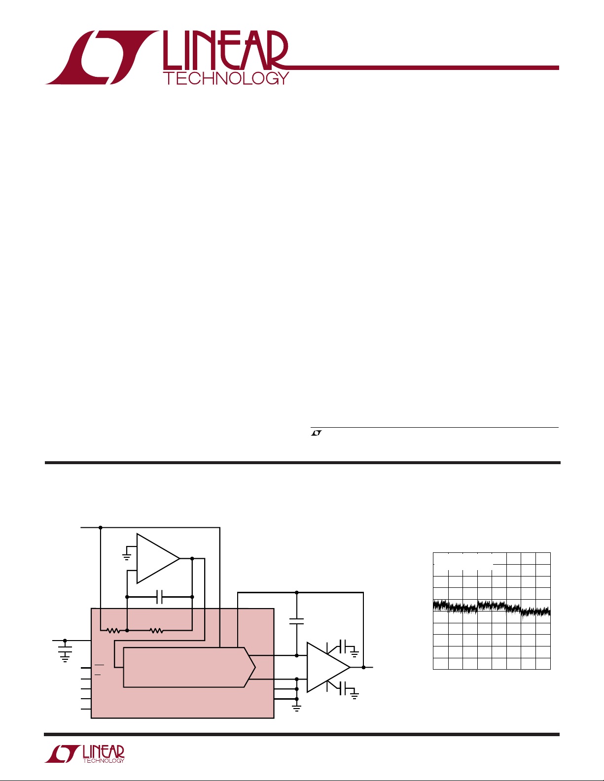
TYPICAL APPLICATIO
Programmable Output Range 16-Bit SoftSpan DAC
V
REF
5V
5
+
1/2 LT®1469
6
–
1
2
R
R1
9
5V
0.1µF
V
CC
14
CLR
13
CS/LD
12
SCK
11
SDI
10
SDO
COM
R1
16-BIT DAC WITH SPAN ADJUST
C2
150pF
R2
7
LTC1592
U
LTC1592 Integral Nonlinearity
1.0
V
= 5V
REF
0.8
ALL OUTPUT RANGES
0.6
0.4
3
15
16
R2
REF
4
R
R
FB
OFS
I
OUT1
I
OUT2
AGND
GND
1588992 TA01
C1
15pF
5
2
3
6
7
8
15V
8
–
1/2 LT1469
+
4
–15V
0.1µF
0.1µF
1
V
OUT
0.2
0
–0.2
–0.4
–0.6
INTEGRAL NONLINEARITY (LSB)
–0.8
–1.0
0
32768
16384
DIGITAL INPUT CODE
49152
65535
1588992 TA02
1588992fa
1
LTC1588/LTC1589/LTC1592
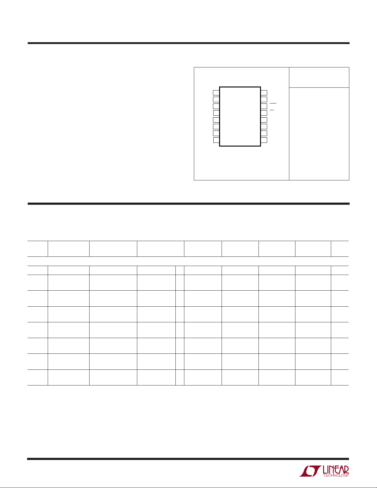
PACKAGE/ORDER I FOR ATIO
UU
W
WWWU
ABSOLUTE AXI U RATI GS
(Note 1)
VCC to AGND, GND ......................................–0.3V to 7V
AGND to GND .............................. –0.3V to (VCC + 0.3V)
GND to AGND .............................. –0.3V to (VCC + 0.3V)
R
to AGND, GND ................................ –0.3V to 12V
COM
REF to AGND, GND ................................................ ±15V
R
, RFB, R1, R2 to AGND, GND .......................... ±15V
OFS
Digital Inputs to AGND, GND ....... –0.3V to (VCC + 0.3V)
I
, I
OUT1
Maximum Junction Temperature .......................... 150°C
Operating Temperature Range
LTC1588C/LTC1589C/LTC1592C ........... 0°C to 70°C
LTC1588I/LTC1589I/LTC1592I........... –40°C to 85°C
Storage Temperature Range ................. –65°C to 150°C
Lead Temperature (Soldering, 10 sec).................. 300°C
to AGND, GND.......... –0.3V to (VCC + 0.3V)
OUT2
ORDER PART
TOP VIEW
1
R
COM
2
R1
3
R
OFS
4
R
FB
5
I
OUT1
6
I
OUT2
7
AGND
8
GND
G PACKAGE
16-LEAD PLASTIC SSOP
T
= 150°C, θJA = 125°C/ W
JMAX
Consult LTC Marketing for parts specified with wider operating temperature ranges.
16
R2
15
REF
14
CLR
13
CS/LD
12
SCK
11
SDI
10
SDO
9
V
CC
NUMBER
LTC1588CG
LTC1588IG
LTC1589CG
LTC1589IG
LTC1592ACG
LTC1592AIG
LTC1592BCG
LTC1592BIG
ELECTRICAL CHARACTERISTICS
The ● denotes specifications which apply over the full operating temperature range, otherwise specifications are TA = T
VCC = 5V, V
SYMBOL PARAMETER CONDITIONS TEMPERATURE MIN TYP MAX MIN TYP MAX MIN TYP MAX MIN TYP MAX UNITS
Accuracy
INL Integral (Notes 2, 3) TA = 25°C ±1 ±1 ±2 ±0.3 ±1LSB
DNL Differential Guaranteed T
GE Gain Error All Output Ranges TA = 25°C –0.20 ±3 –1.0 ±4–3±16 –2 ±16 LSB
BZE Bipolar Zero Error All Bipolar Ranges TA = 25°C ±1 ±2.5 ±10 ±5LSB
I
LKG
PSRR Power Supply VCC = 5V ±10% ● ±0.01±0.15 ±0.05 ±0.5 ±2 ±0.2 ±2 LSB/V
= 5V, I
REF
Resolution ● 12 14 16 16 Bits
Nonlinearity T
Nonlinearity Monotonic (Note 3)
Gain Temperature ∆Gain/∆Temperature ● 3 3 3 1 3 ppm/°C
Coefficient (Note 4)
I
Leakage (Note 5) TA = 25°C ±5 ±5 ±5 ±5nA
OUT1
Current T
Rejection
= AGND = GND = 0V.
OUT2
(Note 3) T
(Note 3) T
MIN
MIN
MIN
MIN
MIN
to T
to T
to T
to T
to T
MAX
MAX
MAX
MAX
MAX
LTC1588 LTC1589 LTC1592B LTC1592A
● ±1 ±1 ±2 ±0.4 ±1LSB
● ±1 ±1 ±1 ±0.2 ±1LSB
● –0.22 ±3 –1.3 ±6–4±24 –3 ±16 LSB
● ±1 ±4.0 ±16 ±8LSB
● ±15 ±15 ±15 ±15 nA
MIN
to T
MAX
,
2
1588992fa
LTC1588/LTC1589/LTC1592
ELECTRICAL CHARACTERISTICS
temperature range, otherwise specifications are TA = T
The ● denotes specifications which apply over the full operating
MIN
to T
, VCC = 5V, V
MAX
REF
= 5V, I
= AGND = GND = 0V.
OUT2
SYMBOL PARAMETER CONDITIONS MIN TYP MAX UNITS
Reference Input
R
REF
DAC Input Resistance (Unipolar) (Note 6) ● 5710 kΩ
R1, R2 R1, R2 Resistance (Notes 6, 11) ● 10 14 20 kΩ
R
OFS
R
FB
Offset Resistance (Bipolar) ±5V, ±10V, ±2.5V Ranges ● 10 14 20 kΩ
–2.5V to 7.5V Range
● 20 28 40 kΩ
Feedback Resistance (Unipolar) 5V Range ● 5710 kΩ
10V Range
● 10 14 20 kΩ
Feedback Resistance (Bipolar) ±5V and –2.5V to 7.5V Ranges ● 10 14 20 kΩ
±10V Range
±2.5V Range
● 20 28 40 kΩ
● 5710 kΩ
Analog Outputs (Note 4)
C
OUT
Output Capacitance (I
) DAC Load All 1s 160 pF
OUT1
DAC Load All 0s 100 pF
AC Performance (Note 4)
Settling Time 5V Range, 0V to 5V Step with LT1468 (Note 7) 2 µs
Midscale Glitch Impulse (Note 10) 2 nV-s
Multiplying Feedthrough Error V
= ±10V, 10kHz Sine Wave 1 mV
REF
P-P
THD Total Harmonic Distortion (Note 8) Multiplying –108 dB
Output Noise Voltage Density (Note 9) At I
OUT1
11 nV/√Hz
Digital Inputs
V
IH
V
IL
I
IN
C
IN
Digital Input High Voltage ● 2.4 V
Digital Input Low Voltage ● 0.8 V
Digital Input Current ● ±1 µA
Digital Input Capacitance VIN = 0V (Note 4) ● 8pF
Digital Outputs
V
OH
V
OL
Digital Output High Voltage IOH = 200µA ● 4V
Digital Output Low Voltage IOL = 1.6mA ● 0.4 V
Timing Characteristics
t
1
t
2
t
3
t
4
t
5
t
6
t
7
t
8
t
9
t
10
t
11
Serial Input Valid to SCK Setup Time ● 60 ns
Serial Input Valid to SCK Hold Time ● 0ns
SCK Pulse Width High ● 35 ns
SCK Pulse Width Low ● 35 ns
CS/LD Pulse High Width ● 360 ns
LSB SCK High to CS/LD High ● 35 ns
CS/LD Low to SCK High ● 0ns
SCK to SDO Propagation Delay C
= 50pF ● 20 180 ns
LOAD
SCK Low to CS/LD Low ● 35 ns
Clear Pulse Low Width ● 100 ns
CS/LD High to SCK Positive Edge ● 35 ns
SCK Frequency Non-Daisy Chain (Note 12) ● 14.2 MHz
Daisy Chain (Note 13) 4.1 MHz
1588992fa
3
LTC1588/LTC1589/LTC1592
ELECTRICAL CHARACTERISTICS
temperature range, otherwise specifications are TA = T
The ● denotes specifications which apply over the full operating
MIN
to T
, VCC = 5V, V
MAX
REF
= 5V, I
= AGND = GND = 0V.
OUT2
SYMBOL PARAMETER CONDITIONS MIN TYP MAX UNITS
Power Supply
V
CC
I
CC
Note 1: Absolute Maximum Ratings are those values beyond which the life
of a device may be impaired.
Note 2: ±1LSB = ±0.0015% of full scale = ±15.3ppm of full scale
(LTC1592). ±1LSB = ±0.006% of full scale = ±61.2ppm of full scale
(LTC1589). ±1LSB = 0.024% of full scale = ±244.8ppm of full scale
(LTC1588).
Note 3: Using internal feedback resistor.
Note 4: Guaranteed by design, not subject to test.
Note 5: I
Note 6: Typical temperature coefficient is 100ppm/°C.
Note 7: To 0.0015% for a full-scale change, measured from the falling
edge of LD for the LTC1592 only.
Note 8: REF = 6V
Supply Voltage ● 4.5 5 5.5 V
Supply Current, V
CC
Digital Inputs = 0V or V
CC
● 10 µA
Note 9: Calculation from en = √4kTRB where: k = Boltzmann constant
(1.38E-23 J/°K); R = resistance (Ω); T = temperature (°K); B = bandwidth
(Hz).
Note 10: Midscale transition code: 32767 to 32768 for the LTC1592, 8191
to 8192 for the LTC1589, 2047 to 2048 for the LTC1588.
Note 11: R1 and R2 are measured between R1 and R
, R2 and R
COM
COM
Note 12: If a continuous clock is used with data changing on the rising
, t2) will limit the maximum clock
1
with DAC register loaded to all 0s.
OUT1
edge of SCK, setup and hold time (t
frequency. If data changes on the falling edge of SCK then the setup time
will limit the maximum clock frequency to 8MHz (continuous 50% duty
cycle clock).
, t1) limit the
8
at 1kHz. DAC register loaded with all 1s. Output
RMS
Note 13: SDO propagation delay and SDI setup time (t
maximum clock frequency for daisy chaining.
.
amplifier = LT1468.
UW
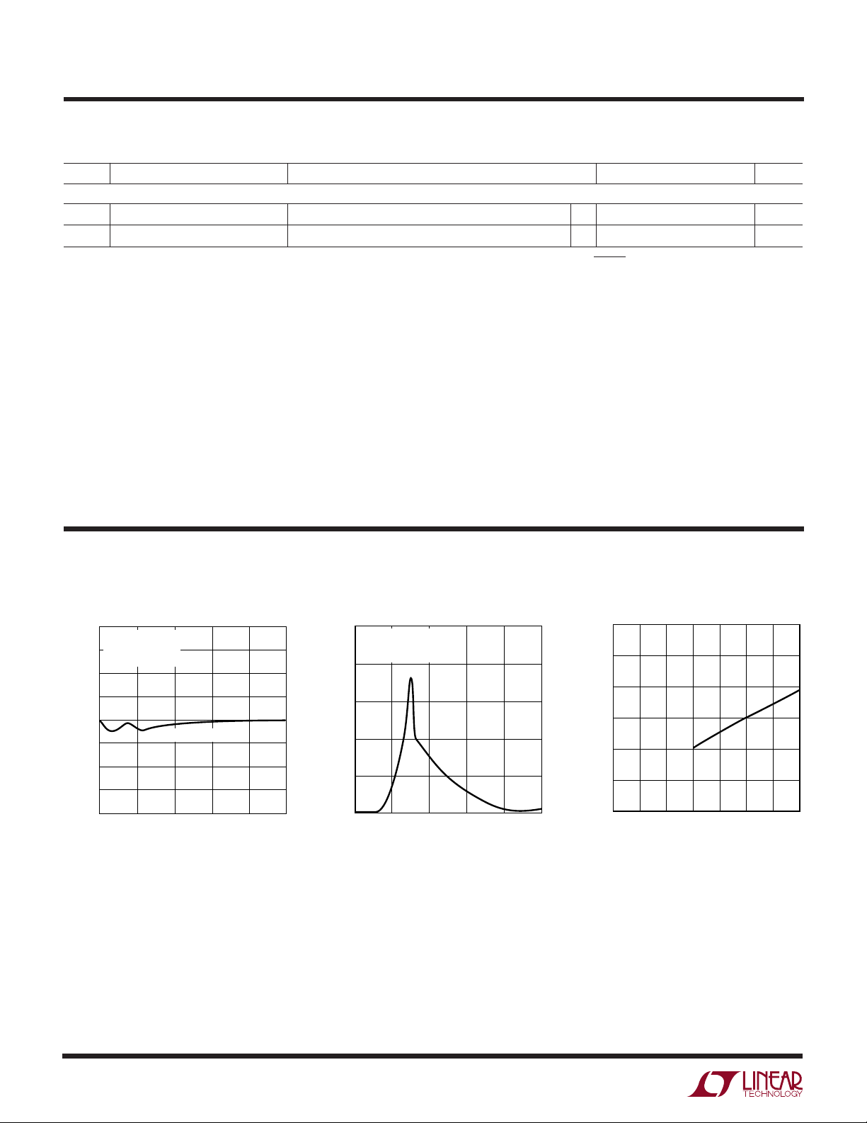
TYPICAL PERFOR A CE CHARACTERISTICS
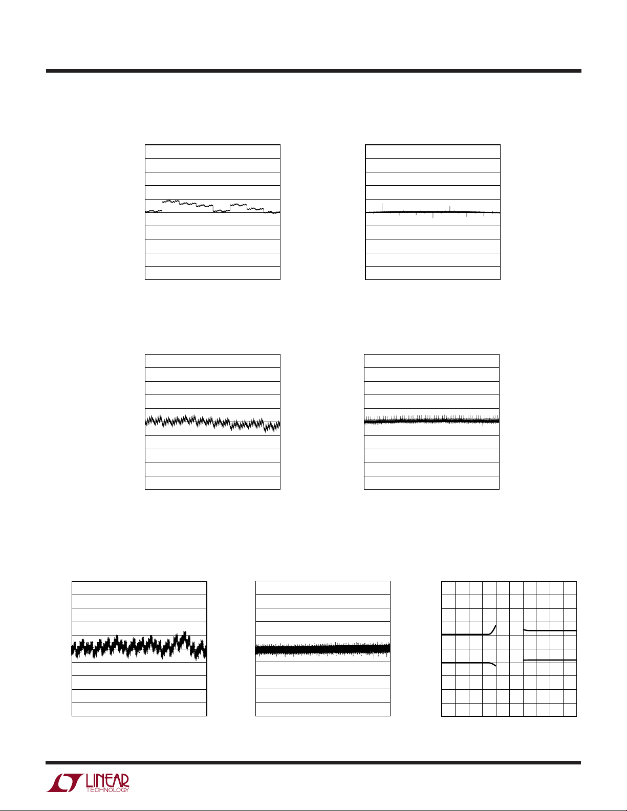
Midscale Glitch Impulse
40
USING AN LT1468
= 30pF
C
FEEDBACK
30
V
= 10V
REF
20
10
0
–10
OUTPUT VOLTAGE (mV)
–20
–30
–40
0
1nV-s TYPICAL
0.2 0.4 0.8
TIME (µs)
0.6
1.0
1588992 G03
Supply Current vs Input Voltage
5
VCC = 5V
ALL DIGITAL INPUTS
TIED TOGETHER
4
3
2
SUPPLY CURRENT (mA)
1
0
1
0
INPUT VOLTAGE (V)
3
2
4
(LTC1588/LTC1589/LTC1592)
Logic Threshold vs Supply Voltage
3.0
2.5
2.0
1.5
1.0
LOGIC THRESHOLD (V)
0.5
0
1588992 G09
5
0
234
1
SUPPLY VOLTAGE (V)
576
1588992 G10
4
1588992fa
LTC1588/LTC1589/LTC1592
UW
TYPICAL PERFOR A CE CHARACTERISTICS
(LTC1588)
Integral Nonlinearity Differential Nonlinearity
(LTC1589)
1.0
0.8
0.6
0.4
0.2
0
–0.2
–0.4
–0.6
INTEGRAL NONLINEARITY (LSB)
–0.8
–1.0
800
0
DIGITAL INPUT CODE
2400 3200 4095
1600
1588992 G11
Integral Nonlinearity Differential Nonlinearity
1.0
0.8
0.6
0.4
0.2
0
–0.2
–0.4
–0.6
INTEGRAL NONLINEARITY (LSB)
–0.8
–1.0
0
4112
8224 12336 16383
DIGITAL INPUT CODE
1588992 G13
1.0
0.8
0.6
0.4
0.2
0
–0.2
–0.4
–0.6
DIFFERENTIAL NONLINEARITY (LSB)
–0.8
–1.0
0
1.0
0.8
0.6
0.4
0.2
0
–0.2
–0.4
–0.6
DIFFERENTIAL NONLINEARITY (LSB)
–0.8
–1.0
0
800
1600
DIGITAL INPUT CODE
4112
8224 12336 16383
DIGITAL INPUT CODE
2400 3200 4095
1588992 G12
1588992 G14
(LTC1592)
Integral Nonlinearity (INL)
1.0
0.8
0.6
0.4
0.2
0
–0.2
–0.4
–0.6
INTEGRAL NONLINEARITY (LSB)
–0.8
–1.0
0
16384
DIGITAL INPUT CODE
32768
49152
1588992 G01
65535
Differential Nonlinearity (DNL)
1.0
0.8
0.6
0.4
0.2
0
–0.2
–0.4
–0.6
DIFFERENTIAL NONLINEARITY (LSB)
–0.8
–1.0
0
16384
32768
DIGITAL INPUT CODE
49152
65535
1588992 G02
Integral Nonlinearity
vs Reference Voltage
in Unipolar Mode
1.0
0.8
0.6
0.4
0.2
0
–0.2
–0.4
–0.6
INTEGRAL NONLINEARITY (LSB)
–0.8
–1.0
–6
–4
–8 8
–10
–2
0
REFERENCE VOLTAGE (V)
2
4
6
10
1588992 G05
1588992fa
5
LTC1588/LTC1589/LTC1592
UW
TYPICAL PERFOR A CE CHARACTERISTICS
(LTC1592)
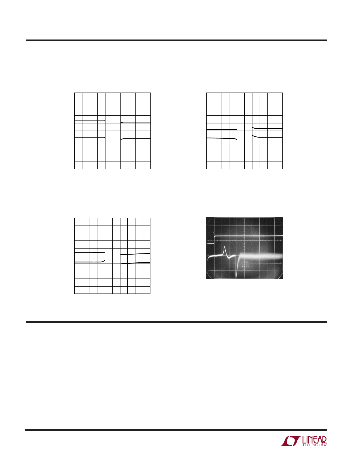
Integral Nonlinearity
vs Reference Voltage
in Bipolar Mode
1.0
0.8
0.6
0.4
0.2
0
–0.2
–0.4
–0.6
INTEGRAL NONLINEARITY (LSB)
–0.8
–1.0
–6
–4
–8 8
–10
–2
0
REFERENCE VOLTAGE (V)
Differential Nonlinearity
vs Reference Voltage
in Bipolar Mode
1.0
0.8
0.6
0.4
0.2
0
–0.2
–0.4
–0.6
DIFFERENTIAL NONLINEARITY (LSB)
–0.8
–1.0
–6
–4
–8 8
–10
–2
0
REFERENCE VOLTAGE (V)
Differential Nonlinearity
vs Reference Voltage
in Unipolar Mode
1.0
0.8
0.6
0.4
0.2
0
–0.2
–0.4
–0.6
DIFFERENTIAL NONLINEARITY (LSB)
–0.8
2
4
6
10
1588992 G06
–1.0
–6
–4
–8 8
–10
–2
REFERENCE VOLTAGE (V)
2
4
6
0
10
1588992 G07
Full-Scale Settling Waveform
LD PULSE
5V/DIV
GATED
SETTLING
WAVEFORM
500µV/DIV
500ns/DIV
USING LT1468 OP AMP
= 20pF
C
2
4
6
10
1588992 G08
FEEDBACK
0V TO 10V STEP
1592 G04
U
UU
PI FU CTIO S
R
(Pin 1): Center Tap Point of the Two Bipolar Resis-
COM
tors R1 and R2. Normally tied to the inverting input of an
external amplifier. When these resistors are not used,
connect this pin to ground. The absolute maximum voltage range on this pin is –0.3V to 12V.
R1 (Pin 2): Bipolar Resistor R1. The main reference input
V
, typically 5V. Accepts up to ±15V. Normally tied to
REF
R
(Pin 3) and the reference input voltage V
OFS
REF
(5V).
When not used connect this pin to ground.
6
R
(Pin 3): Bipolar Offset Network. This pin provides the
OFS
offset of the output voltage range for bipolar modes.
Accepts up to ±15V. Normally tied to R1 and the reference
input voltage V
driven from a different voltage than V
(5V). Alternatively, this pin may be
REF
.
REF
RFB (Pin 4): Feedback Network. Normally tied to the output
of the current to voltage converter op amp. Range limited
to ±15V.
1588992fa
 Loading...