

Linear LTC1474, LTC1475, LTC1474-3.3, LTC1474-5, LTC1475-3.3 Demo Manual
...
DEMO MANUAL DC143
U
DESCRIPTIO
This demonstration circuit is a step-down (buck) regulator
using the LTC®1474/LTC1475. The exclusive use of surface
mount components and the LTC1474/LTC1475 in the tiny
MSOP package results in a highly efficient application in a
small board space. This demo board highlights the
capabilities of the LTC1474/LTC1475, which use a current
mode, constant off-time architecture to switch an internal
P-channel power MOSFET. This results in a power supply
that has low ripple and fast transient response. At low
output currents the LTC1474/LTC1475 automatically
switch to Burst ModeTM operation to maintain high operating
efficiencies and minimize supply current. At no load,only
DEMO MANUAL DC143
NO DESIGN SWITCHER
LTC1474/LTC1475
10µA I
, High Efficiency,
Q
Step-Down DC/DC
Converter
10µA (typical) is required to regulate the output. The parts
can be shut down to further reduce the supply current to
6µA (typical). In dropout, the internal P-channel MOSFET
is turned on continuously (100% duty cycle), providing
low dropout operation with V
battery detector allows the user to monitor the input
supply through an external resistive divider. This board is
intended for applications such as cellular phones, GSM
systems, 4mA to 20mA current-loop pirate supplies or any
portable battery-powered application. Gerber files for this
circuit board are available. Call the LTC factory.
, LTC and LT are registered trademarks of Linear Technology Corporation.
Burst Mode is a trademark of Linear Technology Corporation.
≅ VIN. An onboard low-
OUT
UW
WW
PERFORmANCE SU ARY
SYMBOL PARAMETER CONDITIONS BOARD SUFFIX VALUE
V
V
I
I
IN
OUT
OUT
Q
Input Voltage Range V
Output Voltage LTC1474/LTC1475 A, D 3.3V ± 0.10V
Maximum Output Current R
Typical Supply Current VIN = 10V, I
U
W
= 3.3V A, B, D, E 3.3V to 18V
OUT
= 5V C, F 5V to 18V
V
OUT
LTC1474-3.3/LTC1475-3.3 B, E 3.3V ± 0.10V
LTC1474-5/LTC1475-5 C, F 5V ± 0.15V
= 0Ω ALL 300mA
SENSE
= 0.25Ω ALL 150mA
R
SENSE
= 0 A, B, C 10µA
LOAD
V
IN
= 10V, I
= 0 D, E, F 15µA
LOAD
U
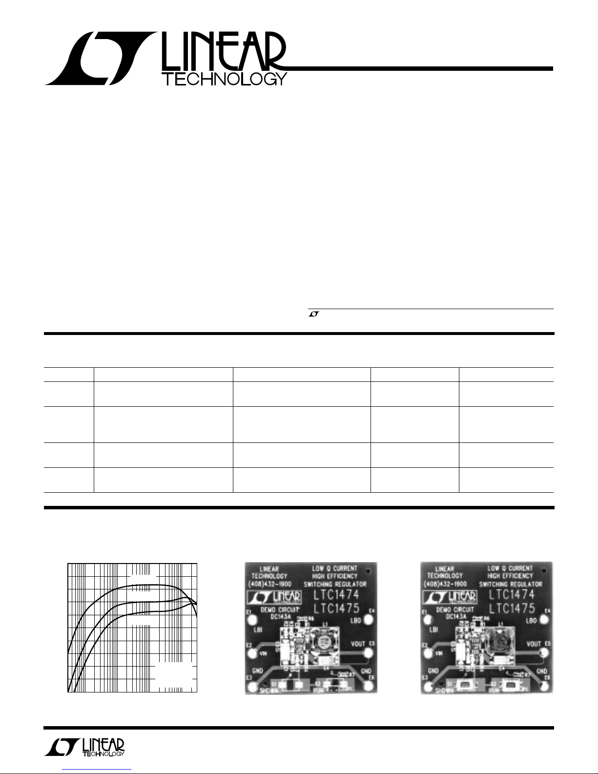
TYPICAL PERFOR A CE CHARACTERISTICS A D BOARD PHOTO
Board A, B, D, E Efficiency Demo Board A
100
VIN = 5V
90
80
VIN = 10V
VIN = 15V
Demo Board D
70
EFFICIENCY (%)
60
50
0.03 3 30 300
0.3
LOAD CURRENT (mA)
L = 100µH
= 3.3V
V
OUT
R
= 0Ω
SENSE
DM143 TPC
DM143 DB A
DM143 DB D
1
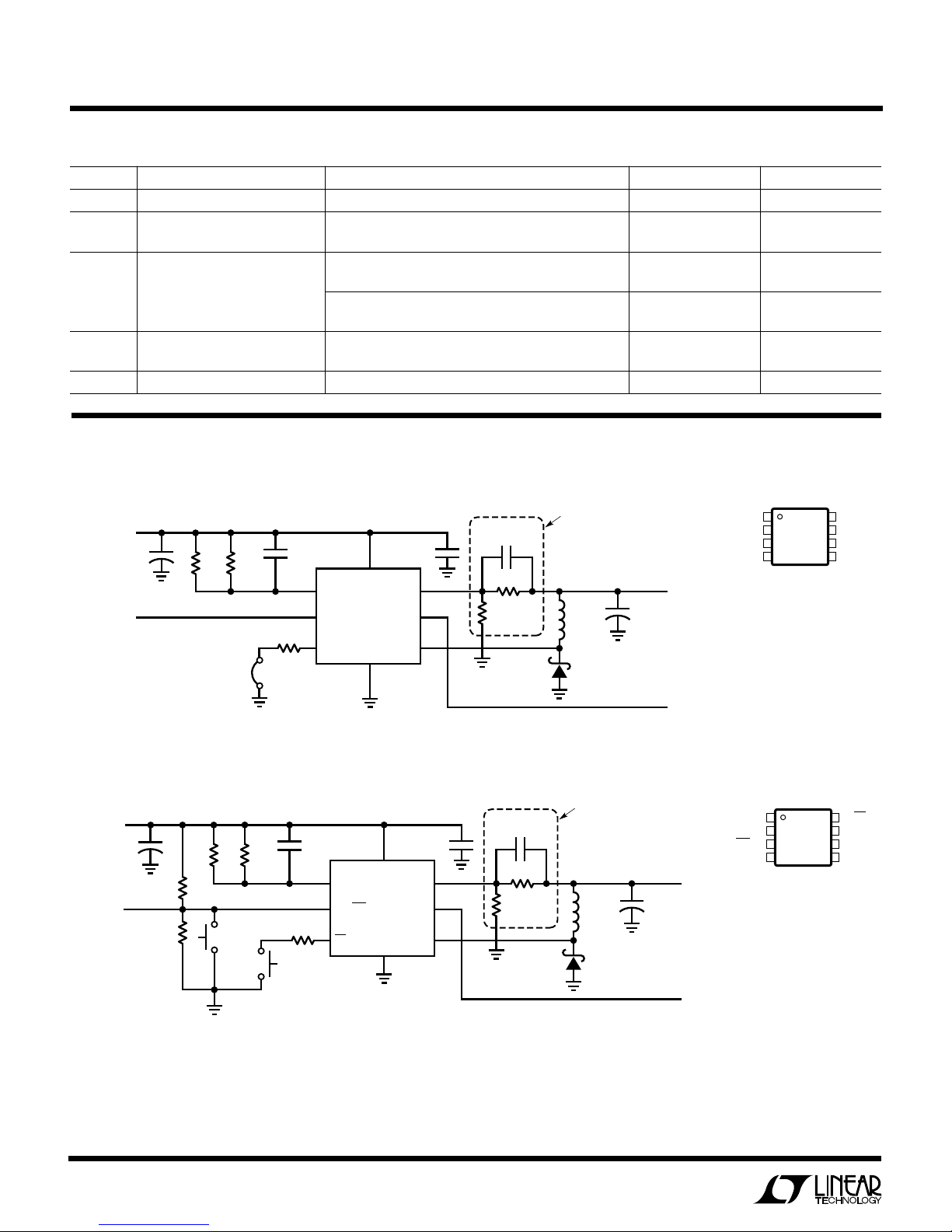
DEMO MANUAL DC143
1
2
3
4
V
OUT
(VFB*)
LBO
LBI
GND
8
7
6
5
RUN
V
IN
SENSE
SW
TOP VIEW
MS8 PACKAGE
8-LEAD PLASTIC MSOP
*ADJUSTABLE OUTPUT VERSION
UW
WW
PERFORmANCE SU ARY
SYMBOL PARAMETER CONDITIONS BOARD SUFFIX VALUE
V
RIPPLE
∆V
V
LBI
OUT
Typical Output Ripple I
Typical Line Regulation 4V < VIN < 18V, R
Typical Load Regulation 0 < I
= 100mA All 50mV
OUT
< 18V, R
4V < V
IN
4V < VIN < 18V, R
4V < VIN < 18V, R
6V < VIN < 18V, R
< 18V, R
6V < V
IN
< 300mA, R
LOAD
0 < I
< 150mA, R
LOAD
SENSE
SENSE
SENSE
SENSE
SENSE
SENSE
= 0Ω, I
= 0.25Ω, I
= 0Ω, I
= 0.25Ω, I
= 0Ω, I
= 0.25Ω, I
SENSE
SENSE
= 100mA A, D 35mV
LOAD
= 100mA 25mV
LOAD
= 100mA B, E 20mV
LOAD
= 100mA 10mV
LOAD
= 100mA C, F 20mV
LOAD
= 100mA 10mV
LOAD
= 0Ω, VIN = 10V All 10mV
= 0.25Ω, VIN = 10V 10mV
Low-Battery Trip Threshold All 1.23V
W UW
PACKAGE A D SCHE ATIC DIAGRA SM
VIN
4V* TO 18V
LBI
*3.3V AT NO LOAD
4.7µF
35V
C3
+
C1
R6
0Ω
JP1
RUN
R1
0.25Ω
R7
100k
C2
1000pF
6
3
8
SENSE
LBI
RUN
7
V
IN
LTC1474
GND
4
V
LBO
SW
0.1µF
FB
C5
1
2
5
10pF
R5
R4
THIS NETWORK
IS PRESENT IN
BOARD A ONLY
+
L1
100µH
D1
MBR0530
C4
100µF
6.3V
V
OUT
3.3V
300mA
LBO
DM143 F01
LTC1474CMS8
LTC1474CMS8-3.3
LTC1474CMS8-5
Figure 1. LTC1474 Demo Board Schematic
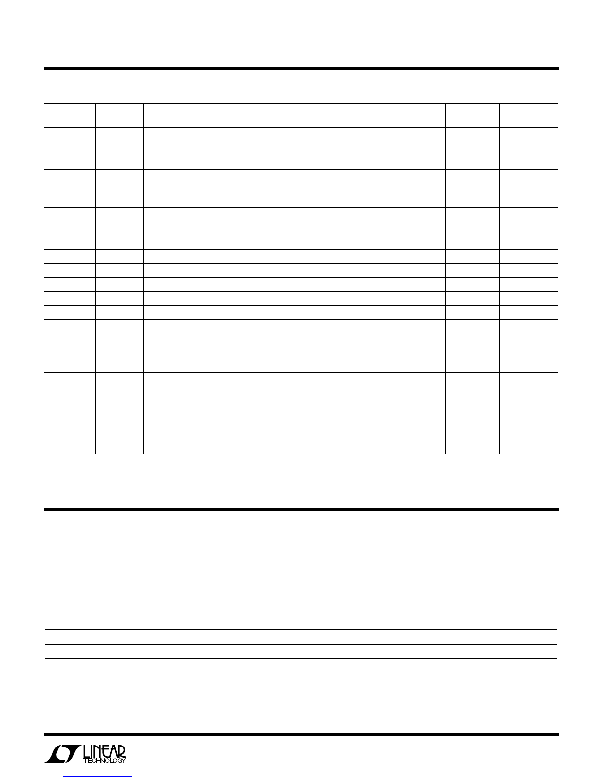
VIN
4V* TO 18V
4.7µF
LBI
*3.3V AT NO LOAD
35V
+
C1
3.01M
1M
R3
R2
R6
0Ω
SHDN
R1
0.25Ω
R7
100kRUN
C2
1000pF
Figure 2. LTC1475 Demo Board Schematic
2
6
3
8
SENSE
LBI/OFF
ON
7
V
IN
LTC1475
GND
4
V
LBO
SW
0.1µF
FB
C3
C5
1
2
5
10pF
R5
R4
THIS NETWORK
IS PRESENT IN
BOARD D ONLY
+
L1
100µH
D1
MBR0530
C4
100µF
6.3V
V
OUT (VFB
LBO
LBI/OFF
GND
V
OUT
3.3V
300mA
*ADJUSTABLE OUTPUT VERSION
TOP VIEW
1
*)
2
3
4
MS8 PACKAGE
8-LEAD PLASTIC MSOP
LTC1475CMS8
LTC1475CMS8-3.3
8
7
6
5
ON
V
IN
SENSE
SW
LTC1475CMS8-5
LBO
DM143 F02
DEMO MANUAL DC143
PARTS LIST
REFERENCE
DESIGNATOR QUANTITY PART NUMBER DESCRIPTION VENDOR TELEPHONE
C1 1 TPSC475M035 4.7µF 35V 20% Tantalum Capacitor AVX (207) 282-5111
C2 1 080553102KAT2A 1000pF 25V 10% X7R Capacitor AVX (803) 946-0362
C3 1 08055310KAT1A 10pF 25V 10% NPO Capacitor (Boards B, C, E, F Only) AVX (803) 946-0362
C4 1 TPSC107M006R0150 100µF 6.3V 20% Tantalum Capacitor (Boards A, B, D, E) AVX (207) 282-5111
TPSC336M010R0375 33µF 6.3V 20% Tantalum Capacitor (Boards C, F)
C5 1 08053E104ZAT1A 0.1µF 25V +80% to –20% Y5V Capacitor AVX (803) 946-0362
D1 1 MBR0530 0.5A 30V Schottky Diode Motorola (602) 244-3576
E1 to E6 6 2501-02 Terminal Turret Mill Max (516) 922-6000
JP1 1 2802S-02-G2 Connector Pin Header (Boards A, B, C) Comm Con (818) 301-4200
L1 1 CDRH73-101 100µH Inductor Sumida (847) 956-0666
R1 1 LR1206 01 R250 F0 0.25Ω 0.25W 1% Resistor IRC (512) 992-7900
R2 1 CR21-105J-T 1M 0.1W 5% Resistor (Boards D, E, F Only) AVX (803) 946-0524
R3 1 CR21-225J-T 2.2M 0.1W 5% Resistor (Boards D, E, F Only) AVX (803) 946-0524
R4 1 WCR0805-1474-F-P-LT 1.47M 0.1W 1% Resistor (Boards B, C, E, F Only) IRC (512) 992-7900
R5 1 CJ21-000J-T 0805 Shunt Resistor (Boards B, C, E, F) AVX (803) 946-0524
WCR0805-2494-F-P-LT 2.49M 0.1W 1% Resistor (Boards A, D) IRC (512) 992-7900
R6 1 CJ21-000J-T 0805 Shunt Resistor AVX (803) 946-0524
R7 1 CR21-104J-T 100k 0.1W 5% Resistor AVX (803) 946-0524
S1, S2 2 EVQ PJS05K Momentary Switch (Boards D, E, F) Panasonic (201) 392-4511
U1 1 LTC1474CMS8 8-Pin MSOP IC, LTC1474 (Board A) LTC (408) 432-1900
LTC1474CMS8-3.3 8-Pin MSOP IC, LTC1474-3.3 (Board B)
LTC1474CMS8-5 8-Pin MSOP IC, LTC1474-5 (Board C)
LTC1475CMS8 8-Pin MSOP IC, LTC1475 (Board D)
LTC1475CMS8-3.3 8-Pin MSOP IC, LTC1475-3.3 (Board E)
LTC1475CMS8-5 8-Pin MSOP IC, LTC1475-5 (Board F)
Table 1. Demo Board Version Cross Reference
BOARD SUFFIX PART NUMBER OUTPUT VOLTAGE ON/OFF CONTROL
A LTC1474 3.3V (Adjustable) Jumper
B LTC1474-3.3 3.3V Jumper
C LTC1474-5 5V Jumper
D LTC1475 3.3V (Adjustable) Pushbutton
E LTC1475-3.3 3.3V Pushbutton
F LTC1475-5 5V Pushbutton
3
 Loading...