

Linear LT6106 Schematic [ru]
LT6106
36V Low Cost High Side
Current Sense in a SOT-23
FEATURES
■
Gain Confi gurable with Two Resistors
■
Low Offset Voltage: 250μV Maximum
■
Output Current: 1mA Maximum
■
Supply Range: 2.7V to 36V, 44V Absolute Maximum
■
Low Input Bias Current: 40nA Maximum
■
PSRR: 106dB Minimum
■
Low Supply Current: 65μA Typical, V+ = 12V
■
Operating Temperature Range: –40°C to 125°C
■
Low Profi le (1mm) ThinSOTTM Package
APPLICATIONS
■
Current Shunt Measurement
■
Battery Monitoring
■
Power Management
■
Motor Control
■
Lamp Monitoring
■
Overcurrent and Fault Detection
DESCRIPTION
The LT®6106 is a versatile high side current sense amplifi er. Design fl exibility is provided by the excellent device
characteristics: 250μV maximum offset and 40nA maximum input bias current. Gain for each device is set by two
resistors and allows for accuracy better than 1%.
The LT6106 monitors current via the voltage across an
external sense resistor (shunt resistor). Internal circuitry
converts input voltage to output current, allowing for a
small sense signal on a high common mode voltage to
be translated into a ground referenced signal. The low DC
offset allows for monitoring very small sense voltages. As
a result, a small valued shunt resistor can be used, which
minimizes the power loss in the shunt.
The wide 2.7V to 44V input voltage range, high accuracy
and wide operating temperature range make the LT6106
ideal for automotive, industrial and power management
applications. The very low power supply current of the
LT6106 also makes it suitable for low power and battery
operated applications.
, LT, LTC and LTM are registered trademarks of Linear Technology Corporation.
ThinSOT is a trademark of Linear Technology Corporation. All other trademarks are the
property of their respective owners.
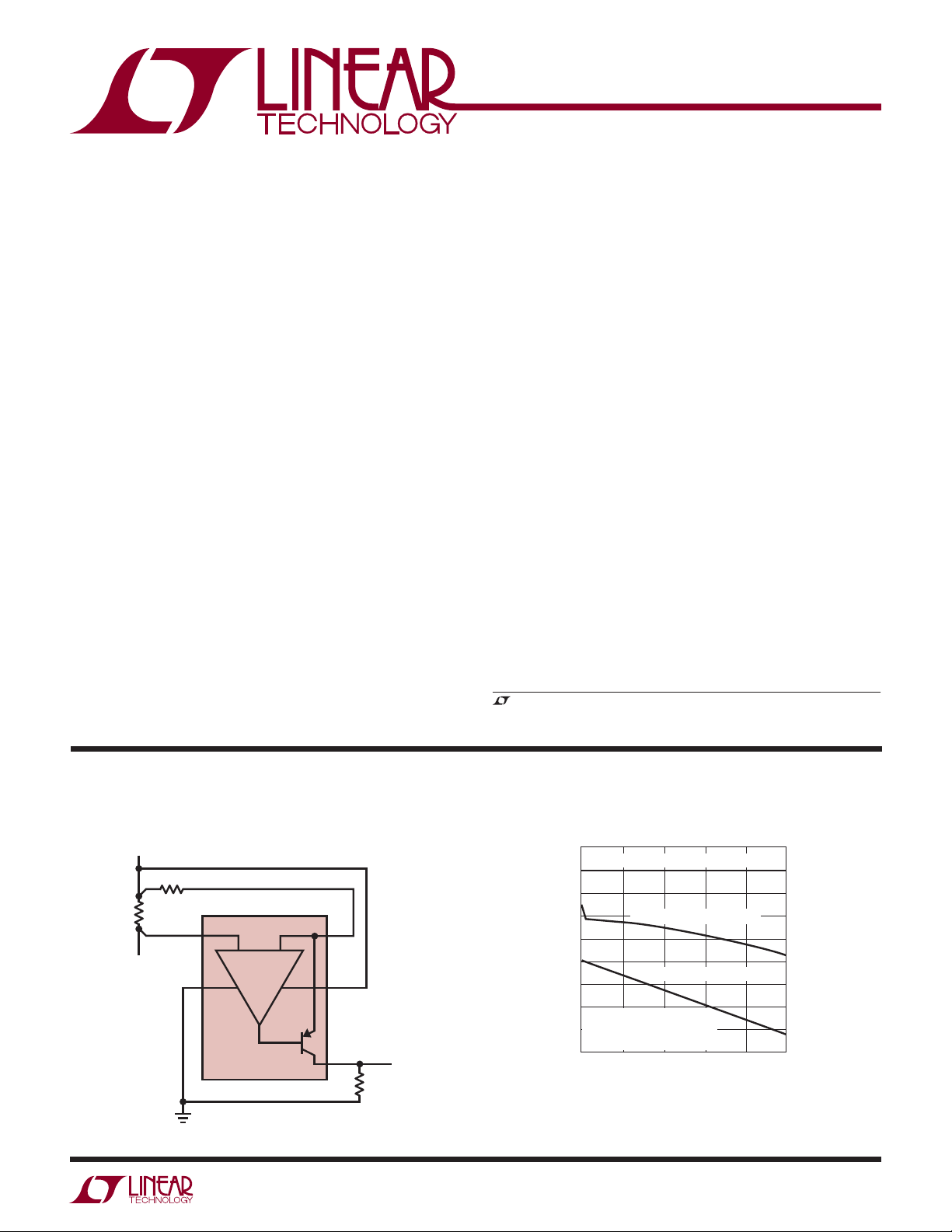
TYPICAL APPLICATION
3V to 36V, 5A Current Sense with AV = 10
3V TO 36V
LOAD
100Ω
–
+
–
V
LT6106
0.02Ω
–IN+IN
+
V
OUT
6106 TA01a
Measurement Accuracy vs Load Current
0.6
0.4
0.2
0
–0.2
–0.4
–0.6
–0.8
ACCURACY (% OF FULL SCALE)
–1.0
V
OUT
200mV/A
1k
–1.2
LIMIT OVER TEMPERATURE
TYPICAL PART AT TA = 25°C
LIMIT OVER TEMPERATURE
5A FULL SCALE
= 0.02Ω
R
SENSE
= 10
A
V
0
RIN = 100Ω
= 1k
R
OUT
+
= 3V
V
13
2
LOAD CURRENT (A)
4
5
6106 TA01b
6106fa
1
LT6106
PIN CONFIGURATIONABSOLUTE MAXIMUM RATINGS
(Note 1)
Supply Voltage (V+ to V–)..........................................44V
–
Input Voltage (+IN to V
) ............................................ V
(–IN to V–) ............................................ V
Input Current ........................................................–10mA
Output Short-Circuit Duration .......................... Indefi nite
Operating Temperature Range (Note 4)
LT6106C ............................................... –40°C to 85°C
+
+
OUT 1
TOP VIEW
–
2
V
–IN 3
S5 PACKAGE
5-LEAD PLASTIC TSOT-23
T
= 150°C, θJA = 250°C/W
JMAX
5 V
4 +IN
+
LT6106H ............................................ –40°C to 125°C
Specifi ed Temperature Range (Note 4)
LT6106C ................................................... 0°C to 70°C
LT6106H ............................................ –40°C to 125°C
Storage Temperature Range ................... –65°C to 150°C
Lead Temperature (Soldering, 10 sec) ..................300°C
ORDER INFORMATION
Lead Free Finish
TAPE AND REEL (MINI) TAPE AND REEL PART MARKING* PACKAGE DESCRIPTION TEMPERATURE RANGE
LT6106CS5#TRMPBF LT6106CS5#TRPBF LTCWK 5-Lead Plastic TSOT-23 0°C to 70°C
LT6106HS5#TRMPBF LT6106HS5#TRPBF LTCWK 5-Lead Plastic TSOT-23 –40°C to 125°C
TRM = 500 pieces. *Temperature grades are identifi ed by a label on the shipping container.
Consult LTC Marketing for parts specifi ed with wider operating temperature ranges.
Consult LTC Marketing for information on lead based fi nish parts.
For more information on lead free part marking, go to: http://www.linear.com/leadfree/
For more information on tape and reel specifi cations, go to: http://www.linear.com/tapeandreel/
ELECTRICAL CHARACTERISTICS
The ● denotes the specifi cations which apply over the full specifi ed
operating temperature range, otherwise specifi cations are at TA = 25°C. V+ = 12V, V+ = V
SENSE
+, R
= 100Ω, R
IN
= 10k, Gain = 100
OUT
unless otherwise noted. (Note 6)
SYMBOL PARAMETER CONDITIONS MIN TYP MAX UNITS
+
V
V
OS
/ΔT Input Offset Voltage Drift V
ΔV
OS
I
B
I
OS
I
OUT
PSRR Power Supply Rejection Ratio V
V
SENSE(MAX)
Error Gain Error (Note 3) V
A
V
V
OUT(HIGH)
Supply Voltage Range
Input Offset Voltage V
Input Bias Current (+IN) V+ = 12V, 36V
Input Offset Current V+ = 12V, 36V 1 nA
Maximum Output Current (Note 2)
Input Sense Voltage Full Scale RIN = 500Ω (Notes 2, 7)
Output Swing High
(Referred to V
+
)
= 5mV
SENSE
= 5mV
SENSE
+
= 2.7V to 36V, V
= 500mV, RIN = 500Ω, R
SENSE
= 500mV, RIN = 500Ω, R
V
SENSE
= 120mV
V
SENSE
SENSE
= 5mV
= 10k, V+ = 12.5V
OUT
= 10k, V+ = 36V
OUT
●
2.7 36 V
●
●
●
●
1mA
●
106 dB
●
0.5 V
●
–0.65 –0.25 0 %
●
–0.45 –0.14 0.1 %
●
150 250
350
1μV/°C
40
65
1.2
1.4
μV
μV
nA
nA
6106fa
2
V
V
LT6106
ELECTRICAL CHARACTERISTICS
The ● denotes the specifi cations which apply over the full specifi ed
operating temperature range, otherwise specifi cations are at TA = 25°C. V+ = 12V, V+ = V
unless otherwise noted.
SYMBOL PARAMETER CONDITIONS MIN TYP MAX UNITS
Minimum Output Voltage
(Note 5)
BW Signal Bandwidth (–3dB) I
t
r
Input Step Response (to 50% of
Output Step)
I
S
Supply Current V+ = 2.7V, I
= 0mV, RIN = 100Ω, R
V
SENSE
V
= 0mV, RIN = 500Ω, R
SENSE
= 1mA, RIN = 100Ω, R
OUT
ΔV
= 100mV Step, RIN = 100Ω, R
SENSE
Rising Edge
= 0μA, (V
OUT
+
= 12V, I
V
V+ = 36V, I
= 0μA, (V
OUT
= 0μA, (V
OUT
SENSE
SENSE
= 10k
OUT
= 10k, V+ = 12V, 36V
OUT
= 5k 200 kHz
OUT
= 5k,
OUT
= –5mV)
SENSE
= –5mV)
= –5mV)
SENSE
+, R
●
●
●
●
●
= 100Ω, R
IN
= 10k, Gain = 100
OUT
12 45
65
71622mV
3.5 μs
60 85
115
65 95
120
70 100
130
mV
mV
mV
μA
μA
μA
Note 1: Stresses beyond those listed under Absolute Maximum Ratings
may cause permanent damage to the device. Exposure to any Absolute
Maximum Rating condition for extended periods may affect device
reliability and lifetime. In addition to the Absolute Maximum Ratings, the
output current of the LT6106 must be limited to insure that the power
dissipation in the LT6106 does not allow the die temperature to exceed
150°C. See the applications information section “Power Dissipation
Considerations” for further information.
Note 2: Guaranteed by the gain error test.
Note 3: Gain error refers to the contribution of the LT6106 internal circuitry
and does not include errors in the external gain setting resistors.
characterized and expected to meet specifi ed performance from –40°C to
85°C but is not tested or QA sampled at these temperatures. The LT6106H
is guaranteed to meet specifi ed performance from –40°C to 125°C.
Note 5: The LT6106 output is an open collector current source. The
minimum output voltage scales directly with the ratio R
Note 6: V
R
Note 7: V
. See Figure 1.
SENSE
SENSE
SENSE (MAX)
Characteristics will apply. Higher voltages can affect performance but will
not damage the part provided that the output current of the LT6106 does
not exceed the allowable power dissipation as described in Note 1.
Note 4: The LT6106C is guaranteed functional over the operating
temperature range of –40°C to 85°C. The LT6106C is designed,
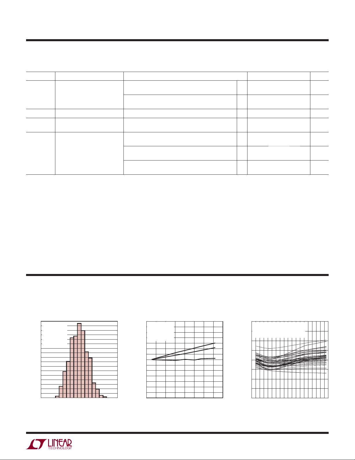
TYPICAL PERFORMANCE CHARACTERISTICS
Input Offset Voltage vs
VOS Distribution
V+ = 12V
16
14
12
10
8
6
PERCENT OF UNITS (%)
4
2
0
= 5mV
V
SENSE
= 100Ω
R
IN
= 10k
R
OUT
1068 UNITS
–120
–200
INPUT OFFSET VOLTAGE (μV)
–40 0
40
120
200
6106 G23
Supply Voltage
70
V
SENSE
60
= 100Ω
R
IN
50
R
OUT
40
TYPICAL UNITS
30
20
10
0
–10
–20
–30
–40
–50
CHANGE IN INPUT OFFSET VOLTAGE (μV)
–60
–70
0
= 5mV
= 10k
5
10
SUPPLY VOLTAGE (V)
20
25
15
30
/10k.
OUT
+
is the voltage at the high side of the sense resistor,
is the maximum sense voltage for which the Electrical
Input Offset Voltage vs
Temperature
35
6106 G02
400
V
SENSE
+
= 12V
V
300
= 100Ω
R
IN
200
100
0
–100
–200
INPUT OFFSET VOLTAGE (μV)
–300
40
–400
–55
–25 5
R
= 5mV
OUT
= 100
A
V
TYPICAL UNITS
TEMPERATURE (°C)
= 10k
35 65
125
95
6106 G03
6106fa
3
LT6106
0
TYPICAL PERFORMANCE CHARACTERISTICS
Gain Error vs Temperature
0
–0.05
–0.10
–0.15
–0.20
–0.25
–0.30
–0.35
GAIN ERROR (%)
–0.40
–0.45
V
= 1V
OUT
= 1mA
I
–0.50
OUT
= 1k
R
OUT
–0.55
TYPICAL UNIT
–0.60
–45
–25
15
–5
TEMPERATURE (°C)
Gain Error Distribution
24
V+ = 12.5V
22
20
18
16
14
12
10
8
PERCENT OF UNITS (%)
6
4
2
0
–0.60
= 500mV
V
SENSE
= 500Ω
R
IN
= 10k
R
OUT
11,072 UNITS
= 25°C
T
A
–0.48
–0.36
GAIN ERROR (%)
V+ = 36V
V+ = 12V
V+ = 5V
V+ = 2.7V
35
55 75 95 115 130
–0.24
–0.12
6106 G04
6106 G24
Power Supply Rejection Ratio
vs Frequency
120
110
100
90
80
70
60
50
40
30
V
20
POWER SUPPLY REJECTION RATIO (dB)
10
0
100 10k 100k 1M
= 0.5V
OUT
V
= 1V
OUT
= 2V
V
OUT
1k
FREQUENCY (Hz)
V+ = 12.5V
A
R
R
Gain vs Frequency
45
40
35
30
25
20
15
10
5
GAIN (dB)
0
–5
–10
–15
–20
–25
–30
V
= 10V
OUT
V
= 2.5V
OUT
1k 100k 1M 10M
10k
FREQUENCY (Hz)
V+ = 12.5V
A
V
R
IN
R
OUT
= 20
V
= 100Ω
IN
OUT
= 100
= 100Ω
= 10k
= 2k
6106 G08
6106 G09
Power Supply Rejection Ratio
vs Frequency
120
110
100
90
80
70
60
50
40
30
V
20
POWER SUPPLY REJECTION RATIO (dB)
10
0
100 10k 100k 1M
= 2.5V
OUT
= 5V
V
OUT
= 10V
V
OUT
1k
FREQUENCY (Hz)
V+ = 12.5V
A
R
R
Gain vs Frequency
45
40
35
30
25
20
15
10
5
GAIN (dB)
0
–5
–10
–15
–20
–25
–30
1k 100k 1M 10M
V
OUT
V
= 2.5V
OUT
10k
FREQUENCY (Hz)
= 10V
V+ = 12.5V
A
V
R
IN
R
OUT
= 20
V
= 500Ω
IN
OUT
= 20
= 500Ω
= 10k
= 10k
6106 G06
6106 G14
Input Bias Current vs Supply
Voltage
20
V
= 5mV
SENSE
19
= 100Ω
R
IN
18
17
16
15
14
13
INPUT BIAS CURRENT (nA)
12
11
10
105
0
2015
SUPPLY VOLTAGE (V)
4
30 35 45
25
TA = –40°C
= 25°C
T
A
= 70°C
T
A
= 125°C
T
A
40
6106 G05
50
V
SENSE
20mV/DIV
V
OUT
500mV/DIV
Step Response 0mV to 10mV
(RIN = 100Ω)
0V
V
R
V
OUT
OUT
+
= 12V
= 0V TO 1V
= 10k
5μs/DIVAV = 100
6106 G1
V
SENSE
20mV/DIV
V
OUT
500mV/DIV
Step Response 10mV to 20mV
(RIN = 100Ω)
0V
V
R
V
= 100
V
OUT
OUT
+
= 12V
= 1V TO 2V
= 10k
5μs/DIVA
6106 G1
6106fa
 Loading...