

FEATURES
LT3465/LT3465A
1.2MHz/2.4MHz White
LED Drivers with Built-in
Schottky in ThinSOT
U
DESCRIPTIO
■
Inherently Matched LED Current
■
Drives Up to Six LEDs from a 3.6V Supply
■
No External Schottky Diode Required
■
1.2MHz Switching Frequency (LT3465)
■
2.4MHz Switching Frequency Above AM Broadcast
Band (LT3465A)
■
VIN Range: 2.7V to 16V
■
V
OUT(MAX)
■
Automatic Soft-Start (LT3465)
■
Open LED Protection
■
High Efficiency: 81% (LT3465) 79% (LT3465A)
= 30V
Typical
■
Requires Only 0.22µF Output Capacitor
■
Low Profile (1mm) SOT-23
U
APPLICATIO S
■
Cellular Phones
■
PDAs, Handheld Computers
■
Digital Cameras
■
MP3 Players
■
GPS Receivers
®
The LT
3465/LT3465A are step-up DC/DC converters
designed to drive up to six LEDs in series from a Li-Ion cell.
Series connection of the LEDs provides identical LED
currents and eliminates the need for ballast resistors.
These devices integrate the Schottky diode required externally on competing devices. Additional features include
output voltage limiting when LEDs are disconnected, onepin shutdown and dimming control. The LT3465 has
internal soft-start.
The LT3465 switches at 1.2MHz, allowing the use of tiny
external components. The faster LT3465A switches at
2.4MHz. Constant frequency switching results in low input
noise and a small output capacitor. Just 0.22µF is required
for 3-, 4- or 5-LED applications.
The LT3465 and LT3465A are available in the low profile
(1mm) 6-lead SOT-23 (ThinSOT
, LTC and LT are registered trademarks of Linear Technology Corporation. ThinSOT is a
trademark of Linear Technology Corporation. All other trademarks are the property of their
respective owners.
TM
) package.
U
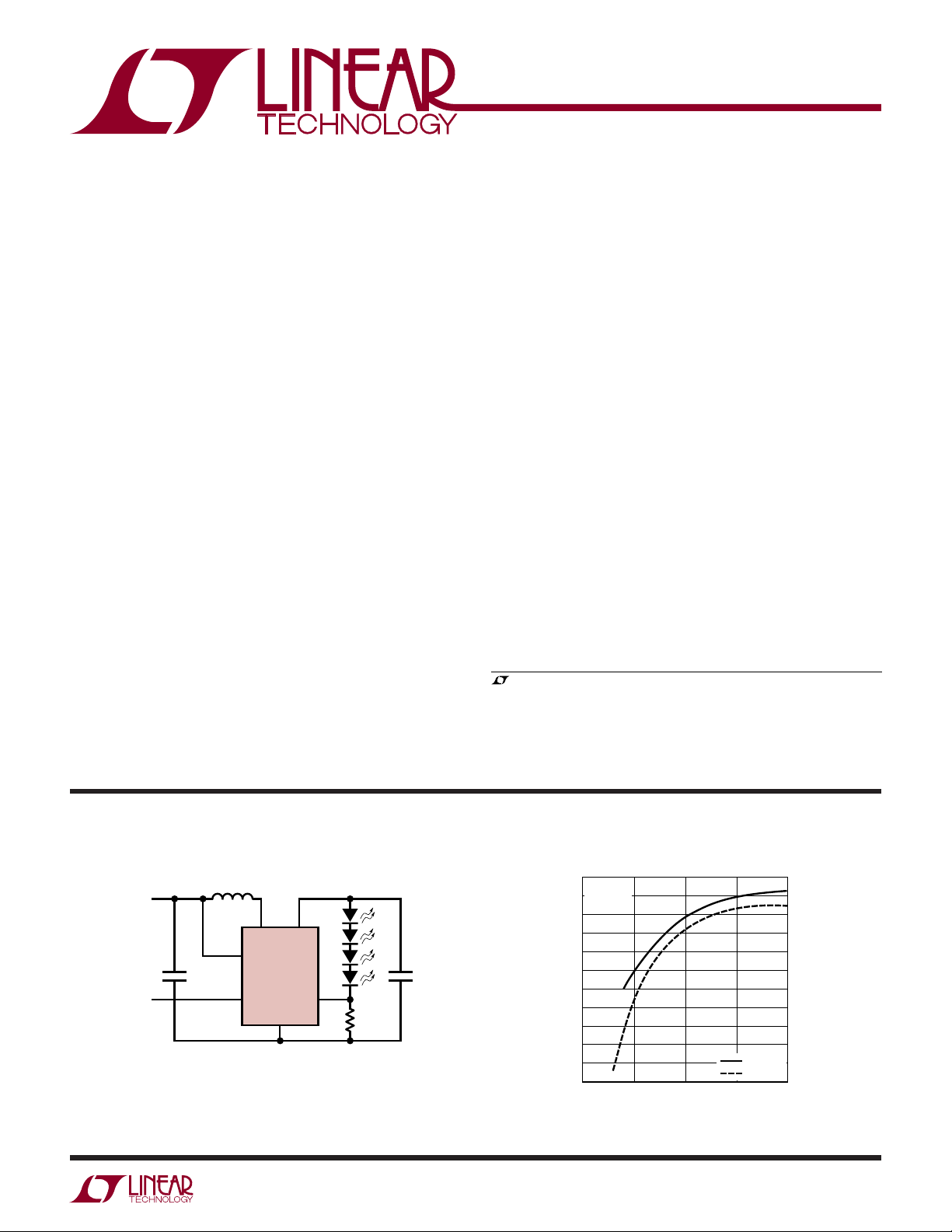
TYPICAL APPLICATIO
L1
22µH
3V TO 5V
SW V
IN
LT3465/
LT3465A
GND
OUT
FB
V
CTRL
SHUTDOWN
AND DIMMING
CONTROL
C1
1µF
C1, C2: X5R OR X7R DIELECTRIC
L1: MURATA LQH32CN220
Figure 1. Li-Ion Powered Driver for Four White LEDs
10Ω
3465A F01a
C2
0.22µF
82
VIN = 3.6V
80
4 LEDs
78
76
74
72
70
68
EFFICIENCY (%)
66
64
62
60
0
Conversion Efficiency
5
10
LED CURRENT (mA)
15
LT3465
LT3465A
20
3465A F01b
3465afa
1
LT3465/LT3465A
WWWU
ABSOLUTE AXI U RATI GS
(Note 1)
Input Voltage (VIN) ................................................. 16V
SW Voltage ............................................................. 36V
FB Voltage ................................................................ 2V
CTRL Voltage .......................................................... 10V
Operating Temperature Range (Note 2) .. – 40°C to 85°C
Maximum Junction Temperature ......................... 125°C
Storage Temperature Range ................ –65°C to 150°C
PACKAGE/ORDER I FOR ATIO
V
1
OUT
GND 2
FB 3
S6 PACKAGE
6-LEAD PLASTIC TSOT-23
T
= 125°C, θJA = 256°C/W IN FREE AIR
JMAX
θ
= 120°C ON BOARD OVER GROUND PLANE
JA
UU
TOP VIEW
6 SW
5 V
IN
4 CTRL
W
Lead Temperature (Soldering, 10 sec)................. 300°C
ORDER PART NUMBER
LT3465ES6
LT3465AES6
Order Options Tape and Reel: Add #TR
Lead Free: Add #PBF Lead Free Tape and Reel: Add #TRPBF
Lead Free Part Marking: http://www.linear.com/leadfree/
Consult LTC Marketing for parts specified with wider operating temperature ranges.
ELECTRICAL CHARACTERISTICS
temperature range, otherwise specifications are at T
PARAMETER CONDITIONS MIN TYP MAX MIN TYP MAX UNITS
Minimum Operating Voltage 2.7 2.7 V
Maximum Operating Voltage 16 16 V
Feedback Voltage 0°C ≤ TA ≤ 85°C 188 200 212 188 200 212 mV
FB Pin Bias Current 10 35 100 10 35 100 nA
Supply Current Not Switching 1.9 2.6 3.3 1.9 2.6 3.3 mA
CTRL = 0V 2.0 3.2 5.0 2.0 3.2 5.0 µA
Switching Frequency 0.8 1.2 1.6 1.8 2.4 2.8 MHz
Maximum Duty Cycle
Switch Current Limit
Switch V
CESAT
Switch Leakage Current VSW = 5V 0.01 5 0.01 5 µA
V
for Full LED Current 1.8 1.8 V
CTRL
V
to Enable Chip
CTRL
V
to Shut Down Chip
CTRL
CTRL Pin Bias Current 48 60 72 48 60 72 µA
Soft-Start Time 600 µs
Schottky Forward Drop ID = 150mA 0.7 0.7 V
Schottky Leakage Current VR = 30V 4 4 µA
ISW = 250mA 300 300 mV
= 85°C 405060405060 µA
T
A
= –40°C 607590607590 µA
T
A
The ● denotes the specifications which apply over the full operating
= 25°C. VIN = 3V, V
A
●
●
●
●
= 3V, unless otherwise noted.
CTRL
LT3465 LT3465A
90 93 90 93 %
225 340 225 340 mA
150 150 mV
50 50 mV
S6 PART MARKING
LTH2
LTAFT
Note 1: Absolute Maximum Ratings are those values beyond which the life
of a device may be impaired.
Note 2: The LT3465E/LT3465AE are guaranteed to meet performance
2
specifications from 0°C to 70°C. Specifications over the –40°C to 85°C
operating temperature range are assured by design, characterization and
correlation with statistical process controls.
3465afa
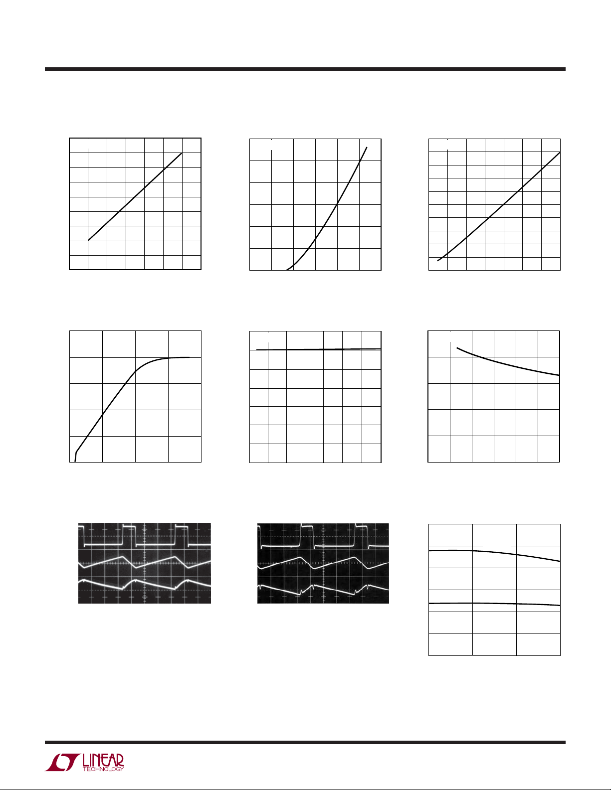
UW
INPUT VOLTAGE (V)
2 2.5
0
INPUT CURRENT (mA)
2
5
3
4
4.5
3465A G06
1
4
3
3.5
5
T
A
= 25°C
TEMPERATURE (°C)
–50
4365A G08
0
50 100
SWITCHING FREQUENCY (MHz)
3.0
2.5
2.0
1.5
1.0
0.5
0
LT3465
LT3465A
TYPICAL PERFOR A CE CHARACTERISTICS
Switch Saturation Voltage (V
450
T
= 25°C
A
400
350
300
250
200
150
100
50
SWITCH SATURATION VOLTAGE (mV)
0
0
100
50
150 350
SWITCH CURRENT (mA)
200
250 300
) Schottky Forward Voltage Drop
CESAT
300
T
= 25°C
A
250
200
150
100
50
SCHOTTKY FORWARD CURRENT (mA)
0
0
3465A G01
400 600 800
200
SCHOTTKY FORWARD DROP (mV)
1000 1200
3465A G02
LT3465/LT3465A
Shutdown Quiescent Current
(CTRL = 0V)
30
T
= 25°C
A
27
24
21
18
15
(µA)
Q
I
12
9
6
3
0
4 6 10 12
2
8
VIN (V)
14
3465A G03
16
VFB vs V
250
200
150
100
FEEDBACK VOLTAGE (mV)
50
0
0
T
CTRL
= 25°C
A
0.5
CONTROL VOLTAGE (V)
Switching Waveforms (LT3465)
V
SW
10V/DIV
I
L
100mA/DIV
V
OUT
100mV/DIV
Open-Circuit Output Clamp Voltage
35
= 25°C
T
A
30
25
20
15
10
OUTPUT CLAMP VOLTAGE (V)
5
1
1.5
2
3465A G04
0
2
46
INPUT VOLTAGE (V)
10 14 16
812
3465A G05
Switching Waveforms (LT3465A)
V
SW
10V/DIV
I
L
50mA/DIV
V
OUT
50mV/DIV
Input Current in Output Open Circuit
Switching Frequency
V
IN
4 LEDs
20mA, 22µH
= 3.6V 200ns/DIV
3465A G07a
V
= 3.6V 100ns/DIV
IN
4 LEDs
20mA, 22µH
3465A G07b
3465afa
3
LT3465/LT3465A
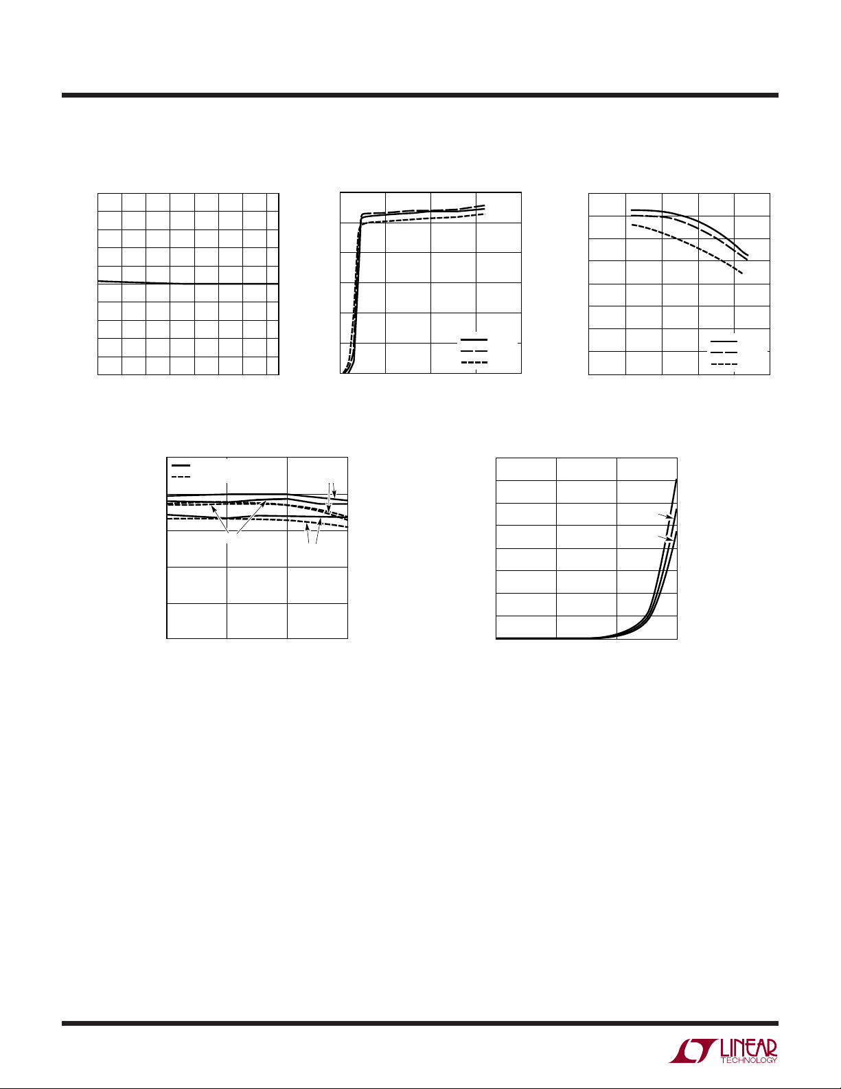
UW
TYPICAL PERFOR A CE CHARACTERISTICS
Feedback Voltage
210
208
206
204
202
200
198
196
FEEDBACK VOLTAGE (mV)
194
192
190
–50
–30 10
–10
TEMPERATURE (°C)
85
80
75
70
EFFICIENCY (%)
65
60
–50
30
50
V
= 3.6V, 4 LEDs
IN
LT3465
LT3465A
15mA
0
TEMPERATURE (°C)
Quiescent Current (CTRL = 3V)
3.0
2.5
2.0
1.5
(mA)
Q
I
1.0
0.5
0
90
70
3465A G09
0
5101520
VIN (V)
–50°C
25°C
100°C
3465A G10
Switching Current Limit
400
350
300
250
200
150
CURRENT LIMIT (mA)
100
50
0
20 40 80
0
DUTY CYCLE (%)
–50°C
25°C
100°C
60
100
3465A G11
Schottky Leakage Current
8
20mA
10mA
50
100
3465A G12
7
6
5
4
3
2
SCHOTTKY LEAKAGE CURRENT (µA)
1
0
–50
050
TEMPERATURE (°C)
V
= 25
R
V
= 16
R
= 10
V
R
100
3465A G13
4
3465afa

LT3465/LT3465A
U
UU
PI FU CTIO S
V
(Pin 1): Output Pin. Connect to output capacitor and
OUT
LEDs. Minimize trace between this pin and output capacitor to reduce EMI.
GND (Pin 2): Ground Pin. Connect directly to local ground
plane.
FB (Pin 3): Feedback Pin. Reference voltage is 200mV.
Connect LEDs and a resistor at this pin. LED current is
determined by the resistance and CTRL pin voltage:
I
LED
⎛
⎜
1
⎜
•–•
200 26 1
=
R
FB
mV mV n
⎜⎜
⎜
⎝
⎛
exp
⎜
⎜
⎜
⎛
ex
pp
⎜
⎜
⎝
⎝
CTRL (Pin 4): Dimming Control and Shutdown Pin. Ground
this pin to shut down the device. When V
than about 1.8V, full-scale LED current is generated.
When V
Floating this pin places the device in shutdown mode.
V
(Pin 5): Input Supply Pin. Must be locally bypassed
IN
with a 1µF X5R or X7R type ceramic capacitor.
SW (Pin 6): Switch Pin. Connect inductor here.
200
mV
⎛
⎜
⎝
26
mV
VmV
()
CTRL
526
•
mV mV
is less than 1V, LED current is reduced.
CTRL
⎞
⎞
⎟
⎠
⎞
⎟
⎟
⎟
⎟
1
+
⎟
⎟
⎞
⎟
⎟
⎟
⎠
⎠
⎠
CTRL
>for V mV
150
is greater
CTRL
3465afa
5
LT3465/LT3465A
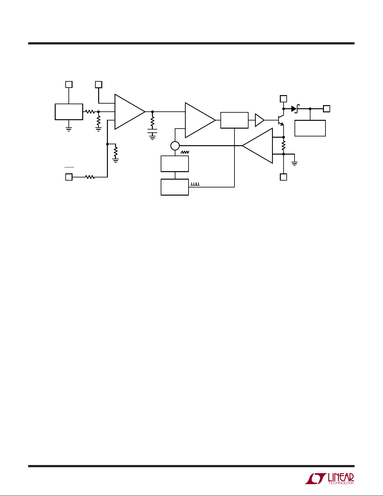
BLOCK DIAGRA
W
V
IN
5
V
REF
1.25V
CTRL
4
40k
FB
3
200mV
SW
–
A1
+
+
R
C
C
C
COMPARATOR
–
A2
+
RQ
S
DRIVER
6
Q1
OVERVOLTAGE
PROTECT
V
OUT
1
+
0.2Ω
–
2
GND
3465A F02
10k
Σ
RAMP
GENERATOR
1.2MHz*
OSCILLATOR
*2.4MHz FOR LT3465A
Figure 2. LT3465 Block Diagram
6
3465afa
 Loading...