

Linear LT2940 Quick Start Manual
DC
-
1495A
1
V
V
A
DEMO
CIRCUIT
1495A
QUICK START GUIDE
0
Power Monitor
DESCRIPTION
LT294
Demonstration circuit 1495A showcases the
LT2940 Power Monitor, configured to measure up
to 30W over a range of 8V to 40V and 0A to 3A.
LEDs indicate when the load power exceeds
12.5W. Power is indicated at PMON with a scaling
factor of 10W/V; IMON indicates current at 1A/V.
All scaling factors and the voltage and current
measurement ranges may be reconfigured by
changing a few resistors. The LT2940’s compara-
tor can monitor either the power output, PMON, or
the current output, IMON.
Design files for this circuit board are available.
Call the LTC factory.
L
, LTC, LTM, LT, Burst Mode, OPTI-LOOP, Over-The-Top and PolyPhase are
registered trademarks of Linear Technology Corporation. Adaptive Power, C-Load,
DirectSense, Easy Drive, FilterCAD, Hot Swap, LinearView, µModule, Micropower
SwitcherCAD, Multimode Dimming, No Latency ∆Σ, No Latency Delta-Sigma, No
R
, Operational Filter, PanelProtect, PowerPath, PowerSOT, SmartStart,
SENSE
SoftSpan, Stage Shedding, SwitcherCAD, ThinSOT, UltraFast and VLDO are trademarks of Linear Technology Corporation. Other product names may be trademarks
of the companies that manufacture the products.
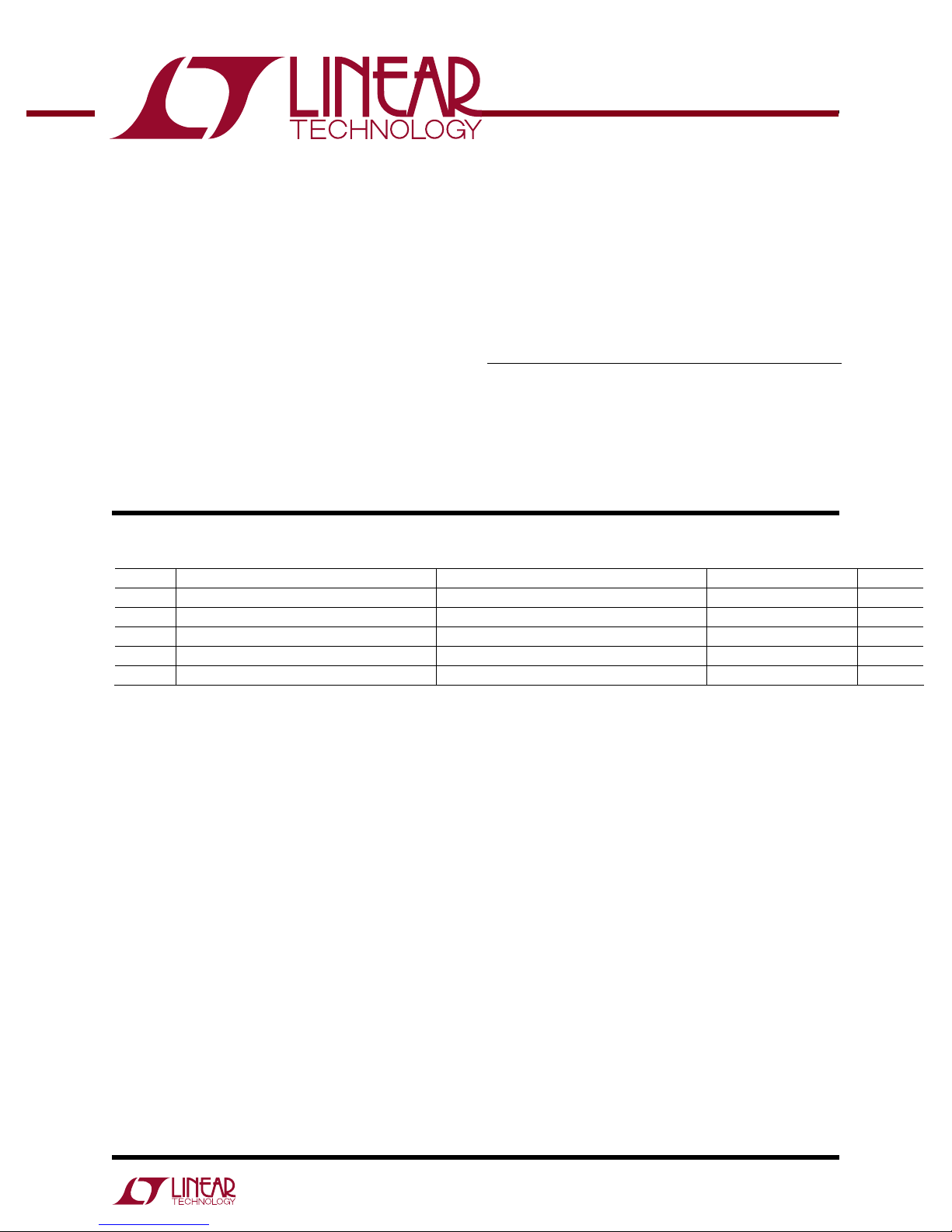
PERFORMANCE SUMMARY
SYMBOL PARAMETER CONDITIONS MIN TYP MAX UNITS
V
IN
V
CC
PMON
IMON
P
TRIP
Input Supply Range
VCC Supply Range (When Separately Powered) 12 80
Load Power for Full Scale Output PMON = 3V
Load Current for Full Scale Output IMON = 3V
Overpower Threshold Red LED Turns On 11 12.5 14 W
Specifications are at TA = 25°C
8 40
27 30 33 W
2.85 3 3.15
OVERVIEW
The LT2940 is a four-quadrant multiplier designed
to measure current and voltage, multiply them, and
produce an output proportional to power. A second output is proportional to the measured current. All inputs and outputs are bipolar; the LT2940
measures positive or negative power, voltage and
current. The power and current outputs operate in
current mode, with a full scale of ±200µA. To facilitate use in a practical application, the current
sense pins (I+ and I–) are designed to operate over
a 4V to 80V common mode range, independent of
the supply pin, VCC. This permits the LT2940 to
measure, for example, a 48V supply while operating on a 12V supply. The LT2940 includes an auxiliary comparator with a fixed 1.25V reference and
complementary outputs.
A distinction must be drawn between the features
and performance of the LT2940, and the features
and performance of DC-1495A. The LT2940 has
the following important features:
●
Four quadrant power measurement with bidirectional power and current outputs
●
VCC-independent, high-side current sense input
●
4V to 80V current sense input operating
range
●
6V to 80V VCC operating range
●
100V absolute maximum rating

DC
-
1495A
2
●
Auxiliary comparator with complementary
outputs
As configured, DC-1495A features:
●
Single quadrant power and current measurement with unidirectional outputs
●
8V to 40V, 0A to 3A measurement range
●
30W full scale power monitor output, 10W/V
●
3A full scale current monitor output, 1A/V
●
75V maximum input, limited by clamp
●
VCC connected to INPUT turret
●
LEDs indicate load power above (red) or below (green) 12.5W
DC-1495A includes provision for optional components, allowing the board to be reconfigured for
different scaling and a variety of applications.
Components
Components are divided into four basic groups:
R12A, R12B, R12C, C1, D1, D2: these components are associated with VCC (D1 supplies constant current to the LEDs). A zero ohm jumper
installed in any one of the R12 positions selects
the source of power for VCC: input, output, or external supply connected to the VCC turret. Use a
resistor if filtering is desired. As built R12B is
stuffed with 10Ω and VCC is bypassed with 100nF,
serving both as a VCC filter and also as a snubber
for the input.
An SMAT70A clamp diode, D2, is connected directly across the input to ground. It has a maximum dc standoff rating of 75V. Do not exceed
75Vdc or D2 will be permanently damaged. The
LT2940 can tolerate up to 100V input absolute
maximum on the VCC, I+, I– and LATCH pins. Nevertheless, when connecting to supplies greater
than 50V it is possible to exceed 100V owing to
ringing. D2 is included to prevent destruction of
the LT2940 while performing bench tests.
R9A, C2, R9B: configuration resistors and noise
filter for the LATCH pin. As stuffed the comparator
operates in “flow-through” mode; install 47kΩ at
R9B or tie the LATCH turret high (>2.5V) for latching behavior. Grounding the LATCH turret clears
the comparator after latching.
RJ-2, R2A, R1A, R1C, R2B, R1B: divider components for voltage sense pins V+ and V–. As
stuffed, R2A and R1A form a 5:1 divider that monitors the output voltage, with a 40V full scale value.
By re-arranging the components it is possible to
achieve a variety of configurations for single-ended
and differential voltage measurements.
C3, R3, RJ-4, RJ-5, R4B, R4A, C4, R5B, R5A, C5:
configuration and scaling resistors and integration
or filter capacitors for PMON, IMON and the comparator input, CMP+. DC-1495A is stuffed with
15kΩ load resistors for PMON and IMON (R4A
and R5A), and RJ-4 connects PMON to CMP+.
Positions are provided for 3 sense resistors, allowing for high current operation or for combining two
or three resistors in parallel to achieve a specific
value. Sufficient copper is present on the circuit
board to handle more than 10A; beyond this point
DC-1495A can be connected to an off-board sense
resistor or shunt using the INPUT and OUTPUT
terminals. In this case remove RS1, RS2, and
RS3. The I+ and I– terminals allow precise Kelvin
examination of the current sense signal, as seen by
the LT2940.
Multiplier Operation
The LT2940 has two differential inputs which we
will call VV and VI. VV is the voltage across the V+
and V– voltage input pins, and VI is the voltage
across the I+ and I– current sense input pins. The
voltages at these inputs are multiplied together by
a four-quadrant Gilbert cell, producing a current at
the PMON output proportional to the product of VV
and VI. Specifically,
PMON Output Current = VV × VI × 500µA/V2
Where 500µA/V2 is the gain or transfer function of
the multiplier, and a VV × VI product of 0.4V2
drives the PMON output to 200µA full scale.
Although the multiplier core can handle a maximum VV × VI product of just ±0.4V2, the voltage

DC
-
1495A
3
and current inputs can handle ±8V and ±200mV
without clipping. Thus it is possible to produce a
full scale VV × VI product of 0.4V2 with inputs of
4V×100mV, 8V×50mV, or 2V×200mV, to name
just a few possible combinations. In effect, the
LT2940 PMON output can be made to operate at
full scale over an input voltage or current range of
4:1. A load resistor connected from PMON to
ground (R4A) establishes the final scaling factor
and full scale output voltage.
Current Monitor
The current sense input, VI, is monitored by a gm
stage producing 200µA full scale at the IMON output for a 200mV input, corresponding to a gm of
1mA/V.
Scaling
DC-1495A is easily modified or re-scaled for other
voltage, current and power levels, by changing a
few resistors. The primary objective is to produce
as much PMON output signal as possible at maximum input power, without overdriving the current
and voltage inputs. The problem is where do you
start?
If the load is constant power, the voltage and current inputs can be scaled to the mid-point of the
input operating voltage range. For example,
maximum power is 100W and the input voltage
range is 40V to 60V, scale the voltage input to 4V
with a 50V input (12.5:1) and the current input to
100mV (2A dropped across 50mΩ sense resistor).
When scaled in this fashion, there is plenty of operating range in the voltage and current inputs to
handle the 40V and 60V corners.
In any application, the output voltage is set with a
load resistor. For example, if an input of 2W drives
the multiplier to 200µA full scale, a PMON load
resistor of 10kΩ produces 2V, a convenient scaling factor of 1W/V. The IMON output is similarly
treated. The accuracy of the IMON output is not
affected by over-ranging the multiplier.
Telecom Example
For a 200W telecom application with an operating
range of 20V to 80V, use the following component
values:
Voltage divider: 10:1; R2A=102kΩ, R2B=11.3kΩ,
1%; R1B=0Ω
Where scaling is concerned, most applications will
fall into one of two classes: constant resistance
loads and constant power loads. If the load is
constant resistance, maximum power, maximum
voltage and maximum current all coincide. The
voltage input VV can be scaled for 4V and the current input VI scaled for 100mV at this point. For
example, a 20Ω load with a maximum input voltage of 20V is scaled with a voltage divider of 5:1
producing 4V, and a sense resistor of 100mΩ producing 100mV at 20V/20Ω=1A.
QUICK START PROCEDURE
Operation of DC-1495A is straightforward: connect an input supply of 8V to 40V, connect a voltmeter to the PMON turret and add a load to the
output. The voltmeter will indicate load power with
a scaling factor of 10W/V. IMON is scaled at 1A/V.
Current sense resistor: RS1=20mΩ, 1%, 1W
PMON output resistor: R4A=10.0kΩ, 1%
PMON scaling: 100W/V, 2V=200W full scale
IMON output resistor: R5A=49.9kΩ, 1%
IMON scaling: 1A/V, 10V=10A full scale
For a summary of input and output ranges and
limits, see Table 1 in the LT2940 data sheet.
For example, a 10Ω load and 10V supply will generate a PMON output voltage of 1V, indicating a
power of 10W. Increasing the input voltage to
11.2V will increase the power to the 12.5W trip
threshold and the red LED will turn on.
 Loading...