

Page 1
SOT-23, 44V, Over-the-Top,
Micropower, Precision
Rail-to-Rail Comparator
FEATURES DESCRIPTION
n
Operates from 2.7V to 44V
n
Over-The-Top®: Input Common Mode Range
Extends 44V Above V
n
Micropower: 35μA I
n
Offset Voltage: 1.5mV Max
n
Valid Output with Either Input 5V Below V
n
Rail-to-Rail Output Swing
n
Output Can Drive Loads Above V
n
Internal Pull-Up Current
n
–40°C to 125°C Operating Temperature Range
n
Low Profi le (1mm) SOT-23 (ThinSOT™) Package
–
, Independent of V
Q
+
+
–
APPLICATIONS
n
Power Supply Monitors
n
Relay/Lamp Driver
n
Oscillators
n
Peak Detector
n
Level Shifting
The LT®1716 comparator operates on any total power
supply voltage between 2.7V and 44V drawing 35μA of
quiescent current. The LT1716 has a unique input stage
that can be taken 44V above V
(Built-in resistors protect the inputs for faults below the
negative supply of up to 5V.) The inputs can withstand
44V both differential and common mode.
The output stage includes a class “B” pull-up current
source, eliminating the need for an external resistive
pull-up and saving power. Output voltage swings to within
35mV of the negative supply and 55mV of the positive
supply, which makes the comparator a good choice for
low voltage single supply operation. The output stage is
also designed to drive loads connected to a higher supply
than the LT1716 supply, the same as an open collector
output stage.
The LT1716 is available in a SOT-23 5-lead package.
L, LT, LTC, LTM, Over-The-Top, Linear Technology and the Linear logo are registered
trademarks of Linear Technology Corporation. ThinSOT is a trademark of Linear Technology
Corporation. All other trademarks are the property of their respective owners.
LT1716
–
, independent of V+ supply.
TYPICAL APPLICATION
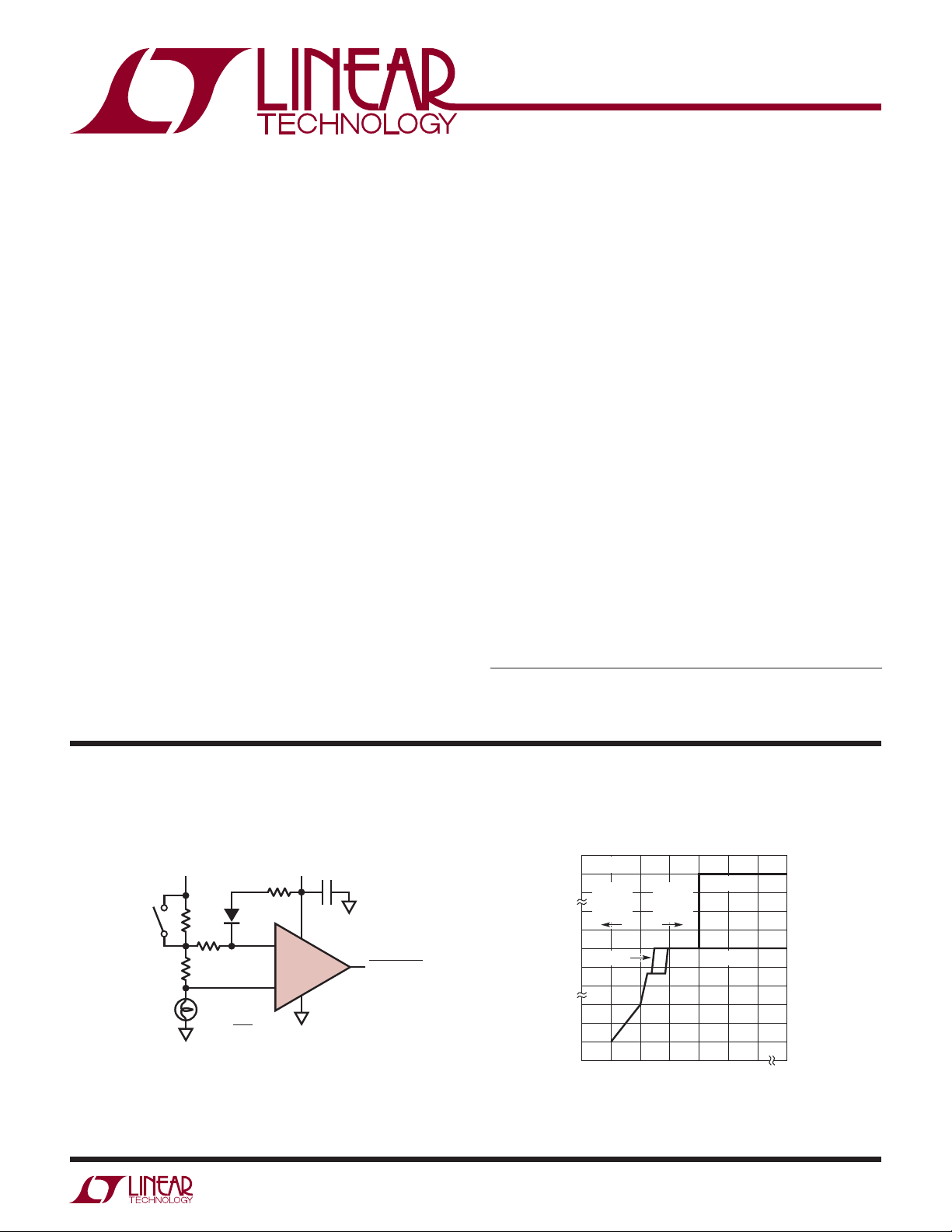
Lamp Monitor
3V
1M
5
4
–
LT1716 LAMP GOOD
3
+
2
1716 TA01
LAMP
ON/OFF
0.15Ω
0.25A TO 2.5A
5V TO 44V
100k
R
S
1W
5k
RS ≥
CMPD6001
0.04
I
L
0.1μF
Input Bias Current vs Input Bias Voltage
12μ
VS = 5V, 0V
8μ
INPUT
4μ
BELOW
6n
SUPPLY
3n
0
(A)
1
–
+IN = 2V +IN = 2V
B
–3n
I
–6n
–100m
–0.5m
–1m
–1.5m
–5 0 5 10 15 20 45
–10
INPUT
ABOVE
SUPPLY
V
+IN = 10V
–
(V)
IN
1716 TA02
1716fa
1
Page 2
LT1716
PIN CONFIGURATION ABSOLUTE MAXIMUM RATINGS
(Note 1)
Supply Voltage (V+ to V–) .........................................44V
Differential Input Voltage ..........................................44V
Input Voltage .....................................................44V, –5V
Output Short-Circuit Duration (Note 2) ............ Indefi nite
Operating Temperature Range (Note 3)
LT1716C/LT1716I ................................ –40°C to 85°C
LT1716H ............................................ –40°C to 125°C
OUT
+IN
TOP VIEW
1
–
2
V
3
5-LEAD PLASTIC TSOT-23
T
= 150°C, θJA = 250°C/W
JMAX
–
+
S5 PACKAGE
54V
+
–IN
Specifi ed Temperature Range (Note 4)
LT1716C/LT1716I ................................ –40°C to 85°C
LT1716H ............................................ –40°C to 125°C
Maximum Junction Temperature .......................... 150°C
Storage Temperature Range ..................–65°C to 150°C
Lead Temperature (Soldering, 10 sec)...................300°C
ORDER INFORMATION
LEAD FREE FINISH TAPE AND REEL PART MARKING* PACKAGE DESCRIPTION SPECIFIED TEMPERATURE RANGE
LT1716CS5#PBF LT1716CS5#TRPBF LTYD 5-Lead Plastic TSOT-23 –40°C to 85°C
LT1716IS5#PBF LT1716IS5#TRPBF LTYD 5-Lead Plastic TSOT-23 –40°C to 85°C
LT1716HS5#PBF LT1716HS5#TRPBF LTYD 5-Lead Plastic TSOT-23 –40°C to 125°C
Consult LTC Marketing for parts specifi ed with wider operating temperature ranges. *The temperature grade is identifi ed by a label on the shipping container.
Consult LTC Marketing for information on non-standard lead based fi nish parts.
For more information on lead free part marking, go to:
For more information on tape and reel specifi cations, go to:
http://www.linear.com/leadfree/
http://www.linear.com/tapeandreel/
ELECTRICAL CHARACTERISTICS
The l denotes the specifi cations which apply over the full operating
temperature range of –40°C ≤ TA ≤ 85°C, otherwise specifi cations are at TA = 25°C. Single supply operation V+ = 5V, V– = 0V;
VCM = V+/2 unless otherwise noted. (Note 4)
LTC1716C/LT1716I
SYMBOL PARAMETER CONDITIONS
V
OS
I
OS
I
B
CMRR Common Mode Rejection Ratio 0.5V ≤ V
Input Offset Voltage 0.5V < VCM < (VCC – 1V)
Input Offset Voltage Drift (Note 5) 0°C < T
Input Offset Current VCM = V+/2
Input Bias Current VCM = V+/2
Input Voltage Range (Note 7)
0°C < T
< 70°C
A
–40°C < T
–40°C < T
V
CM
VCM = 44V
+
V
V
CM
V
CM
V
CM
0.5V ≤ V
< 85°C
A
< 70°C
A
< 85°C
A
= 0V
= 0V, VCM = 44V
= 0V
= 44V
= –5V
< (V+ – 1V)
CM
< 44V (Note 6)
CM
l
l
l
l
l
l
l
l
l
l
l
l
0.5 44 V
l
89
l
81
300 1600
2
2
315
20
35
2
3
6
1
110
110
2100
2500
1.3
0.9
50
75
13
9
1.4
2
UNITSMIN TYP MAX
μV
μV
μV
μV/°C
μV/°C
nA
μA
μA
nA
nA
nA
μA
μA
mA
dB
dB
1716fa
Page 3
LT1716
ELECTRICAL CHARACTERISTICS
The l denotes the specifi cations which apply over the full operating
temperature range of –40°C ≤ T
VCM = V+/2 unless otherwise noted. (Note 4)
SYMBOL PARAMETER CONDITIONS
PSRR Power Supply Rejection Ratio V
Minimum Operating Supply Voltage
A
VOL
I
S
–
I
SC
+
I
SC
V
OL
V
OH
Large-Signal Voltage Gain RL = 1k; 1V < V
Supply Current V+ = 3V, RL = Open, VO = High
Output Sink Current (Note 2) V
Output Source Current V
Output Voltage Swing Low
(Referred to V
Output Voltage Swing High
(Referred to V
Leakage Current V
Propagation Delay V
≤ 85°C, otherwise specifi cations are at TA = 25°C. Single supply operation V+ = 5V, V– = 0V;
A
LTC1716C/LT1716I
–
= 0V, VCM = 1.5V; 2.7V < V+ < 36V
< 4V
OUT
l
95 110 dB
l
200
l
100
2.4 2.7 V
500 V/mV
35 50
l
+
V
= 5V, RL = Open, VO = High
l
+
V
= 12V, RL = Open, VO = High
OVERDRIVE
OVERDRIVE
I
–
)
+
)
SINK
I
SINK
I
SINK
I
SINK
I
SOURCE
I
SOURCE
OUT
OVERDRIVE
> 30mV
= 5mV, V
= 0mA, V
= 0.1mA
= 1mA
= 5mA
= 0μA, V
= 10μA
= 40V, V
> 100mV, R
OUT
OVERDRIVE
OVERDRIVE
OVERDRIVE
= 1V
= –10mV
= 10mV
> 100mV
= 10k 3 5.5 μs
LOAD
l
l
10 20 mA
l
60 85 μA
l
l
l
l
l
l
l
35 55
40 60
20
75
200
550
30
130
0.5 2 μA
65
75
85
35
110
300
900
55
185
UNITSMIN TYP MAX
V/mV
μA
μA
μA
μA
μA
μA
mV
mV
mV
mV
mV
mV
The l denotes the specifi cations which apply over the full operating temperature range of –40°C ≤ TA ≤ 85°C, otherwise specifi cations
are at TA = 25°C. Split supply operation VS = ±15V, VCM = 0V unless otherwise noted. (Note 4)
LT1716C/LT1716I
SYMBOL PARAMETER CONDITIONS
V
OS
Input Offset Voltage –14.5V < VCM < 14V
0°C < T
< 70°C
A
–40°C < T
< 85°C
A
Input Offset Voltage Drift (Note 5) 0°C < TA < 70°C
–40°C < T
I
OS
Input Offset Current VCM = 0V
< 85°C
A
VCM = 29V
V
= –15V
CM
I
B
Input Bias Current VCM = 0V
= 29V
V
CM
V
= –15V
CM
V
= –20V
CM
Input Voltage Range (Note 7)
CMRR Common Mode Rejection Ratio –14.5V < V
–14.5V < V
PSRR Power Supply Rejection Ratio V
S
CM
CM
= ±1.35V to ±22V
Minimum Operating Supply Voltage
A
VOL
I
S
–
I
SC
+
I
SC
Large-Signal Voltage Gain RL = 6k; –14V < V
Supply Current VS = ±15V, RL = Open, VO = High
Output Sink Current (Note 2) V
Output Source Current V
OVERDRIVE
OVERDRIVE
> 30mV
= 5mV, V
< 14V
< 29V (Note 6)
< 14V
OUT
= –14V
OUT
l
l
l
l
l
l
l
2
2
315
30
l
l
l
l
l
–14.5 14 V
l
92
l
81
l
90 110 dB
l
500
l
400
l
l
10 20 mA
l
70 105 μA
50
6
3
1
110
98
2.4 2.7 V
1000 V/mV
40 95 μA
2000
2400
0.9
1.3
60
100
9
13
1.4
300 1500
UNITSMIN TYP MAX
μV
μV
μV
μV/°C
μV/°C
nA
μA
μA
nA
nA
μA
μA
mA
dB
dB
V/mV
1716fa
3
Page 4
LT1716
The l denotes the specifi cations which apply over the full operating
ELECTRICAL CHARACTERISTICS
temperature range of –40°C ≤ T
unless otherwise noted. (Note 4)
SYMBOL PARAMETER CONDITIONS
V
OL
Output Voltage Swing Low
(Referred to V
V
OH
Output Voltage Swing High
(Referred to V
Leakage Current V
Propagation Delay V
The l denotes the specifi cations which apply over the full operating temperature range of –40°C < TA < 125°C, otherwise specifi cations
are at TA = 25°C. Single supply operation V+ = 5V, V– = 0V; VCM = VCC/2 unless otherwise noted. (Note 4)
SYMBOL PARAMETER CONDITIONS
V
OS
I
OS
I
B
CMRR Common Mode Rejection Ratio 0.5V < V
PSRR Power Supply Rejection Ratio V
A
VOL
I
S
–
I
SC
+
I
SC
V
OL
V
Output Voltage Swing High
OH
Input Offset Voltage 0.5V < VCM < (VCC – 1V)
Input Offset Voltage Drift (Note 5)
Input Offset Current VCM = V+/2
Input Bias Current VCM = V+/2
Input Voltage Range (Note 7) 0.5 44 V
Minimum Operating Supply Voltage
Large-Signal Voltage Gain RL = 1k, 1V < V
Supply Current per Amplifi er V+ = 3V, RL = Open, VO = High
Output Sink Current (Note 2) V
Output Source Current V
Output Voltage Swing Low
(Referred to V
(Referred to V
Leakage Current V
Propagation Delay V
≤ 85°C, otherwise specifi cations are at TA = 25°C. Split supply operation VS = ±15V, VCM = 0V
A
LT1716C/LT1716I
= 0mA, V
I
–
)
+
)
SINK
I
= 0.1mA
SINK
I
= 1mA
SINK
I
= 5mA
SINK
I
SOURCE
I
SOURCE
= 25V, V
OUT
OVERDRIVE
OVERDRIVE
= 0μA, V
= 10μA
OVERDRIVE
> 100mV, R
= –10mV
OVERDRIVE
> 100mV
LOAD
= 10mV
= 10k 5.5 9 μs
l
l
l
l
l
l
l
20
75
200
550
45
140
0.6 2 μA
LT1716H
300 1600
l
V
V
CM
CM
= 0V
= 44V
l
l
l
l
2μV/°C
3 220
20 50
l
+
= 0V, VCM = 44V
V
V
= 0V
CM
V
= 44V
CM
V
= –5V
CM
< (V+ – 1V)
CM
0.5V < V
–
R
L
< 44V (Note 6)
CM
= 0V, VCM = 1.5V, 2.7V < V+ < 36V
< 4V
OUT
= 6k
l
l
l
l
75
l
72
l
85 110 dB
l
200
l
20
2
3
6
1
110
110
2.4 2.7 V
500 V/mV
35 50
l
+
= 5V, RL = Open, VO = High
V
+
= 12V, RL = Open, VO = High
V
OVERDRIVE
OVERDRIVE
I
–
)
+
)
SINK
I
SINK
I
SINK
I
SINK
I
SOURCE
I
SOURCE
OUT
OVERDRIVE
> 30mV
= 5mV, V
= 0mA, V
= 0.1mA
= 1mA
= 5mA
= 0μA, V
= 10μA
= 40V, V
> 100mV, R
OUT
OVERDRIVE
OVERDRIVE
OVERDRIVE
= 1V
= –10mV
= –10mV
> 100mV
= 10k 6 9 μs
LOAD
l
l
l
510 mA
l
60 110 μA
l
l
l
l
l
l
l
35 55
40 60
20
75
200
550
50
130
1.7 5 μA
35
110
300
900
75
210
2900
1.3
0.9
900
25
14
1.4
70
75
85
60
170
480
1200
110
220
UNITSMIN TYP MAX
mV
mV
mV
mV
mV
mV
UNITSMIN TYP MAX
μV
μV
nA
μA
μA
nA
nA
nA
μA
μA
mA
dB
dB
V/mV
μA
μA
μA
μA
μA
μA
mV
mV
mV
mV
mV
mV
1716fa
4
Page 5

LT1716
The l denotes the specifi cations which apply over the full operating
ELECTRICAL CHARACTERISTICS
temperature range of –40°C < T
unless otherwise noted. (Note 4)
SYMBOL PARAMETER CONDITIONS
V
OS
I
OS
I
B
CMRR Common Mode Rejection Ratio –14.5V < V
PSRR Power Supply Rejection Ratio VS = ±1.35V to ±22V
A
VOL
I
S
–
I
SC
+
I
SC
V
OL
V
OH
Input Offset Voltage –14.5V < VCM < 14V
Input Offset Voltage Drift (Note 5)
Input Offset Current VCM = 0V
Input Bias Current VCM = 0V
Input Voltage Range (Note 7)
Minimum Operating Supply Voltage
Large-Signal Voltage Gain RL = 6k; –14V < V
Supply Current VS = ±15V, RL = Open, VO = High 40 95 μA
Output Sink Current (Note 2) V
Output Source Current V
Output Voltage Swing Low
(Referred to V
Output Voltage Swing High
(Referred to V
Leakage Current V
Propagation Delay V
< 125°C, otherwise specifi cations are at TA = 25°C. Split supply operation VS = ±15V, VCM = 0V
A
LT1716H
300 1500
l
V
CM
V
CM
= 29V
= –15V
l
l
l
l
2 μV/°C
3 280
30
l
VCM = 29V
V
= –15V
CM
V
= –20V
CM
< 14V
–14.5V < V
R
L
OVERDRIVE
OVERDRIVE
I
–
)
+
)
SINK
I
SINK
I
SINK
I
SINK
I
SOURCE
I
SOURCE
OUT
OVERDRIVE
CM
< 29V (Note 6)
CM
= 6k; –13V < V
> 30mV
= 5mV, V
= 0mA, V
OVERDRIVE
= 0.1mA
= 1mA
= 5mA
= 0μA, V
= 10μA
= 25V, V
OVERDRIVE
> 100mV, R
< 14V
OUT
< 13V
OUT
= –14V
OUT
= –10mV
OVERDRIVE
> 100mV
LOAD
= 10mV
= 10k 5.5 10 μs
l
l
l
l
–14.5 14 V
l
85
l
70
l
80 110 dB
l
500501000 V/mV
l
l
510 mA
l
70 155 μA
l
l
l
l
l
l
l
50
6
3
1
110
93
2.4 2.7 V
20
75
200
550
45
140
1.5 5 μA
2900
0.9
1.3
60
1400
20
30
1.4
70
170
480
1200
120
250
UNITSMIN TYP MAX
μV
μV
nA
μA
μA
nA
nA
μA
μA
mA
dB
dB
V/mV
mV
mV
mV
mV
mV
mV
Note 1: Stresses beyond those listed under Absolute Maximum Ratings
may cause permanent damage to the device. Exposure to any Absolute
Maximum Rating condition for extended periods may affect device
reliability and lifetime.
Note 2: A heat sink may be required to keep the junction temperature
below absolute maximum.
Note 3: The LT1716C/LT1716I are guaranteed functional over the operating
temperature range of –40°C to 85°C. The LT1716H is guaranteed
functional over the operating temperature range of –40°C to 125°C.
Note 4: The LT1716C is guaranteed to meet specifi ed performance from
0°C to 70°C. The LT1716C is designed, characterized and expected to meet
performance from –40°C to 85° but is not tested or QA sampled at the
temperatures. The LT1716I is guaranteed to meet specifi ed performance
from –40°C to 85°C. The LT1716H is guaranteed to meet specifi ed
performance from –40°C to 125°C.
Note 5: This parameter is not 100% tested.
Note 6: Typical input offset voltage of 500μV at V
maximum input offset voltage of 4mV at V
CM
= 44V above V– and a
CM
= 44V above V–.
Note 7: If one input is within this input range, the other input can go 5V
below V– and the output will be valid.
1716fa
5
Page 6

LT1716
TYPICAL PERFORMANCE CHARACTERISTICS
Input Bias Current
vs Common Mode Voltage
10
VS = ±15V
8
25°C
85°C
–55°C
INPUTS
EXCEED SUPPLY
(μA)
BIAS
I
6
4
2
0
–2
0
125°C
5 10 15 20 25 30
VCM (V)
Output Low Voltage
vs Sink Current
2.0
1.6
1.2
0.8
0.4
OUTPUT VOLTAGE (RELATIVE TO GND) (V)
0
VOL AT 125°C
VOL AT 85°C
VOL AT 25°C
VOL AT –55°C
0
2 4 6 8 10 12 14 16 18 20
LOADING SINK CURRENT (mA)
125°C
1716 G01
V+ = 5V
–
= 0V
V
1716 G04
Input Bias Current
vs Temperature
1.0000
0.1000
0.0100
0.0010
0.0000
INPUT BIAS CURRENT (μA)
–0.0010
–0.0100
CURRENT
OUT OF PIN
–50
–25 25
V+ = 15V
–
= –15V
V
= 0V
V
CM
CURRENT
OUT OF PIN
050
TEMPERATURE (°C)
Output High Voltage
vs Source Current
5.0
) (V)
+
4.9
4.8
4.7
4.6
OUTPUT HIGH VOLTAGE (RELATIVE TO V
4.5
0
5 10 15 20 25 30 35 40 45 50
VOH AT –55°C
VOH AT 85°C, 125°C
VOH AT 25°C
LOADING SOURCE CURRENT (μA)
Input Bias Current
vs Differential Input Voltage
1
0
V+ = 5V
–
= 0V
V
= 2.5V
V
CM
100
75
125
150
1716 G02
–1
CURRENT (nA)
–2
BIAS
I
–3
–4
–0.2
–0.15 –0.1
DIFFERENTIAL INPUT VOLTAGE (V)
V+ = 15V
–
= –15V
V
–IN +IN
TRANSITION
REGION
0
–0.05 0.05 0.2
0.1 0.15
1716 G03
Input Bias Current with Inputs
Driven Above the Supply
(μA)
BIAS
I
10
V+ = 5V
–
= 0V
V
8
6
4
2
0
–2
0
51015 20 25 30 35 40 45 50
125°C
85°C
25°C
INPUTS
EXCEED SUPPLY
VCM (V)
–55°C
1716 G06
V+ = 5V
–
= 0V
V
1716 G05
Input Bias Current with Inputs
Driven Below the Supply Supply Current vs Temperature
–200
–400
(μA)
–600
BIAS
I
–800
–1000
–1200
200
V+ = 2.7V TO 44V
–
= 0V
V
0
–55°C < TA < 125°C
–5
–4 –3 –2 –1 0
VCM (V)
1716 G07
100
V+ = 5V
–
90
= 0V
V
80
70
60
50
40
30
SUPPLY CURRENT (μA)
20
10
0
–50
–25 25
OUTPUT LOW
0
TEMPERATURE (°C)
OUTPUT HIGH
6
Positive Supply Current
vs Output Sinking Current
1000
TA = 25°C
100
POSITIVE SUPPLY CURRENT (μA)
125
50
100
75
150
1716 G08
10
0.1
VS = ±15V
1 10 100
OUTPUT SINK CURRENT (mA)
VS = 5V
1716 G09
1716fa
Page 7

TYPICAL PERFORMANCE CHARACTERISTICS
LT1716
Output Leakage Current
vs Output Voltage Reverse Supply Current
500
V+ = 5V
–
= 0V
V
= 25°C
T
A
450
400
350
300
OUTPUT LEAKAGE CURRENT (nA)
250
5
10 15 20 25 30 35 40 45
OUTPUT VOLTAGE (V)
Output Sinking Current
vs Total Supply Voltage
30
OUTPUT SHORTED TO V
TA = 25°C
25
20
15
10
OUTPUT SINKING LIMIT (mA)
5
0
1
TOTAL SUPPLY VOLTAGE (V)
10 100
1716 G10
+
1716 G12
0.6
TA = 25°C
0.5
0.4
0.3
0.2
REVERSE CURRENT (mA)
0.1
0
0
5 10 15 20 25
REVERSE VOLTAGE (V)
Total Switching Time
vs Temperature
100
VS = ±15V
RISE
10
VS = ±2.5V
–50 –25
FALL
0
25 75
TEMPERATURE (°C)
TOTAL SWITCHING TIME (μs)
1
RL = 10k
= 90% V
V
OUT
= 10% V
V
OUT
= 100mV
V
STEP
V
OVERDRIVE
VS = ±15V
FALL
VS = ±2.5V
RISE
50
FINAL
FINAL
= 10mV
100
1716 G27
(RISE)
(FALL)
125
1716 G13
30
25
20
15
10
OUTPUT CURRENT LIMIT (mA)
5
0
–50
100
10
TOTAL SWITCHING TIME (μs)
150
1
Output Sinking Current Limit
vs Temperature
OUTPUT SHORTED TO V
VS = ±15V
050
–25 25
TEMPERATURE (°C)
+
VS = 5V
75
100
Total Switching Time
vs Overdrive
RL = 10k
= 90% V
V
OUT
V
OUT
V
STEP
= 25°C
T
A
±2.5V
FALL TIME
±2.5V
RISE TIME
20 100
10
0
40
50
30
OVERDRIVE (mV)
= 10% V
= 100mV
FALL TIME
RISE TIME
FINAL
FINAL
±15V
±15V
807060
125
1716 G11
(RISE)
(FALL)
90
1716 G14
150
Total Switching Time
vs Total Supply Voltage
100
RL = 10k
= 90% V
V
OUT
V
OUT
V
CM
V
STEP
V
OVERDRIVE
10
TOTAL SWITCHING TIME (μs)
1
0
FINAL
= 10% V
FINAL
= 1/2 V
TOTALSUPPLY
= 100mV
= 10mV
10
TOTAL SUPPLY VOLTAGE (V)
(RISE)
(FALL)
FALL
RISE
20
Total Switching Time
vs Pull-Up Resistor Response Time
100
V
= 90% V
OUT
V
STEP
V
OVERDRIVE
= 25°C
T
A
10
TOTAL SWITCHING TIME (μs)
30
40
1716 G15
1
1 10
FINAL
= 100mV
= 10mV
VS = ±15V
RISE
VS = ±2.5V
RISE
100 1000 10000
PULL-UP RESISTOR (k)
1716 G16
30V
+
V
IN
26V
5V
R
= 100k
L
V
OUT
RL = 10k
0V
= 5V, 0V
S
= 10mV
V
OD
= 10k, 100k, OPEN
R
L
+
= 26V TO 30V
V
IN
–
= 29.99V
V
IN
= OPEN
R
L
TIME (μs)V
1716 G17
1716fa
7
Page 8
LT1716
TYPICAL PERFORMANCE CHARACTERISTICS
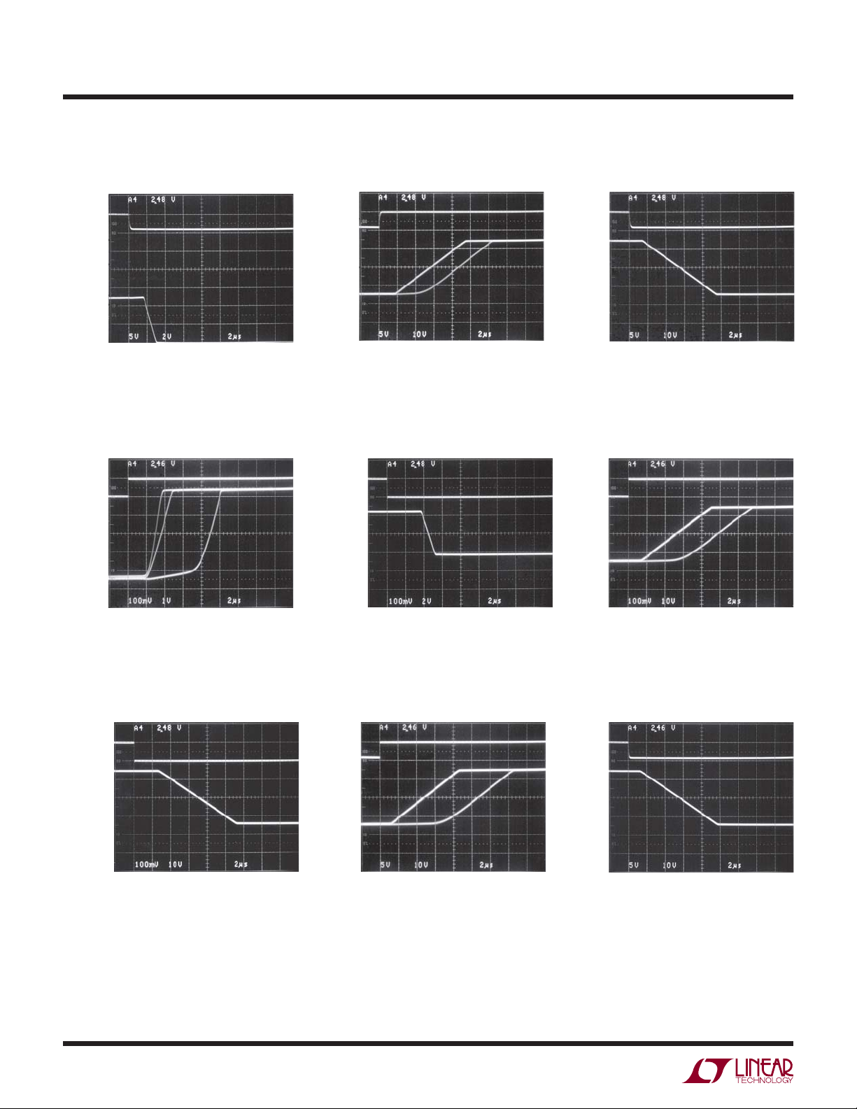
Response Time Response Time Response Time
30V
+
V
IN
26V
5V
V
OUT
0V
= 5V, 0V
S
V
= 10mV
OD
= 10k, 100k, OPEN
R
L
+
= 30V TO 26V
V
IN
–
= 26.01V
V
IN
TIME (μs)V
Response Time Response Time Response Time
2.5V V
+
V
IN
2.4V
RL = 10k RL = 100k
R
= OPEN
L
= ±15V
S
= 10mV
V
OD
= 10k, 100k, OPEN
R
L
+
= 2.4V TO 2.5V
V
IN
–
= 2.49V
V
IN
TIME (μs)V
1716 G18
1716 G21
25V
+
V
IN
21V
15V
V
OUT
RL = 10k, 100k
R
L
= OPEN
–15V
= ±15V
S
= 10mV
V
OD
= 10k, 100k, OPEN
R
L
+
= 21V TO 25V
V
IN
–
= 24.99V
V
IN
2.6V
+
OUT
V
IN
5V
2.5V
TIME (μs)V
1716 G19
5V
V
OUT
0V
V
IN
V
OUT
V
IN
–100mV
V
OUT
+
–15V
+
–15V
25V
21V
15V
0V
15V
= ±15V
S
= 10mV
V
OD
= 10k, 100k, OPEN
R
L
+
= 25V TO 21V
V
IN
–
= 21.01V
V
IN
RL = 10k, 100k
TIME (μs)V
= OPEN
R
L
1716 G20
0V
= 5V
S
= 10mV
V
OD
= 10k, 100k, OPEN
R
L
+
= 2.6V TO 2.5V
V
IN
–
= 2.51V
V
IN
TIME (μs)V
1716 G22
= ±15V
S
= 10mV
V
OD
= 10k, 100k, OPEN
R
L
+
= –100mV TO 0V
V
IN
–
= –10mV
V
IN
TIME (μs)V
1716 G23
V
IN
V
8
Response Time Below V
100mV
+
OUT
15V
–15V
0V
S
V
OD
R
L
V
IN
V
IN
= ±15V
= 10mV
= 10k, 100k, OPEN
+
= 110mV TO 0mV
–
= 10mV
TIME (μs)V
V
1716 G24
IN
V
–14.9V
+
OUT
–19V
15V
–15V
S
R
L
V
IN
V
IN
–
Fault (Rising) Below V
S
RL = 10k, 100k
= ±15V
= 10k, 100k, OPEN
+
= –19V TO –14.9V
–
= –15V
–
Fault (Falling)
S
–14.9V
+
V
IN
–19V
15V
V
= OPEN
R
L
OUT
–15V
TIME (μs)V
1716 G25
= ±15V
S
= 10k, 100k, OPEN
R
L
+
= –14.9V TO –19V
V
IN
–
= –15V
V
IN
TIME (μs)V
1716 G26
1716fa
Page 9

APPLICATIONS INFORMATION
LT1716
The LT1716 comparator features low power operation
with exceptional input precision with rail-to-rail input and
output swing. The comparator operates fl awlessly even
when the inputs are pulled over the positive rail or below
the negative rail.
Supply Voltage
The LT1716 operates from 2.7V to 44V. The comparator
+
can be shut down by removing V
. In this condition, the
input bias current is typically less than 3nA, even if the
inputs are 44V above the negative supply. The LT1716 is
protected against reverse battery voltages of up to 20V.
The reverse battery current is resistive as shown in the
Reverse Supply Current graph.
Inputs
The comparator inputs can swing from 0.5V above to 44V
–
above V
can be forced up to 5V below V
. If one input is within this range, the other input
–
without phase reversal
occuring at the output.
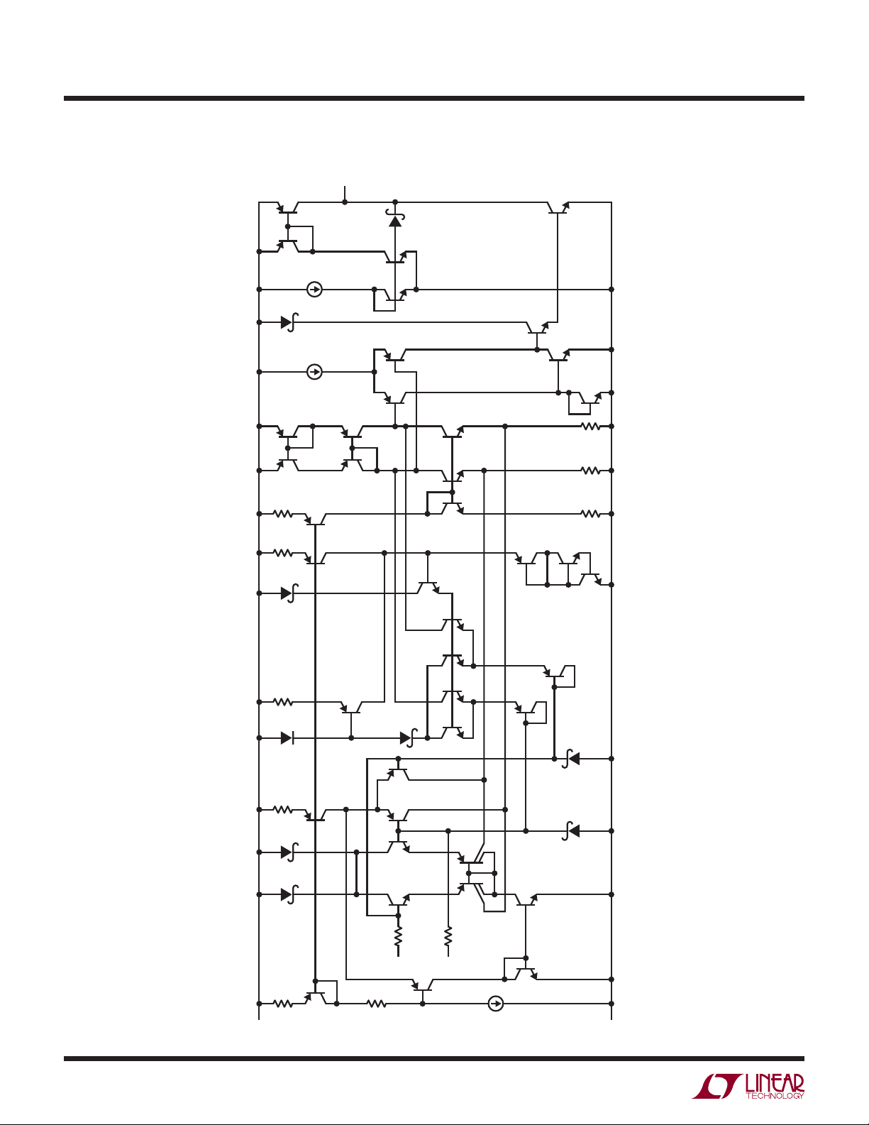
The LT1716 has three stages—NPN, PNP and common
base (see Simplifi ed Schematic)—resulting in three
distinct operating regions and two transition regions as
shown in the Input Bias Current vs Common Mode typical
performance curve.
+
For input voltages about 0.8V or more below V
, the PNP
input stage is active and the input bias current is typically
–4nA. The PNP differential input stage will have bias current that fl ows out of the device. With a differential input
voltage of even just 100mV or so, there will be zero bias
current into the higher of the two inputs, while the current
fl owing out of the lower input will be twice the measured
bias current.
+
When the input voltage is about 0.5V or less from V
, the
NPN state is operating and the input bias current is typically
10nA. Increases in temperature will cause the voltage at
which operation switches from the PNP stage to the NPN
+
stage to move towards V
. The input offset voltage of the
NPN stage is untrimmed and is typically 500μV.
A Schottky diode in the collector of each NPN transistor
of the NPN input stage allows the LT1716 to operate with
+
either or both of its inputs above V
+
, the NPN transistor is fully saturated and the input bias
V
. At about 0.3V above
current is typically 4μA at room temperature. The input
offset voltage is typically 500μV when operating above
+
. The LT1716 will operate with its input 44V above V–,
V
regardless of V
+
.
The transition to the negative common mode input stage
–
occurs at 0.3V above V
stage is active. When the inputs are 0.3V below V
. Above this trip point the PNP
–
, the
common base input stage is active in addition to the PNP
stage. The input bias current out of each input becomes
/5kΩ. The LT1716 is designed to operate when either
V
IN
input falls below the negative supply. Internal resistors
protect the inputs for faults below the negative supply of
up to 5V without phase reversal. The built-in 5k resistor
limits the current at each input to 1mA at 5V below the
negative supply. External matched input resistors can
be added for increased voltage fault operation below the
negative supply but the maximum input current should
be kept under 1mA.
Input Protection
The inverting and noninverting input pins of the LT1716
have on-chip protection. ESD protection is provided to
prevent damage during handling. The input transistors
have voltage clamping and limiting resistors to protect
–
against excursions as much as 5V below V
. There are
no clamping diodes between the inputs and the maximum
differential input voltage is 44V.
Output
The output stage of the LT1716 can drive loads connected
to a supply more positive than the device, the same as
comparators with open collector output stages. The
–
output of the LT1716 can be pulled up to 44V above V
+
regardless of V
.
,
1716fa
9
Page 10
LT1716
SIMPLIFIED SCHEMATIC
Q29
Q28D8
OUT
Q30
D7
Q26 Q27
Q38
Q37
1716 SS
Q31 Q32
Q23
Q22
R7
D6D2D1
R8 R6
Q12 Q13
R5
Q24
Q25
Q14
Q53
D5
Q2
Q9
Q8
Q10
Q33
Q39
Q18
Q17Q16Q15
Q61
Q6BA
Q36
R9 R10 R11
Q34
Q35
Q62
D4D3
10
Q3 Q4 Q1
5k
R1
R4
Q11
30k
CC
V
R3
60k
R2
–
IN
Q7
B
Q5
5k
+
IN
Q20
A
Q21
3μA
EE
V
1716fa
Page 11

PACKAGE DESCRIPTION
LT1716
S5 Package
5-Lead Plastic TSOT-23
(Reference LTC DWG # 05-08-1635)
0.62
MAX
3.85 MAX
0.20 BSC
DATUM ‘A’
NOTE:
1. DIMENSIONS ARE IN MILLIMETERS
2. DRAWING NOT TO SCALE
3. DIMENSIONS ARE INCLUSIVE OF PLATING
4. DIMENSIONS ARE EXCLUSIVE OF MOLD FLASH AND METAL BURR
5. MOLD FLASH SHALL NOT EXCEED 0.254mm
6. JEDEC PACKAGE REFERENCE IS MO-193
2.62 REF
RECOMMENDED SOLDER PAD LAYOUT
PER IPC CALCULATOR
0.30 – 0.50 REF
0.95
REF
1.22 REF
1.4 MIN
0.09 – 0.20
(NOTE 3)
2.80 BSC
1.50 – 1.75
(NOTE 4)
1.00 MAX
PIN ONE
0.95 BSC
0.80 – 0.90
2.90 BSC
(NOTE 4)
0.30 – 0.45 TYP
5 PLCS (NOTE 3)
0.01 – 0.10
1.90 BSC
S5 TSOT-23 0302
Information furnished by Linear Technology Corporation is believed to be accurate and reliable.
However, no responsibility is assumed for its use. Linear Technology Corporation makes no representation that the interconnection of its circuits as described herein will not infringe on existing patent rights.
1716fa
11
Page 12
LT1716
TYPICAL APPLICATIONS
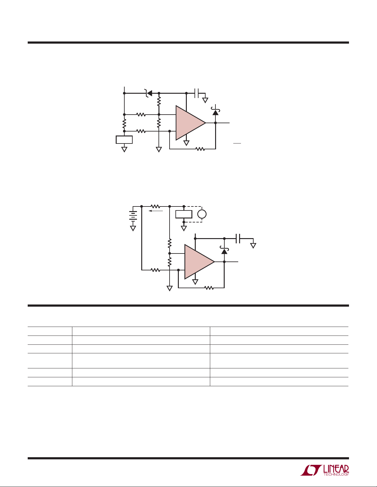
Overcurrent Flag
4.5V TO 44V
R
S
LOAD
3V TO 44V
LT1634-1.25
11.8k
1%
10.7k
1%
CHARGE
CURRENT
681Ω
0.1μF
113k
1%
10M
1%
5
4
–
LT1716 OVERCURRENT
3
+
1
2
10M
1%
Charge/Discharge Indicator
0.1Ω
+
CHARGER
–
3V
5
–
LT1716 CHARGE
+
2
1M
1%
1%
1%
1M
LOAD V
681Ω
1%
4
3
3V
CMPD6263
I
1
MAX
0.1
=
R
S
0.1μF
CMPD6263
1716 TA03
1716 TA04
RELATED PARTS
PART NUMBER DESCRIPTION COMMENTS
LTC1442 Dual Micropower Comparator and 1% Reference 1.182V ±1% Reference, ±10mV
LTC1540 Nanopower Comparator and 1% Reference 1.182V ±1% Reference, ±10mV
LT1634 Micropower Precision Shunt Reference 0.05%, 10μA, 10ppm/°C Max Drift, 1.25V, 2.5V, 4.096V, 5V,
MSOP, SO-8, TO-92 Packages
LTC1921 Dual –48V Telecom Supply Monitor Monitors Two Supplies and Fuses
LTC1998 Micropower Li-Ion Battery Monitor 1% Trip Point Adjustable from 2.5V to 3.25V
Linear Technology Corporation
12
1630 McCarthy Blvd., Milpitas, CA 95035-7417
(408) 432-1900 ● FAX: (408) 434-0507
●
www.linear.com
Input Offset
MAX
Input Offset
MAX
LT 0809 REV A • PRINTED IN USA
© LINEAR TECHNOLOGY CORPORATION 2002
1716fa
Page 13

 Loading...