

Lierda LSD1BT-STBLEPCB Product Manual
1
利尔达科技集团股份有限公司
LIERDA SCIENCE & TECHNOLOGY GROP CO.,LTD
LSD1BT-STBLEPCB
Product manual
Product Name:
BlueNRG-A Bluetooth module PCBA
P/N: LSD1BT-STBLEPCB
Document version: V4.0
2
Revision history
Product
Name
BlueNRG-A
Bluetooth module
PCBA
Product Type LSD1BT-STBLEPCB
Editor Qiumg Date 20170726
No. Revision record Modifier Auditor Versions Date
1 Initial release Liuzh V1.0 20161012
2 Liuzh V1.1 20161210
3 Add descriptions of
product information;
Modify partial data;
Add figure comments
Marco Qiu V2.0 20170726
4 The module power is
divided into BAT1 and
BAT2 in pin definition
Marco Qiu V3.0 20171225
5
Add FCC&CE
Information
Marco Qiu V4.0 20180108
6
Marco Qiu V5.0 20180118
3
Information
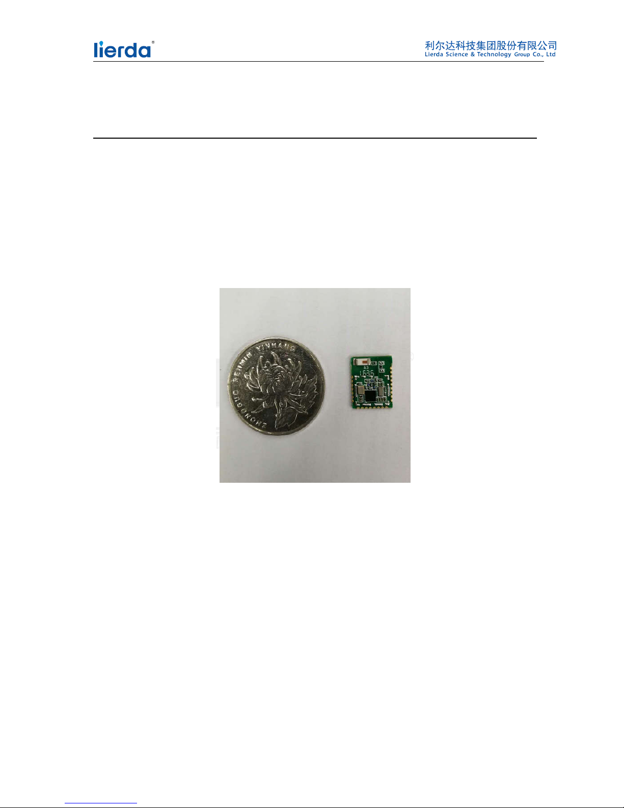
Part Number Description Package Size
LSD1BT-STBLEPCB
The PN is pure hardware without shield or any
firmware. Please contact us if there is other
requirements for second development of end users.
13mm*10mm*2.3mm
-- --
--
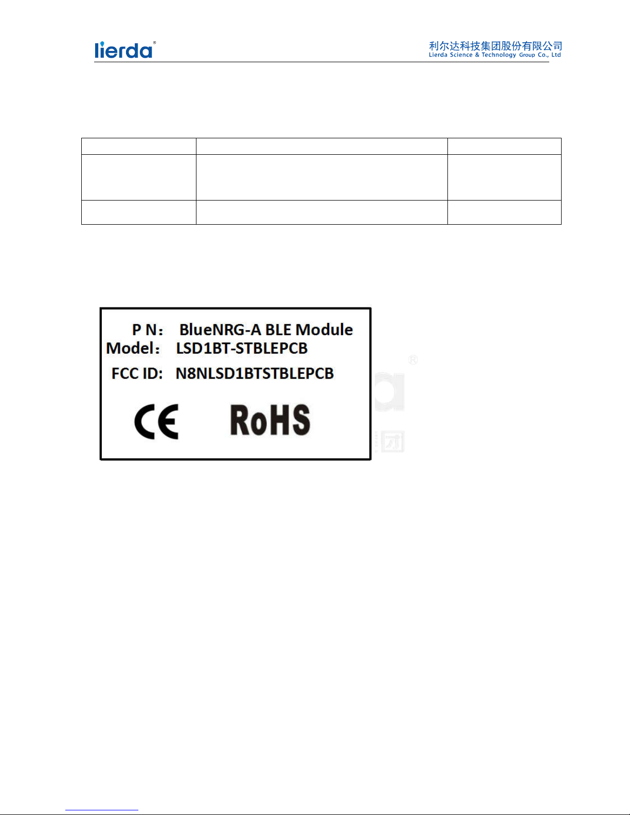
The Label
This device complies with Part 15 of the FCC Rules. Operation is subject to the
following two conditions: (1) this device may not cause harmful interference, and (2)
this device must accept any interference received, including interference that may
cause undesired operation.
4
Contents
1 Features .......................................................................................................................................................... 5
2 Specifications ................................................................................................................................................. 6
3 Hardware ........................................................................................................................................................ 7
3.1 Dimensions Diagram ........................................................................................................................... 7
3.2 Pin Description .................................................................................................................................... 8
4 Applications .................................................................................................................................................... 9
4.1 Application circuit ............................................................................................................................... 9
4.2 Precautions ........................................................................................................................................ 10
4.3 Download and Debug ........................................................................................................................ 10
4.4 Development board ........................................................................................................................... 10
4.5 Reference manual .............................................................................................................................. 10
5 Federal Communications Commission (FCC) Interference Statement ......................................................... 11
Note ................................................................................................................................................................. 12
 Loading...