

Page 1
Global LCD Panel Exchange Center
( ) Preliminary Specification
(
) Final Specification
www.panelook.com
LM240WU2
Liquid Crystal Display
Product Specification
SPECIFICATION
FOR
APPROVAL
BUYER
MODEL
APPROVED BY
/
/
APPLE
SIGNATURE
DATE
24.0” WUXGA TFT LCDTitle
LG.Philips LCD Co., Ltd.SUPPLIER
LM240WU2*MODEL
SLB1/SLB2/SLB3SUFFIX
*When you obtain standard approval,
please use the above model name without suffix
APPROVED BY
Hans Kim / G.Manager
REVIEWED BY
S.Y Park / Manager
SIGNATURE
DATE
PREPARED BY
/
Please return 1 copy for your confirmation with
your signature and comments.
Ver. 1.0 Jan. 01. 17. 2008
One step solution for LCD / PDP / OLED panel application: Datasheet, inventory and accessory!
Harry Kim / Engineer
MNT Products Engineering Dept.
LG. Philips LCD Co., Ltd
1/ 35
www.panelook.com
Page 2
Global LCD Panel Exchange Center
www.panelook.com
LM240WU2
Liquid Crystal Display
Product Specification
Contents
PageITEMNo
COVER
CONTENTS
RECORD OF REVISIONS
GENERAL DESCRIPTION1
ABSOLUTE MAXIMUM RATINGS2
ELECTRICAL SPECIFICATIONS3
ELECTRICAL CHARACTREISTICS3-1
INTERFACE CONNECTIONS3-2
SIGNAL TIMING SPECIFICATIONS3-3
SIGNAL TIMING WAVEFORMS3-4
COLOR INPUT DATA REFERNECE3-5
POWER SEQUENCE3-6
OPTICAL SFECIFICATIONS4
1
2
3
4
5
6
6
8
11
12
13
14
16
MECHANICAL CHARACTERISTICS5
RELIABLITY6
INTERNATIONAL STANDARDS7
SAFETY7-1
EMC7-2
PACKING8
DESIGNATION OF LOT MARK8-1
PACKING FORM8-2
PRECAUTIONS9
EDID DATA FOR LM240WU2-SLA110
22
25
26
26
26
27
27
27
28
30
Ver. 1.0 Jan. 01. 17. 2008
One step solution for LCD / PDP / OLED panel application: Datasheet, inventory and accessory!
2/ 35
www.panelook.com
Page 3
Global LCD Panel Exchange Center
www.panelook.com
LM240WU2
Liquid Crystal Display
Product Specification
RECORD OF REVISIONS
Revision
No
DescriptionPageRevision Date
Final Specification-Jan. 17. 20081.0
Ver. 1.0 Jan. 01. 17. 2008
One step solution for LCD / PDP / OLED panel application: Datasheet, inventory and accessory!
3/ 35
www.panelook.com
Page 4
Global LCD Panel Exchange Center
www.panelook.com
LM240WU2
Liquid Crystal Display
Product Specification
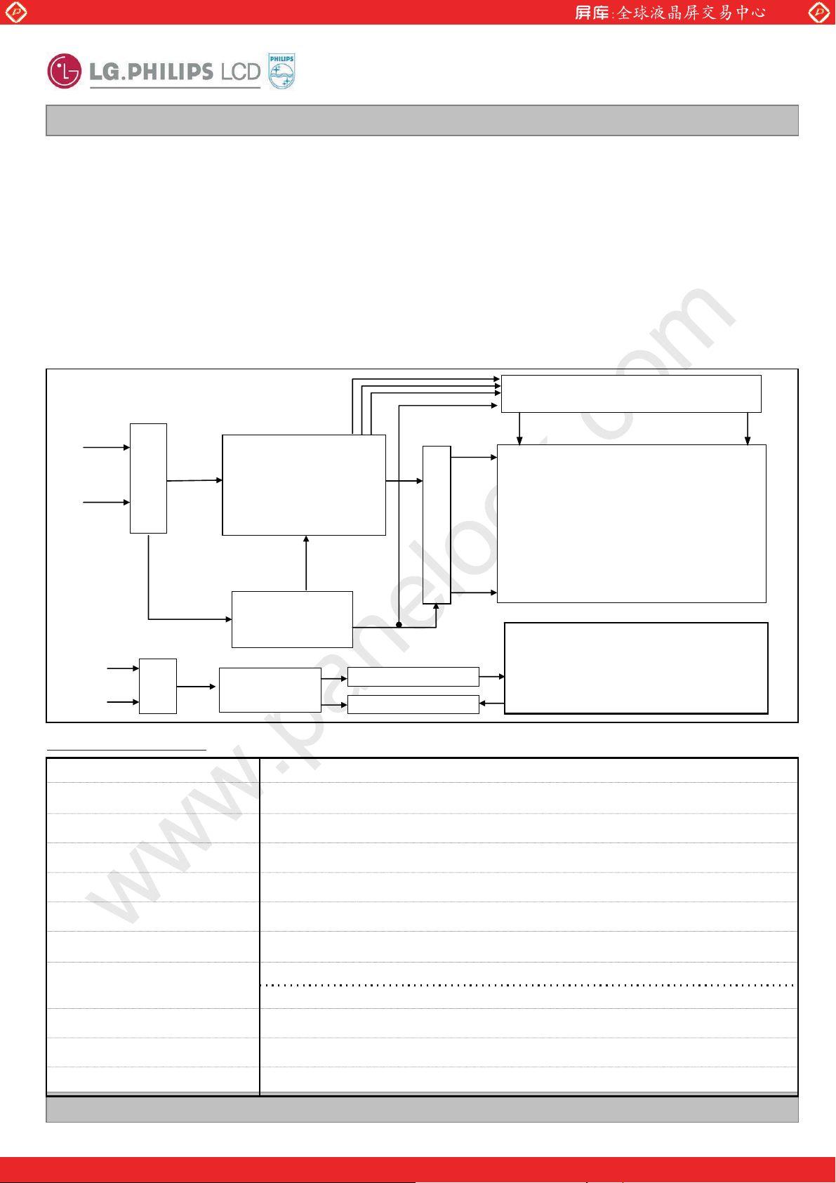
1. General Description
LM240WU2 is a Color Active Matrix Liquid Crystal Display with an integral Cold Cathode Fluorescent
Lamp(CCFL) backlight system. The matrix employs a-Si Thin Film Transistor as the active element.
It is a transmissive type display operating in the normally black mode. It has a 24inch diagonally measured
active display area with WUXGA resolution (1200 vertical by 1920 horizontal pixel array)
Each pixel is divided into Red, Green and Blue sub-pixels or dots which are arranged in vertical stripes.
Gray scale or the brightness of the sub-pixel color is determined with a 8-bit gray scale signal for each dot,
thus, presenting a palette of more than 16,7M(True) colors.
It has been designed to apply the 8Bit 2 port LVDS interface.
It is intended to support displays where high brightness, super wide viewing angle,
high color saturation, and high color are important.
LVDS
2port
CN1
(30pin)
+12.0V
+12.0V
+24.0V
GND
CN2
(14Pin)
General Features
RGB
Timing
Controller
Power Circuit
Block
Inverter
Block
24.0 inches(60.96cm) diagonalActive Screen Size
546.4(H) x 350.0(V) x 28.9(D) mm(Typ.)Outline Dimension
Gate Driver Circuit
2pin x 7CNs (High)
4pin x 1CNs (Low)
Source Driver Circuit
S1 S1920
G1
TFT - LCD Panel
(1920 Ý RGB Ý 1200 pixels)
G1200
Back light Assembly
(Direct Light Type_14CCFL)
0.270 mm x 0.270 mmPixel Pitch
1920 horiz. By 1200 vert. Pixels RGB stripes arrangementPixel Format
8-bit, 16,777,216 colorsColor Depth
400 cd/m
2
( 5 points Avg.)Luminance, White
View Angle Free (R/L 178(Typ.), U/D 178(Typ.))Viewing Angle(CR>10)
Total 71.95 Watt (Typ.) (5.95 Watt
@VLCD, 66 Watt @400cd) for SLB1/SLB3
Power Consumption
Total 70.92 Watt (Typ.) (4.92 Watt @VLCD, 66 Watt @400cd) for SLB2
2650g (typ.)Weight
Transmissive mode, normally blackDisplay Operating Mode
Hard coating(2H), Glare(Low Reflection treatment of the front polarizer)Surface Treatment
Ver. 1.0 Jan. 01. 17. 2008
One step solution for LCD / PDP / OLED panel application: Datasheet, inventory and accessory!
4/ 35
www.panelook.com
Page 5
Global LCD Panel Exchange Center
www.panelook.com
LM240WU2
Liquid Crystal Display
Product Specification
2. Absolute Maximum Ratings
The following are maximum values which, if exceeded, may cause faulty operation or damage to the unit.
Table 1. ABSOLUTE MAXIMUM RATINGS
Parameter Notes
Power Input Voltage
Operating Temperature
Storage Temperature
Operating Ambient Humidity
Storage Humidity
Symbol
Values
MaxMin
500TOP
60-20TST
Units
Vdc21-0.3VLCD
¶C
¶C
%RH9010HOP
%RH9010HST
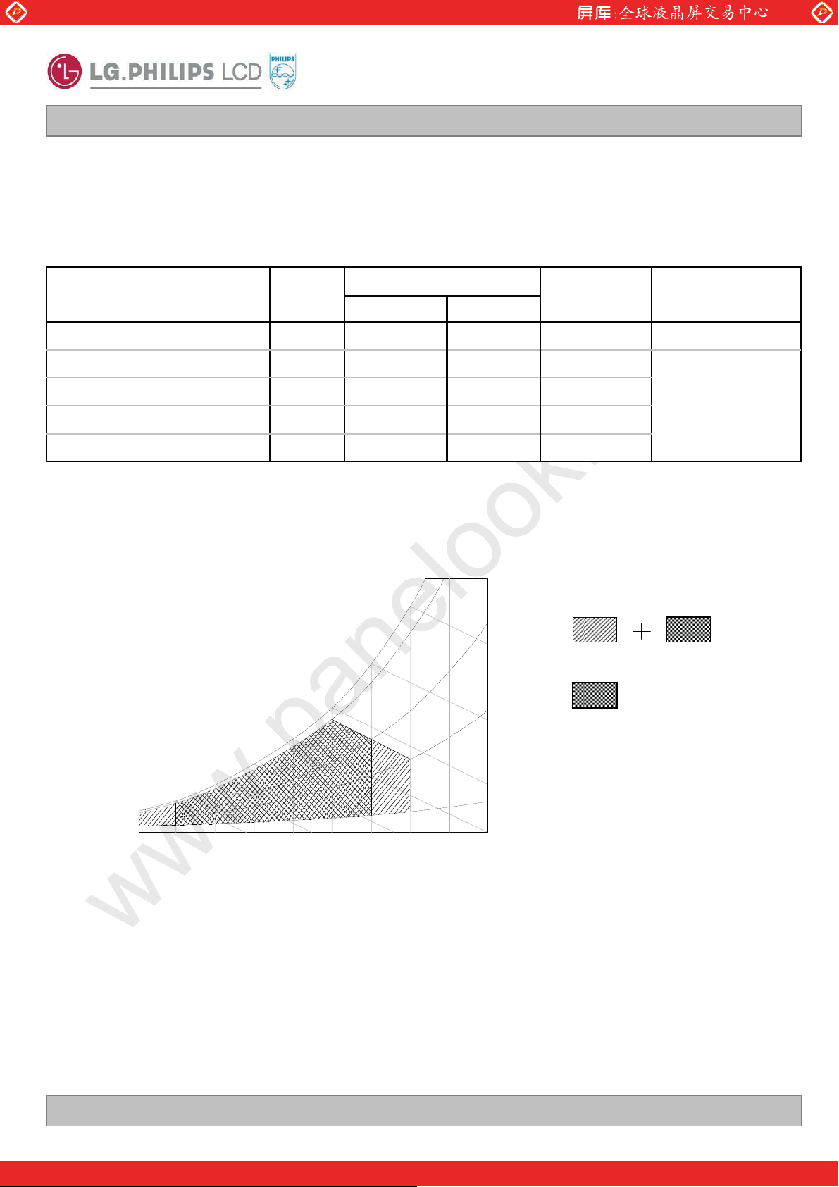
Note : 1. Temperature and relative humidity range are shown in the figure below.
Wet bulb temperature should be 39 ¶C Max, and no condensation of water.
ڔڋڀ
ڑڋ
ڑڋڀ
ڲۀۏٻڝېۇڽ
گۀۈۋۀۍڼۏېۍۀٻڶڞڸ
ڎڋ
ڍڋ
ڌڋ
ڋ
ڐڋ
ڏڋ
ڏڋڀ
ڣېۈۄڿۄۏ۔ٻڶڃڀڄڭڣڸ
ڌڋڀ
at 25 r 2¶C
1
ڮۏۊۍڼۂۀ
ڪۋۀۍڼۏۄۊۉ
ڌڋ ڍڋ ڎڋ ڏڋ ڐڋ ڑڋ ڒڋ ړڋڋڈڍڋ
ڟۍ۔ٻڝېۇڽٻگۀۈۋۀۍڼۏېۍۀٻڶڞڸ
Ver. 1.0 Jan. 01. 17. 2008
One step solution for LCD / PDP / OLED panel application: Datasheet, inventory and accessory!
5/ 35
www.panelook.com
Page 6
Global LCD Panel Exchange Center
www.panelook.com
LM240WU2
Liquid Crystal Display
Product Specification
3. Electrical Specifications
3-1. Electrical Characteristics
It requires two power inputs. One is employed to power the LCD electronics and to drive the TFT array and
liquid crystal. The second input power for the CCFL, is typically generated by an inverter. The inverter is an
external unit to the LCDs.
Table 2-1. ELECTRICAL CHARACTERISTICS
Parameter Symbol
MODULE :
ILCDPower Supply Input Current
Parameter Symbol
MODULE :
ILCDPower Supply Input Current
Values
Values
For SLB1/SLB3
MaxTypMin
Vdc12.612.011.4VLCDPower Supply Input Voltage
mVp-p400VdRFPermissive Power Input Ripple
NotesUnit
1mA570495-
2mA878675-
1Watt6.845.95-PLCDPower Consumption
3A3.0--IRUSHRush current
For SLB2
MaxTypMin
Vdc12.612.011.4VLCDPower Supply Input Voltage
mVp-p400VdRFPermissive Power Input Ripple
NotesUnit
1mA472410-
2mA667580-
1Watt5.664.92-PLCDPower Consumption
3A3.0--IRUSHRush current
Note :
1. The specified current and power consumption are under the V
whereas mosaic pattern(8 x 6) is displayed and f
is the frame frequency.
V
=12.0V, 25 r 2¶C,fV=60Hz condition
LCD
2. The current is specified at the maximum current pattern.
3. The duration of rush current is about 2ms and rising time of power Input is 1ms(min.).
White : 255Gray
Black : 0Gray
Mosaic Pattern(8 x 6)
Maximum current pattern
White Pattern
Ver. 1.0 Jan. 01. 17. 2008
One step solution for LCD / PDP / OLED panel application: Datasheet, inventory and accessory!
6/ 35
www.panelook.com
Page 7
Global LCD Panel Exchange Center
www.panelook.com
Product Specification
Table 2-2. INVERTER ELECTRICAL CHARACTERISTICS
LM240WU2
Liquid Crystal Display
Inverter :
Input Voltage
Input Current
Lamp Current
Open Lamp
Voltage
DDB
DDB
BInput Power
ON/OFFB/L on/off control
V
Vopen
ConditionSymbolParameter
No load
Vin=21.6V, Vbr=max
Values
Unit
Notes
Max.Typ.Min.
V26.424.021.6V
A3.022.75-Vin=24V, Vbr = maxI
Watt72.666-Vin=24V, Vbr = maxP
1
2
2
V5.0-2.0Lamp ON = High
V0.8-0.0Lamp OFF =Low
Vrms1150950750Vin=24V, Vbr=maxVoutLamp Voltage
mArms--2.5Vin=24V, Vbr=minIo(Min)
mArms4.74.23.7Vin=24V, Vbr=maxIo(Max)
V3.3-0Vin=24VVBRBrightness Adj
KHz484440Vbr=maxFoFrequency
Hz-180-Vin=24V, Vbr=minFbBurst Frequency
Vrms--1300
3%10.0--Vin=24VAsymmetry Ratio
31.55-1.27Vin=24VDistortion Ratio
Efficiency
TsStriking Time
Vin=21.6V, Vbr=max
Ɂ
No load
max
Sec2.0-1.0
%80Vin=24V Vbr=
LAMP :
4Hrs50,000Life time
Notes :
1. The input voltage ripple is limited below 400mVp-p.
2.The specified current and power consumption are under the typical supply Input voltage, 24V.
3. Voltage and current is measured for Asymmetry ratio and Distortion ratio.
Asymmetry Ratio: | Ipeak – I -peak | / IL Distortion Ratio : | Ipeak |(or I -peak |) / IL
4.The life is determined as the time at which luminance of the lamp is 50% compared to that of initial
value at the typical lamp current on condition of continuous operating at 25 r 2¶C.
5. Electrical characteristics are determined after the unit has been ‘ON’ and stable for approximately
30min in a dark environment at 25 ¶Cr 2¶C.
6. In case of the difference in measured values due to the difference of measuring device was found,
correlated value will be used after discussions between both parties.
Ver. 1.0 Jan. 01. 17. 2008
One step solution for LCD / PDP / OLED panel application: Datasheet, inventory and accessory!
7/ 35
www.panelook.com
Page 8
Global LCD Panel Exchange Center
www.panelook.com
LM240WU2
Liquid Crystal Display
Product Specification
3-2. Interface Connections
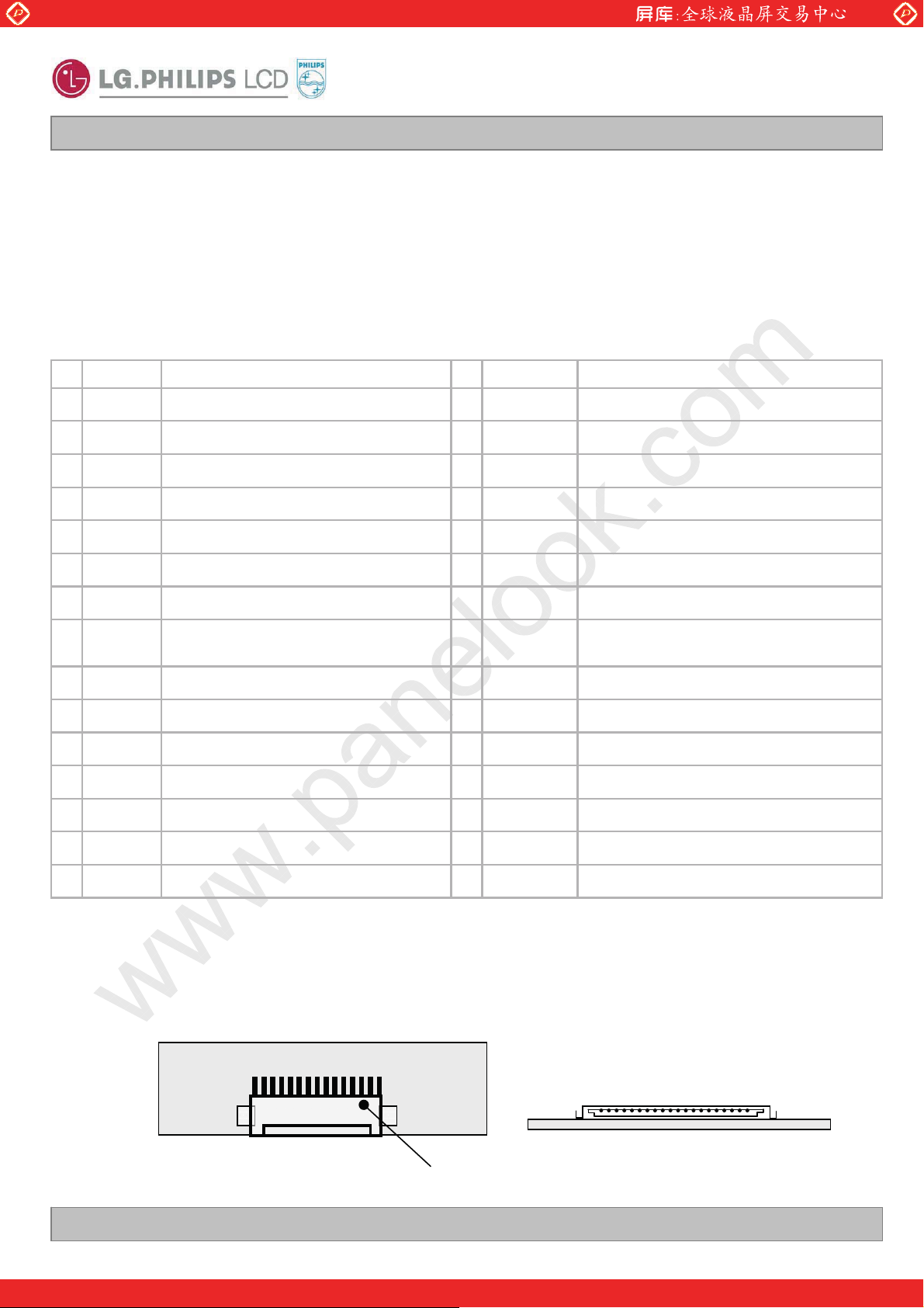
3-2-1. LCD Module
- LCD Connector(CN1). : GT103-30S-H23(LS Cable), ISL100-L30B-C23(UJU), KDF71G-30S-1H(HIROSE) or
equivalent
- Mating Connector: FI-X30C2L (Manufactured by JAE) or equivalent
Table 3 MODULE CONNECTOR(CN1) PIN CONFIGURATION
SymbolNo
FR0M1
FR0P2
FR1M3
FR1P4
FR2M5
FR2P6
GND7
FCLKINM8
FCLKINP9
FR3M10
FR3P11
SR0M12
SR0P13
Minus signal of odd channel 0 (LVDS)
Plus signal of odd channel 0 (LVDS)
Minus signal of odd channel 1 (LVDS)
Plus signal of odd channel 1 (LVDS)
Minus signal of odd channel 2 (LVDS)
Plus signal of odd channel 2 (LVDS)
Ground
Minus signal of odd clock channel
(LVDS)
Plus signal of odd clock channel (LVDS)
Minus signal of odd channel 3 (LVDS)
Plus signal of odd channel 3 (LVDS)
Minus signal of even channel 0 (LVDS)
Plus signal of even channel 0 (LVDS)
Description
No
16
SR1P
17
GND
18
SR2M
19
SR2P
20
SCLKINM
21
SCLKINP
22
SR3M
23
SR3P
24
GND
CLK_EDID
25
DATA_EDID
26
27
V_EDID
28
VLCD
Symbol
Description
Plus signal of even channel 1 (LVDS)
Ground
Minus signal of even channel 2 (LVDS)
Plus signal of even channel 2 (LVDS)
Minus signal of even clock channel (LVDS)
Plus signal of even clock channel (LVDS)
Minus signal of even channel 3 (LVDS)
Plus signal of even channel 3 (LVDS)
Ground
DDC for Clock
DDC for Data
DDC for Power 3.3V
Power Supply +12.0V
GND14
SR1M15
Ground
Minus signal of even channel 1 (LVDS)
29
30
VLCD
VLCD
Power Supply +12.0V
Power Supply +12.0V
Note: 1. All GND(ground) pins should be connected together and to Vss which should also be connected to
the LCD’s metal frame.
2. All V
LCD (power input) pins should be connected together.
3. Input Level of LVDS signal is based on the IEA 664 Standard.
User Connector Diagram
1
30
پڌ پڎڋ
Rear view of LCM
GT103-30S-H23(LS Cable)
Ver. 1.0 Jan. 01. 17. 2008
One step solution for LCD / PDP / OLED panel application: Datasheet, inventory and accessory!
www.panelook.com
8/ 35
Page 9
Global LCD Panel Exchange Center
www.panelook.com
Liquid Crystal Display
Product Specification
Table 4. REQUIRED SIGNAL ASSIGNMENT FOR Flat Link (TI:SN75LVDS83) Transmitter
Pin # Require SignalPin Name Pin # Require SignalPin Name
1 Power Supply for TTL InputVCC 29 Ground pin for TTLGND
2 TTL Input (R7)D5 30 TTL Input (DE)D26
3 TTL Input (R5)D6 31 TTL Level clock InputTXCLKIN
4 TTL Input (G0)D7 32 Power Down InputPWR DWN
5 Ground pin for TTLGND 33 Ground pin for PLLPLL GND
6 TTL Input (G1)D8 34 Power Supply for PLLPLL VCC
7 TTL Input (G2)D9 35 Ground pin for PLLPLL GND
LM240WU2
8 TTL Input (G6)D10 36 Ground pin for LVDSLVDS GND
9 Power Supply for TTL InputVCC 37 Positive LVDS differential data output 3TxOUT3ు
10 TTL Input (G7)D11 38 Negative LVDS differential data output 3TxOUT3ృ
11 TTL Input (G3)D12 39 Positive LVDS differential clock outputTXCLKOUTు
12 TTL Input (G4)D13 40 Negative LVDS differential clock outputTXCLKOUTృ
13 Ground pin for TTLGND 41 Positive LVDS differential data output 2TXOUT2ు
14 TTL Input (G5)D14 42 Negative LVDS differential data output 2TXOUT2ృ
15 TTL Input (B0)D15 43 Ground pin for LVDSLVDS GND
16 TTL Input (B6)D16 44 Power Supply for LVDSLVDS VCC
17 Power Supply for TTL InputVCC 45 Positive LVDS differential data output 1TXOUT1ు
46 Negative LVDS differential data output 1TXOUT1ృ18 TTL Input (B7)D17
19 TTL Input (B1)D18
20 TTL Input (B2)D19
22 TTL Input (B3)D20
47 Positive LVDS differential data output 0TXOUT0ు
48 Negative LVDS differential data output 0TXOUT0ృ
49 Ground pin for LVDSLVDS GND21 Ground pin for TTL InputGND
50 TTL Input (R6)D27
23 TTL Input (B4)D21
24 TTL Input (B5)D22
25 TTL Input (RSVD)D23
26 Power Supply for TTL InputVCC 54 TTL Input (R2)D2
51 TTL Input (R0)D0
52 TTL Input (R1)D1
53 Ground pin for TTLGND
55 TTL Input (R3)D327 TTL Input (HSYNC)D24
56 TTL Input (R4)D428 TTL Input (VSYNC)D25
Notes : Refer to LVDS Transmitter Data Sheet for detail descriptions.
Ver. 1.0 Jan. 01. 17. 2008
One step solution for LCD / PDP / OLED panel application: Datasheet, inventory and accessory!
9/ 35
www.panelook.com
Page 10
Global LCD Panel Exchange Center
www.panelook.com
Product Specification
3-2-2. Backlight Interface
-Inverter Connector : B14B-PH-SM3 Top entry type (Manufactured by JST) or Equivalent
- Mating Connector : PHR-14(Manufactured by JST) or Equivalent
Table 4. INVERTER CONNECTOR PIN CONFIGULATION
LM240WU2
Liquid Crystal Display
RemarksDescriptionSymbolPin No
BL1
BL2
BL3
BL4
BL5
ON12
BR13
Notes : 1. GND is connected to the LCD’s metal frame.
2. Vbr input is PWM signal and the signal level is within 3.3Vᇹ3%.
PWM Duty : Max 100% / Min 0%
Power Supply +24.0VV
Power Supply +24.0VV
Power Supply +24.0VV
Power Supply +24.0VV
Power Supply +24.0VV
Power GroundGND6
Power GroundGND7
Power GroundGND9
Power GroundGND10
NCOPEN11
Backlight On/off SignalV
NCStatus14
Note 1Power GroundGND8
(On :2.0V~5V/Off :0.0~0.8V)
Note 2Brightness Adjustable VoltageV
Rear view of LCM
PCB
14
…
…
1
B14B-PH-SM3
(JST : Japan Solderless Terminal Co.,Ltd.)
Ver. 1.0 Jan. 01. 17. 2008
One step solution for LCD / PDP / OLED panel application: Datasheet, inventory and accessory!
…
10 / 35
www.panelook.com
Page 11
Global LCD Panel Exchange Center
www.panelook.com
LM240WU2
Liquid Crystal Display
Product Specification
3-3. Signal Timing Specifications
This is signal timing required at the input of the TMDS transmitter. All of the interface signal timing should be
satisfied with the following specifications for it’s proper operation.
Table 5. TIMING TABLE (VESA COORDINATED VIDEO TIMING)
DCLK
Hsync
Vsync
SYMBOL
CLKPeriod
CLKFrequency
WHWidth-Active
VFrequency
WVWidth-Active
HVHorizontal Valid
HBPHorizontal Back Porch
HFPHorizontal Front Porch
NOTEUNITMAXTYPMINITEM
Ns6.336.416.49t
MHz158156152f
208820802072tHPPeriod
CLK
t
323232t
HP124712451243tVPPeriod
t
Hz60.5760.24159.91f
666t
192019201920t
888072t
504840t
tHP
t
CLK
Data
Enable
VVVertical Valid
VBPVertical Back Porch
VFPVertical Front Porch
120012001200t
373635t
432t
Note: Hsync period and Hsync width-active should be even number times of t
times of t
CLK, display control signal can be asynchronous. In order to operate this LCM a Hsync,
Vsyn, and DE(data enable) signals should be used.
1. The performance of the electro-optical characteristics may be influenced by variance of the vertical
refresh rates.
2. Vsync and Hsync should be keep the above specification.
3. Hsync Period, Hsync Width, and Horizontal Back Porch should be any times of of character
number(8).
4. The polarity of Hsync, Vsync is not restricted.
Ver. 1.0 Jan. 01. 17. 2008
WH+ tHBP+ tHFP168160152-Horizontal Blank
t
tHP
tWV+ tVBP+ tVFP474543-Vertical Blank
CLK. If the value is odd number
11 / 35
One step solution for LCD / PDP / OLED panel application: Datasheet, inventory and accessory!
www.panelook.com
Page 12

Global LCD Panel Exchange Center
3-4. Signal Timing Waveforms
www.panelook.com
LM240WU2
Liquid Crystal Display
Product Specification
Hsync, Vsync, DE, DATA
t
CLK
Dclk
INVALID
DATA
DE(Data Enable)
Hsync
t
WH
0.5VDD
0.7VDD
0.3VDD
VALID
Data are latched at the falling edge of DCLK
t
HP
INVALID
t
HBP
t
HV
t
HFP
DE(Data Enable)
t
VP
t
WV
Vsync
t
VBP
t
VV
t
VFP
DE(Data Enable)
Ver. 1.0 Jan. 01. 17. 2008
One step solution for LCD / PDP / OLED panel application: Datasheet, inventory and accessory!
12 / 35
www.panelook.com
Page 13

Global LCD Panel Exchange Center
www.panelook.com
LM240WU2
Liquid Crystal Display
Product Specification
3-5. Color Data Reference
The Brightness of each primary color(red,green,blue) is based on the 8-bit gray scale data input for the color;
the higher the binary input, the brighter the color. The table below provides a reference for color versus data
input.
Table 6. COLOR DATA REFERENCE
Input Color Data
Basic
Color
RED
Color
RED
MSB LSB
Black 0 0 0 0 0 0 0 00 0 0 0 0 0 0 00 0 0 0 0 0 0 0
Red (255)
Green (255)
Blue (255)
Cyan
Magenta
Yellow
White
GREEN
MSB LSB
BLUE
MSB LSB
B7 B6 B5 B4 B3 B2 B1 B0G7 G6 G5 G4 G3 G2 G1 G0R7 R6 R5 R4 R3 R2 R1 R0
0 0 0 0 0 0 0 00 0 0 0 0 0 0 01 1 1 1 1 1 1 1
0 0 0 0 0 0 0 01 1 1 1 1 1 1 10 0 0 0 0 0 0 0
1 1 1 1 1 1 1 10 0 0 0 0 0 0 00 0 0 0 0 0 0 0
1 1 1 1 1 1 1 11 1 1 1 1 1 1 10 0 0 0 0 0 0 0
1 1 1 1 1 1 1 10 0 0 0 0 0 0 01 1 1 1 1 1 1 1
0 0 0 0 0 0 0 01 1 1 1 1 1 1 11 1 1 1 1 1 1 1
1 1 1 1 1 1 1 11 1 1 1 1 1 1 11 1 1 1 1 1 1 1
0 0 0 0 0 0 0 00 0 0 0 0 0 0 00 0 0 0 0 0 0 0RED (000) Dark
0 0 0 0 0 0 0 00 0 0 0 0 0 0 00 0 0 0 0 0 0 1RED (001)
............
0 0 0 0 0 0 0 00 0 0 0 0 0 0 01 1 1 1 1 1 1 0RED (254)
0 0 0 0 0 0 0 00 0 0 0 0 0 0 01 1 1 1 1 1 1 1RED (255)
0 0 0 0 0 0 0 00 0 0 0 0 0 0 00 0 0 0 0 0 0 0GREEN (000) Dark
0 0 0 0 0 0 0 00 0 0 0 0 0 0 10 0 0 0 0 0 0 0GREEN (001)
GREEN
0 0 0 0 0 0 0 01 1 1 1 1 1 1 00 0 0 0 0 0 0 0GREEN (254)
0 0 0 0 0 0 0 01 1 1 1 1 1 1 10 0 0 0 0 0 0 0GREEN (255)
BLUE (000) Dark
0 0 0 0 0 0 0 00 0 0 0 0 0 0 00 0 0 0 0 0 0 0
0 0 0 0 0 0 0 10 0 0 0 0 0 0 00 0 0 0 0 0 0 0BLUE (001)
BLUE
1 1 1 1 1 1 1 00 0 0 0 0 0 0 00 0 0 0 0 0 0 0BLUE (254)
1 1 1 1 1 1 1 10 0 0 0 0 0 0 00 0 0 0 0 0 0 0BLUE (255)
Ver. 1.0 Jan. 01. 17. 2008
One step solution for LCD / PDP / OLED panel application: Datasheet, inventory and accessory!
............
............
13 / 35
www.panelook.com
Page 14

Global LCD Panel Exchange Center
3-6. Power Sequence
V
LCD
www.panelook.com
Product Specification
90%
LM240WU2
Liquid Crystal Display
90%
Power Supply, V
LCD
Interface Signal, V
(Digital RGB signal,
, H
SCDT ,V
sync
sync
, DE,
i
0V
0V
Clock to PanelLink
Transmitter)
Power Supply for Backlight
Inverter
Table 7. POWER SEQUENCE
10%
T1
T2 T5 T7
10%
T3
LAMP ONLAMP OFF
T4
T6
10%
10%
LAMP OFF
Values
Parameter
Notes : 1. Please avoid floating state of interface signal at invalid period.
2. When the interface signal is invalid, be sure to pull down the power supply for LCD V
3. Lamp power must be turn on after power supply for LCD and interface signal are valid.
Ver. 1.0 Jan. 01. 17. 2008
Units
MaxTypMin
ms10-1.0T1
ms50-0.01T2
ms--200T3
--200T4
ms
ms50-0.01T5
ms10-0.01T6
ms-400T7
to 0V.
LCD
14 / 35
One step solution for LCD / PDP / OLED panel application: Datasheet, inventory and accessory!
www.panelook.com
Page 15

Global LCD Panel Exchange Center
3-7. Power Sequence for Inverter
V
LCD
90%
www.panelook.com
LM240WU2
Liquid Crystal Display
Product Specification
Power Supply, V
Lamp ON/OFF
Lamp Dimmer
BL
0V
Vin_typ
10%
T1
T4
T2
LAMP ONLAMP OFF
T3
T5
Vin Dipping
0V
Table 8. POWER SEQUENCE
Parameter
Values
Vin_dip Vin_typ ϧ 0.2
MaxTypMin
--500T4
Units
ms30-1T1
ms--200T2
ms50--T3
ms
ms10--T5
Ver. 1.0 Jan. 01. 17. 2008
One step solution for LCD / PDP / OLED panel application: Datasheet, inventory and accessory!
15 / 35
www.panelook.com
Page 16

Global LCD Panel Exchange Center
www.panelook.com
LM240WU2
Liquid Crystal Display
Product Specification
4. Optical Specifications
Optical characteristics are determined after the unit has been ‘ON’ for approximately 30 minutes
in a dark environment at 25·2¶C. The values specified are at an approximate distance 50cm from the LCD
surface at a viewing angle of ) and T equal to 0 ¶ and aperture 1 degree.
FIG. 1 presents additional information concerning the measurement equipment and method.
Optical Stage(x,y)
LCD Module
FIG. 1 Optical Characteristic Measurement Equipment and Method
Table 9. OPTICAL CHARACTERISTICS
SymbolParameter
Surface Luminance, white
Luminance Variation
Response Time
Color Coordinates
[CIE1931]
Rise Time
Decay Time
RED
GREEN
BLUE
WHITE
G
WH
WHITE
Rx
Ry
Gx
Gy
Bx
By
Pritchard 880 or
equivalent
50cm
(Ta=25 ¶C, V
R
D
=12.0V, fV=60Hz Dclk=156MHz, VBR=3.3V)
LCD
Values
MaxTypMin
-800550CRContrast Ratio
-400320L
2
NotesUnits
1
2cd/m
3%30
4ms125.5-Tr
4ms126.5-Tr
0.640
0.340
0.290
Typ
-0.03
0.615
0.145
Typ
+0.03
0.070
0.313Wx
0.329Wy
Color Shift
Horizontal
Vertical
Viewing Angle (CR>10)
Horizontal
General
Vertical
Horizontal
Effective 7Degree
Vertical
T
CST_H
T
CST_V
T
GMA_H
T
GMA_V
T
H
T
V
-178-
-178-
-178170
-178170
-178
-178
Ver. 1.0 Jan. 01. 17. 2008
One step solution for LCD / PDP / OLED panel application: Datasheet, inventory and accessory!
5Degree
6Degree
82.2Gray Scale
16 / 35
www.panelook.com
Page 17

Global LCD Panel Exchange Center
www.panelook.com
Product Specification
Notes 1. Contrast Ratio(CR) is defined mathematically as :
LM240WU2
Liquid Crystal Display
RatioContrast
pixelswhiteallwithLuminanceSurface
pixels black all with Luminance Surface
It is measured at center point(Location P1)
2. Surface luminance(L
the surface with all pixels displaying white. For more information see FIG 2.
= = Average[ Lon1,Lon2,Lon3,Lon4,Lon5]
L
WH
3. The variation in surface luminance , G WHITE is defined as :
G
Where L1 to L13 are the luminance with all pixels displaying white at 13 locations.
4. Response time is the time required for the display to transition from black to white (Rise Time,
Tr
5. Color shift is the angle at which the color difference is lower than 0.04.
For more information see FIG 4.
WHITE
For more information see FIG 2.
) and from white to black (Decay Time, TrD). For additional information see FIG 3.
R
- Color difference (ȟu’v’)
WH)is luminance value at 5 points average across the LCD surface 50cm from
}}
)L .... ,L ,(L Average
on5on2on1
)L .. ,L,Minimum(L- )L .. ,L,Maximum(L
on13on2on1on13on2on1
(%)100
u
4
u
3122
yx
2
21
- Pattern size : 25% Box size
- Viewing angle direction of color shift : Horizontal, Vertical
6. Viewing angle is the angle at which the contrast ratio is greater than 10. The angles are
determined for the horizontal or x axis and the vertical or y axis with respect to the z axis which
is normal to the LCD surface. For more information see FIG 5.
7. Effective viewing angle is the angle at which the gamma shift of gray scale is lower than 0.3.
For more information see FIG 6 and FIG 7.
8. Gray scale specification
Gamma Value is approximately 2.2. For more information see Table 10.
'
v
21
'
x
9
y
3122
yx
u’1, v’1 : u’v’ value at viewing angle direction
2
)''()''('' vvuuvu '
u’2, v’2 : u’v’ value at front (ɂ=0)
Ver. 1.0 Jan. 01. 17. 2008
One step solution for LCD / PDP / OLED panel application: Datasheet, inventory and accessory!
17 / 35
www.panelook.com
Page 18

Global LCD Panel Exchange Center
www.panelook.com
Product Specification
Measuring point for surface luminance & measuring point for luminance variation.
H
A
LM240WU2
Liquid Crystal Display
H/16
67
B
V
V/10
A : H/4 mm
B : V/4 mm
@ H,V : Active Area
The response time is defined as the following figure and shall be measured by switching the input signal for
“black” and “white”.
9
11 12
FIG. 2 Measure Point for Luminance
2
1
4
3
5
Active Area
8
10
13
TrR
100
90
Optical
Response
10
0
Ver. 1.0 Jan. 01. 17. 2008
One step solution for LCD / PDP / OLED panel application: Datasheet, inventory and accessory!
black
FIG. 3 Response Time
white
TrD
black
18 / 35
www.panelook.com
Page 19

Global LCD Panel Exchange Center
www.panelook.com
Product Specification
Color shift is defined as the following test pattern and color.
LM240WU2
Liquid Crystal Display
25% Box size
FIG. 4 Test Pattern
Average RGB values in Bruce RGB for Macbeth Chart
Bluish greenBlue flowerFoliageBlue skyLight skinDark skin
114129778520698R
19911810211214256G
1781854616112345B
Orange yellowYellow greenPurpleModerate redPurplish blueOrange
2301607621156219R
162193396769104G
2958868717424B
cyanMagentaYellowRedGreenBlue
352072411977226R
126622122714832G
172151363765145B
blackNeutral 3.5Neutral 5Neutral 6.5Neutral 8White
2263110155206240R
2263110155206240G
2263110155206240B
Ver. 1.0 Jan. 01. 17. 2008
One step solution for LCD / PDP / OLED panel application: Datasheet, inventory and accessory!
19 / 35
www.panelook.com
Page 20

Global LCD Panel Exchange Center
Dimension of viewing angle range.
www.panelook.com
LM240WU2
Liquid Crystal Display
Product Specification
I
= 180q, Left
I
= 270q, Down
Normal
E
T
I
FIG. 5 Viewing angle
Y
I
= 90q, Up
I
= 0q, Right
FIG. 6 Sample Luminance vs. gray scale
(using a 256 bit gray scale)
r
LaVL
b
FIG. 7 Sample Log-log plot of luminance
vs. gray scale
b
Here the Parameter ¢ and ¤ relate the signal level V to the luminance L.
The GAMMA we calculate from the log-log representation (FIG. 7)
Ver. 1.0 Jan. 01. 17. 2008
One step solution for LCD / PDP / OLED panel application: Datasheet, inventory and accessory!
)log()log()log( aVrLL
20 / 35
www.panelook.com
Page 21

Global LCD Panel Exchange Center
Table 10. Gray Scale Specification
www.panelook.com
LM240WU2
Liquid Crystal Display
Product Specification
Relative Luminance [%] (Typ.)Gray Level
0.30
31
63
95
127
159
191
223
255
1.2
4.7
11.7
21.2
35.2
53.0
75.4
100
Ver. 1.0 Jan. 01. 17. 2008
One step solution for LCD / PDP / OLED panel application: Datasheet, inventory and accessory!
21 / 35
www.panelook.com
Page 22

Global LCD Panel Exchange Center
www.panelook.com
LM240WU2
Liquid Crystal Display
Product Specification
5. Mechanical Characteristics
The contents provide general mechanical characteristics. In addition the figures in the next page are detailed
mechanical drawing of the LCD.
546.4mmHorizontal
Outline Dimension
Bezel Area
Active Display Area
Surface Treatment
2,650g (Typ.) / 2,800g (Max.)Weight
Hard coating(2H)
Glare, Low Reflection treatment of the front polarizer
350.0mmVertical
28.9mmDepth
523.4mmHorizontal
329.0mmVertical
518.4mmHorizontal
324.0mmVertical
Notes : Please refer to a mechanic drawing in terms of tolerance at the next page.
Ver. 1.0 Jan. 01. 17. 2008
One step solution for LCD / PDP / OLED panel application: Datasheet, inventory and accessory!
22 / 35
www.panelook.com
Page 23

Global LCD Panel Exchange Center
<FRONT VIEW>
www.panelook.com
LM240WU2
Liquid Crystal Display
Product Specification
Ver. 1.0 Jan. 01. 17. 2008
One step solution for LCD / PDP / OLED panel application: Datasheet, inventory and accessory!
23 / 35
www.panelook.com
Page 24

Global LCD Panel Exchange Center
<REAR VIEW>
www.panelook.com
LM240WU2
Liquid Crystal Display
Product Specification
Ver. 1.0 Jan. 01. 17. 2008
One step solution for LCD / PDP / OLED panel application: Datasheet, inventory and accessory!
24 / 35
www.panelook.com
Page 25

Global LCD Panel Exchange Center
6. Reliability
Environment test condition
www.panelook.com
LM240WU2
Liquid Crystal Display
Product Specification
ConditionTest ItemNo
Ta= 60¶C 240hHigh temperature storage test1
Ta= -20¶C 240hLow temperature storage test2
Ta= 50¶C 50%RH 240hHigh temperature operation test3
Ta= 0¶C 240hLow temperature operation test4
Wave form : random
5
6
7
Vibration test
(non-operating)
Shock test
(non-operating)
Altitude
Operating
Storage / Shipment
Vibration level : 1.0G RMS
Bandwidth : 10-500Hz
Duration : X,Y,Z, 10 min
One time each direction
Shock level : 100Grms
Waveform : half sine wave, 2ms
Direction : ᇹX, ᇹY, ᇹZ
One time each direction
0 - 10,000 feet(3,048m)
0 - 40,000 feet(12,192m)
Ver. 1.0 Jan. 01. 17. 2008
One step solution for LCD / PDP / OLED panel application: Datasheet, inventory and accessory!
25 / 35
www.panelook.com
Page 26

Global LCD Panel Exchange Center
7. International Standards
7-1. Safety
a) UL 60950-1:2003, First Edition, Underwriters Laboratories, Inc.,
Standard for Safety of Information Technology Equipment.
b) CAN/CSA C22.2, No. 60950-1-03 1
Standard for Safety of Information Technology Equipment.
c) EN 60950-1:2001, First Edition,
European Committee for Electrotechnical Standardization(CENELEC)
European Standard for Safety of Information Technology Equipment.
www.panelook.com
Liquid Crystal Display
Product Specification
st
Ed. April 1, 2003, Canadian Standards Association,
LM240WU2
7-2. EMC
a) ANSI C63.4 “Methods of Measurement of Radio-Noise Emissions from Low-Voltage Electrical and
Electrical Equipment in the Range of 9kHZ to 40GHz. “American National Standards Institute(ANSI),
1992
b) C.I.S.P.R “Limits and Methods of Measurement of Radio Interface Characteristics of Information
Technology Equipment.“ International Special Committee on Radio Interference.
c) EN 55022 “Limits and Methods of Measurement of Radio Interface Characteristics of Information
Technology Equipment.“ European Committee for Electrotechnical Standardization.(CENELEC), 1998
( Including A1: 2000 )
Ver. 1.0 Jan. 01. 17. 2008
One step solution for LCD / PDP / OLED panel application: Datasheet, inventory and accessory!
26 / 35
www.panelook.com
Page 27

Global LCD Panel Exchange Center
8. Packing
8-1. Designation of Lot Mark
a) Lot Mark
ABCDEFGHI JKLM
A,B,C : SIZE(INCH) D : YEAR
E : MONTH F ~ M : SERIAL NO.
www.panelook.com
LM240WU2
Liquid Crystal Display
Product Specification
Note
1. YEAR
Year
Mark
2. MONTH
Month
Mark
b) Location of Lot Mark
Serial No. is printed on the label. The label is attached to the backside of the LCD module.
This is subject to change without prior notice.
8-2. Packing Form
a) Package quantity in one box : 6EA
b) Box Size : 436X346X613
2006720078200892009
6
Jun
6
Jul
7
Aug9Sep
8
321
200452005
4
Apr5May
4
200320022001
2010
0
Oct
A
Nov
B
DecMarFebJan
C321
Ver. 1.0 Jan. 01. 17. 2008
One step solution for LCD / PDP / OLED panel application: Datasheet, inventory and accessory!
27 / 35
www.panelook.com
Page 28

Global LCD Panel Exchange Center
www.panelook.com
LM240WU2
Liquid Crystal Display
Product Specification
9. PRECAUTIONS
Please pay attention to the followings when you use this TFT LCD module.
9-1. MOUNTING PRECAUTIONS
(1) You must mount a module using holes arranged in four corners or four sides.
(2) You should consider the mounting structure so that uneven force (ex. Twisted stress) is not applied to the
module. And the case on which a module is mounted should have sufficient strength so that external
force is not transmitted directly to the module.
(3) Please attach the surface transparent protective plate to the surface in order to protect the polarizer.
Transparent protective plate should have sufficient strength in order to the resist external force.
(4) You should adopt radiation structure to satisfy the temperature specification.
(5) Acetic acid type and chlorine type materials for the cover case are not desirable because the former
generates corrosive gas of attacking the polarizer at high temperature and the latter causes circuit break
by electro-chemical reaction.
(6) Do not touch, push or rub the exposed polarizers with glass, tweezers or anything harder than HB
pencil lead. And please do not rub with dust clothes with chemical treatment.
Do not touch the surface of polarizer for bare hand or greasy cloth.(Some cosmetics are detrimental
to the polarizer.)
(7) When the surface becomes dusty, please wipe gently with absorbent cotton or other soft materials like
chamois soaks with petroleum benzene. Normal-hexane is recommended for cleaning the adhesives
used to attach front / rear polarizers. Do not use acetone, toluene and alcohol because they cause
chemical damage to the polarizer.
(8) Wipe off saliva or water drops as soon as possible. Their long time contact with polarizer causes
deformations and color fading.
(9) Do not open the case because inside circuits do not have sufficient strength.
9-2. OPERATING PRECAUTIONS
(1) The spike noise causes the mis-operation of circuits. It should be lower than following voltage :
V=·200mV(Over and under shoot voltage)
(2) Response time depends on the temperature.(In lower temperature, it becomes longer.)
(3) Brightness depends on the temperature. (In lower temperature, it becomes lower.)
And in lower temperature, response time(required time that brightness is stable after turned on) becomes
longer.
(4) Be careful for condensation at sudden temperature change. Condensation makes damage to polarizer or
electrical contacted parts. And after fading condensation, smear or spot will occur.
(5) When fixed patterns are displayed for a long time, remnant image is likely to occur.
(6) Module has high frequency circuits. Sufficient suppression to the electromagnetic interference shall be
done by system manufacturers. Grounding and shielding methods may be important to minimized the
interference.
(7) Please do not give any mechanical and/or acoustical impact to LCM. Otherwise, LCM can’t be operated
its full characteristics perfectly.
(8) A screw which is fastened up the steels should be a machine screw.
(if not, it causes metallic foreign material and deal LCM a fatal blow)
(9) Please do not set LCD on its edge.
Ver. 1.0 Jan. 01. 17. 2008
28 / 35
One step solution for LCD / PDP / OLED panel application: Datasheet, inventory and accessory!
www.panelook.com
Page 29

Global LCD Panel Exchange Center
www.panelook.com
LM240WU2
Liquid Crystal Display
Product Specification
9-3. ELECTROSTATIC DISCHARGE CONTROL
Since a module is composed of electronic circuits, it is not strong to electrostatic discharge. Make certain that
treatment persons are connected to ground through wrist band etc. And don’t touch interface pin directly.
9-4. PRECAUTIONS FOR STRONG LIGHT EXPOSURE
Strong light exposure causes degradation of polarizer and color filter.
9-5. STORAGE
When storing modules as spares for a long time, the following precautions are necessary.
(1) Store them in a dark place. Do not expose the module to sunlight or fluorescent light. Keep the temperature
between 5¶C and 35¶C at normal humidity.
(2) The polarizer surface should not come in contact with any other object.
It is recommended that they be stored in the container in which they were shipped.
9-6. HANDLING PRECAUTIONS FOR PROTECTION FILM
(1) The protection film is attached to the bezel with a small masking tape.
When the protection film is peeled off, static electricity is generated between the film and polarizer.
This should be peeled off slowly and carefully by people who are electrically grounded and with well ionblown equipment or in such a condition, etc.
(2) When the module with protection film attached is stored for a long time, sometimes there remains a very
small amount of glue still on the bezel after the protection film is peeled off.
(3) You can remove the glue easily. When the glue remains on the bezel surface or its vestige is recognized,
please wipe them off with absorbent cotton waste or other soft material like chamois soaked with normalhexane.
Ver. 1.0 Jan. 01. 17. 2008
One step solution for LCD / PDP / OLED panel application: Datasheet, inventory and accessory!
29 / 35
www.panelook.com
Page 30

Global LCD Panel Exchange Center
www.panelook.com
Product Specification
10. EDID DATA FOR LM240WU2-SLB1 & LM240WU2-SLB3
LM240WU2
Liquid Crystal Display
Byte#
8
18
Field Name and Comments
EISA Manuf. Code LSB ( 3 character ID =
APP
ucture Ver # = 112
Feature support (DPMS) = Active off, RGB
color
Green X Gx =0.2901D
Green Y Gy =0.6151E
4A
9D
ValueValue
(binary)(HEX)(HEX)
0000000000Header0
11111111FF1
11111111FF2
Header11111111FF3
11111111FF4
11111111FF5
11111111FF6
00000000007
0000011006
0001000010Compressed ASCII9
100011018DProduct Code (9C,8D)0A
100111009CHex, LSB first0B
00000001010E
00000001010F
0000000000Week of manufacture10
0001000111Year of manufacture 200711
1000000080Video input definition 14
0111100078Display Gamma = 2.217
000010100A
11000111C7Red/Green low Bits19
0111010074Blue/White Low Bits1A
10101000A3Red X Rx =0.6401B
0101001057Red Y Ry =0.3401C
0010010125Blue X Bx =0.1451F
0001000111Blue Y By =0.07020
0101000050White X Wx = 0.31321
0101010054White Y Wy = 0.32922
0001000010Manufacturer's timings25
0000000101Standard timing #1 was not used26
000000010127
0000000101Standard timing #2 was not used28
000000010129
product ID for LM240WU2-SLB1 &
LM240WU2-SLB3 = 9C8D
Vender/000000010132-bit serial #0C
Product ID00000001010D
EDID Version/0000000101EDID Str
Revision0000001103EDID revision # = 313
Display 0011010034Max H image size = 52cm15
Parameter0010000020Max V image size =32cm16
Color00110100
Characteristic10101001
Established0000000000Established timing 123
Timings0000000000Established timing 2 24
kAppleNoncoherentTMDSFlag
= 0x10, kAppleCoherentTMDSFla
g = 0x08
Ver. 1.0 Jan. 01. 17. 2008
One step solution for LCD / PDP / OLED panel application: Datasheet, inventory and accessory!
30 / 35
www.panelook.com
Page 31

Global LCD Panel Exchange Center
www.panelook.com
LM240WU2
Liquid Crystal Display
Product Specification
Byte#
47
4C
4D
4E
4F
50
51
Field Name and Comments
H sync. Width= 32 pixels3F
Non-interlaced, Normal display, No stereo,
Digital separate sync, H/V pol Negatives
Version
Apple edid signature
Apple edid signature
Link Type (LVDS, Dual Link, MSB)
Pixel and link component format (8bit)
Panel features
ValueValue
(binary)(HEX)(HEX)
0000000101Standard timing #3 was not used2A
00000001012B
Standard0000000101Standard timing #4 was not used2C
Timing ID00000001012D
0000000101Standard timing #5 was not used2E
00000001012F
0000000101Standard timing #6 was not used30
000000010131
0000000101Standard timing #7 was not used32
000000010133
0000000101Standard timing #8 was not used34
000000010135
11110000F0Detailed timing/monitor36
001111003CPixel Clock = 156 MHz37
1000000080Hor active= 1920 pixels38
10100000A0Hor blanking= 160 pixels39
01110000703A
10110000B0Vertcal active= 1200 lines3B
Detailed001011012DVertical blanking= 45 lines3C
Timing01000000403D
1000030H sync. Offset= 48 pixels3E
0011011036V sync. Offset= 3 lines40
0000000000V sync. Width= 6 lines41
0000011006H image size= 518 mm42
0100010044V image size = 324 mm43
000100011144
0000000000No Horizontal Border45
0000000000No Vertical Border46
000111101E
0000000000Detailed timing/monitor48
0000000000descriptor #249
00000000004A
00000001014B
0000000000
0000011006
000000000052
000000000053
000000000054
000000000055
000000000056
000000000057
000010100A58
001000002059
Description001
#10010000020
Detailed0001000010
Timing0011000030
Description0001000111
#20000000101
Ver. 1.0 Jan. 01. 17. 2008
One step solution for LCD / PDP / OLED panel application: Datasheet, inventory and accessory!
31 / 35
www.panelook.com
Page 32

Global LCD Panel Exchange Center
www.panelook.com
LM240WU2
Liquid Crystal Display
Product Specification
Byte#
64
65
68
6A
6B
Field Name and Comments
“
w"
“
U"
“
S"
“
B"
“
1"
Checksum7F
45
ValueValue
(binary)(HEX)(HEX)
0000000000Detailed timing/monitor5A
0000000000descriptor #35B
0000000000LM240WU2-SLB15C
11111110FE5D
00000000005E
010011004C"L"5F
Detailed010011014D"M"60
Timing0011001032"2"61
Description0011010034"4"62
#30011000030"0"63
0101011157
Asc
ii Data String:0101010155
0011001032"2"66
001011012D"-"67
0101001153
010011004C"L"69
0100001042
0011000131
0000000000Detailed timing/monitor6C
0000000000descriptor #46D
0000000000Color LCD6E
11111100FC6F
000000000070
0100001143C71
001000002076
0100010044D79
000010100A7A
00100000207B
00100000207C
00100000207D
LM240WU2-SLB1
Detailed011011116Fo72
Timing011011006Cl73
Description011011116Fo74
#40111001072r75
Monitor Name:010011004CL77
Color LCD0100001143C78
Extension Flag0000000000Extension Flag = 007E
Checksum01000101
Ver. 1.0 Jan. 01. 17. 2008
One step solution for LCD / PDP / OLED panel application: Datasheet, inventory and accessory!
32 / 35
www.panelook.com
Page 33

Global LCD Panel Exchange Center
www.panelook.com
Product Specification
10. EDID DATA FOR LM240WU2-SLB2
LM240WU2
Liquid Crystal Display
Byte#
8
18
Field Name and Comments
EISA Manuf. Code LSB ( 3 character ID =
APP
ucture Ver # = 112
Feature support (DPMS) = Active off, RGB
color
Green X Gx =0.2901D
Green Y Gy =0.6151E
4A
9D
ValueValue
(binary)(HEX)(HEX)
0000000000Header0
11111111FF1
11111111FF2
Header11111111FF3
11111111FF4
11111111FF5
11111111FF6
00000000007
0000011006
0001000010Compressed ASCII9
100011108EProduct Code (9C,8E)0A
100111009CHex, LSB first0B
00000001010E
00000001010F
0000000000Week of manufacture10
0001000111Year of manufacture 200711
1000000080Video input definition 14
0111100078Display Gamma = 2.217
000010100A
11000111C7Red/Green low Bits19
0111010074Blue/White Low Bits1A
10101000A3Red X Rx =0.6401B
0101001057Red Y Ry =0.3401C
0010010125Blue X Bx =0.1451F
0001000111Blue Y By =0.07020
0101000050White X Wx = 0.31321
0101010054White Y Wy = 0.32922
0001000010Manufacturer's timings25
0000000101Standard timing #1 was not used26
000000010127
0000000101Standard timing #2 was not used28
000000010129
product ID for LM240WU2-SLB2
= 9C8E
Vender/000000010132-bit serial #0C
Product ID00000001010D
EDID Version/0000000101EDID Str
Revision0000001103EDID revision # = 313
Display 0011010034Max H image size = 52cm15
Parameter0010000020Max V image size =32cm16
Color00110100
Characteristic10101001
Established0000000000Established timing 123
Timings0000000000Established timing 2 24
kAppleNoncoherentTMDSFlag
= 0x10, kAppleCoherentTMDSFla
g = 0x08
Ver. 1.0 Jan. 01. 17. 2008
One step solution for LCD / PDP / OLED panel application: Datasheet, inventory and accessory!
33 / 35
www.panelook.com
Page 34

Global LCD Panel Exchange Center
www.panelook.com
LM240WU2
Liquid Crystal Display
Product Specification
Byte#
47
4C
4D
4E
4F
50
51
Field Name and Comments
H sync. Width= 32 pixels3F
Non-interlaced, Normal display, No stereo,
Digital separate sync, H/V pol Negatives
Version
Apple edid signature
Apple edid signature
Link Type (LVDS, Dual Link, MSB)
Pixel and link component format (8bit)
Panel features
ValueValue
(binary)(HEX)(HEX)
0000000101Standard timing #3 was not used2A
00000001012B
Standard0000000101Standard timing #4 was not used2C
Timing ID00000001012D
0000000101Standard timing #5 was not used2E
00000001012F
0000000101Standard timing #6 was not used30
000000010131
0000000101Standard timing #7 was not used32
000000010133
0000000101Standard timing #8 was not used34
000000010135
11110000F0Detailed timing/monitor36
001111003CPixel Clock = 156 MHz37
1000000080Hor active= 1920 pixels38
10100000A0Hor blanking= 160 pixels39
01110000703A
10110000B0Vertcal active= 1200 lines3B
Detailed001011012DVertical blanking= 45 lines3C
Timing01000000403D
1000030H sync. Offset= 48 pixels3E
0011011036V sync. Offset= 3 lines40
0000000000V sync. Width= 6 lines41
0000011006H image size= 518 mm42
0100010044V image size = 324 mm43
000100011144
0000000000No Horizontal Border45
0000000000No Vertical Border46
000111101E
0000000000Detailed timing/monitor48
0000000000descriptor #249
00000000004A
00000001014B
0000000000
0000011006
000000000052
000000000053
000000000054
000000000055
000000000056
000000000057
000010100A58
001000002059
Description001
#10010000020
Detailed0001000010
Timing0011000030
Description0001000111
#20000000101
Ver. 1.0 Jan. 01. 17. 2008
One step solution for LCD / PDP / OLED panel application: Datasheet, inventory and accessory!
34 / 35
www.panelook.com
Page 35

Global LCD Panel Exchange Center
www.panelook.com
LM240WU2
Liquid Crystal Display
Product Specification
Byte#
64
65
68
6A
6B
Field Name and Comments
“
w"
“
U"
“
S"
“
B"
“
2"
Checksum7F
43
ValueValue
(binary)(HEX)(HEX)
0000000000Detailed timing/monitor5A
0000000000descriptor #35B
0000000000LM240WU2-SLB25C
11111110FE5D
00000000005E
010011004C"L"5F
Detailed010011014D"M"60
Timing0011001032"2"61
Description0011010034"4"62
#30011000030"0"63
0101011157
Asc
Data String:0101010155
ii
0011001032"2"66
001011012D"-"67
0101001153
010011004C"L"69
0100001042
0011001032
0000000000Detailed timing/monitor6C
0000000000descriptor #46D
0000000000Color LCD6E
11111100FC6F
000000000070
0100001143C71
001000002076
0100010044D79
000010100A7A
00100000207B
00100000207C
00100000207D
LM240WU2-SLB2
Detailed011011116Fo72
Timing011011006Cl73
Description011011116Fo74
#40111001072r75
Monitor Name:010011004CL77
Color LCD0100001143C78
Extension Flag0000000000Extension Flag = 007E
Checksum01000011
Ver. 1.0 Jan. 01. 17. 2008
One step solution for LCD / PDP / OLED panel application: Datasheet, inventory and accessory!
35 / 35
www.panelook.com
 Loading...