

Page 1

LM157E2-A2
Product Specification
SPECIFICATION
FOR
APPROVAL
(
) Preliminary Specification
(
) Final Specification
Title 15.7” SXGA TFT LCD
BUYER DID(Gateway) SUPPLIER LG.Philips LCD Co., Ltd.
MODEL *MODEL LM157E2
SUFFIX A2
* When you obtain standard
please use the above model name without suffix.
SIGNATURE
/
/
/
DATE APPROVED BY
* When you obtain standard approval ,
* When you obtain standard * When you obtain standard
please use the above model name without suffix.
please use the above model name without suffix.please use the above model name without suffix.
S.H. Kang / G.Manager
REVIEWED BY
B.K. Kim / Manager
J.T. Kim / Manager
PREPARED BY
S.H.Kim / Engineer
K.K.Jang / Manager
approval ,
approval ,approval ,
DATE
Please return 1 copy for your confirmation
with your signature and comments.
The preliminary document is subject to change without prior notice.
Ver 1.0 SEP 30, 2000 Page 1/24
Product Engineering Dept.
LG.Philips LCD Co., Ltd.
Page 2

LM157E2-
A2
Product Specification
CONTENTS
NO. ITEM Page
- COVER 1
-CONTENTS 2
- RECORD OF REVISION 3
1 GENERAL DESCRIPTION 4
2 MAXIMUM RATINGS 5
3 ELECTRICAL SPECIFICATIONS 6
3-1 ELECTRICAL CHARACTERISTICS 6
3-2 INTERFACE CONNECTION 7
3-3 SIGNAL TIMING SPECIFICATIONS 9
3-4 SIGNAL TIMING WAVE FORMS 10
3-5 COLOR INPUT DATA REFERENCE 11
3-6 POWER SEQUENCE 12
4 OPTICAL SPECIFICATIONS 13
5 MECHANICAL CHARACTERISTICS 15
6RELIABILITY 18
7 INTERNATIONAL STANDARDS 19
7-1 SAFETY 19
7-2 EMC 19
8 PACKING 20
8-1 DESIGNATION OF LOT MARK 20
8-2 PACKING FORM 20
9 PRECAUTIONS 21
APPENDIX 23
A-1 OPTICAL CHARACTERISTIC MEASUREMENT EQUIPMENT AND METHOD 23
A-2 LUMINANCE 23
A-3 RESPONSE TIME 23
A-4 VIEWING ANGLE 24
Ver 1.0 SEP 30, 2000 Page 2/24
Page 3

LM157E2-
Product Specification
RECORDS OF REVISIONS
Version No Date Page DESCRIPTION
A2
1.0 SEP.30, 2000 -
Final Specification
Ver 1.0 SEP 30, 2000 Page 3/24
Page 4

LM157E2-
A2
Product Specification
1. General Description
The LM157E2-A2 is a Color Active Matrix Liquid Crystal Display with an integral Cold Cathode
Fluorescent Lamp(CCFL) back light system. The m atrix employs a-Si Thin F ilm Transistor as the active
element. It is a transmiss ive type display operating in the normally white mode. This TFT -LCD has a 15.7
inch diagonally measured active display area with SXGA resolution(1024 vertic al by 1280 horizontal pixel
array). Each pix el is divided into Red, Green and Blue sub-pixels or dots which are arranged in vertical
stripes. Gray scale or the brightness of the sub- pixel color is determined with a 8-bit gray scale s ignal
for each dot, thus, presenting a palette of more than 16,777,216 colors.
The LM157E2-A2 has been designed to apply the interface method that enables low power, high speed
low EMI. FPD Link must be used as a LVDS(Low Voltage Differential Signaling) chip.
The LM157E2-A2 is intended to support applic ations where thin thickness and low power consumption
are critical factors and graphic displays are im portant. In com bination with the vertic al arrangem ent of the
sub-pixels, the LM157E2-A2 characteristic s provide an excellent flat panel display for office automation
products such as monitors.
RGB
Column Driver
LVDS
Pair#1
Timing Control
LVDS
Pair #2
CN2
& LVDS 1Chip
Power
Block
G1
Row
Driver
circuiit
G1024
S1
TFT-LCD
(1280 x RGB x 1024
Backlight 2EA
S1280
General Features
The following are general feature of the model LM157E1-A2 LCD;
Active screen size 15.7 inches(39.832cm) diagonal
Outline dimensions 335.0(H) 273.5(V) 11.2(D) mm (Typ.)
Pixel pitch 0.243 mm 0.243 mm
Pixel format 1280 horiz. By 1024 vert. pixels
RGB stripe arrangement
Color depth 8-bit, 16,777,216 colors
Luminance,White 200 cd/m
Power Consumption Total 12.57 Watt,typ (2.97 Watt @IV
Weight 1140g (typ)
Display operating mode Transmissive mode, normally white
Surface treatments Hard coating(3H),
A
nti-glare treatment of the front polarizer
2
(5point Average.)
, 9.6Watt@200cd/m2 [Lamp])
AA
Ver 1.0 SEP 30, 2000 Page 4/24
Page 5

LM157E2-
A2
Product Specification
2. Maximum Ratings
The following are maximum values which, if exceeded, may cause faulty operation or damage to the unit.
Table 1. ABSOLUTE MAXIMUM RATINGS
Parameter Symbol
Values
Min. Max.
Units Notes
Power Input Voltage
Operating Temperature
Storage Temperature
V
cc
T
OP
T
ST
-0.3
0
-20
+3.5
+50
+60
Vdc
Note: 1. Temperature at 5mm above display center of LCD Module.
Ta 40 : 90%RH Max
Ta 40 : Absolute Humidity shall be less than Ta = 40 90%RH .
These shall be no dew condensation.
2. Humidity Min. 5%RH, Max. 95%RH
3. Temperature and relative humidity range are shown in the figure below.
Wet bulb temperature should be 39 max, and no condention of water.
95% 80%
%
60
40
%
Storage
Wet Bulb
Temperature []
60
50
40
at 25
1,2
1,2
-20
30
20
0
0
0
20 30 40
50
60 70 800
20
5
%
%
Operation
Humidity [(%)RH]
Dry Bulb Temperature []
Ver 1.0 SEP 30, 2000 Page 5/24
Page 6

LM157E2-
A2
Product Specification
3. Electrical Specifications
3-1. Electrical Characteristics
The LM157E2-A2 requires two power inputs. One is employed to power the LCD electronics and to
drive the TFT array and liquid crystal. The other input which powers the CCFL, is typically generated by
an inverter. The inverter is an external unit to the LCD.
Table 2. ELECTRICAL CHARACTERISTICS
Parameter Symbol
MODULE:
Power Supply Input Voltage
Power Supply Input Current
Differential Impedance
Power Consumption
Vcc
Icc
Zm
Pc
Min. Typ. Max.
3.1
-
90
-
LAMP
Operating Voltage
Operating Current
Established Starting Voltage
at 25
at 0
Operating Frequency
Discharge Stabilization Time
Power Consumption(2CCFL’s)
Life Time
V
BL
I
BL
f
BL
T
S
P
BL
590
(3.0)
30,000
(8.5mA)
-
-
40
-
-
Note)The design of the inverter must have specifications for the lamp in LCD Assembly.
The performance of the Lamp in LCM, for example life time or brightness, is extremely influenced by the
characteristics of the DC-AC Inverter. So all the parameters of an inverter should be carefully designed
so as not to produce too much leakage current from high-voltage output of the inverter.
When you design or order the inverter, please make sure unwanted lighting caused by the mismatch of
the lamp and the inverter(no lighting, flicker, etc) never occurs. When you confirm it, the LCD Assembly
should be operated in the same condition as installed in your instrument
Notes:1. The current draw and power consumption specified is for 3.3 Vdc at 25and fv at 60Hz.
(at chess 8X6 pattern)
2. The variance of the voltage is 10%.
3. The output voltage at the transformer in the inverter must be high considering to the loss of the
ballast capacitor in the inverter.
4. The output of the inverter must have symmetrical(negative and positive) voltage waveform and
symmetrical current waveform.(Unsymmetrical ratio is less than 10%) Please do not use the
inverter which has unsymmetrical voltage and unsymmetrical current and spike wave.
Lamp frequency may produce interference with horizontal synchronous frequency and as a result
this may cause beat on the display. Therefore lamp frequency shall be as away as possible from
the horizontal synchronous frequency and from its harmonics in order to prevent interference.
5. The lamp power consumption shown above does not include loss of external inverter.
6. Let’s define the brightness of the lamp after being lighted for 5 minutes as 100%.
T
is the time required for the brightness of the center of the lamp to be not less than 95%.
s
7. The life time is determined as the time at which brightness of lamp is 50% compare to that of
initial value at the typical lamp current on condition of continuous operating at 25 2.
Values
3.3
900
100
2.97
600
(8.0)
58
9.6
(8mA)
-
-
3.5
1400
110
4.62
730
(8.5)
(865)
(1210)
80
10.6
(3mA)
3
-
.
Units Notes
Vdc
mA
Ohm
Watt
V
RMS
mA
V
RMS
V
RMS
KHz
Minutes
Watts
Hrs
1
1
2
3
4
6
5
7
Ver 1.0 SEP 30, 2000 Page 6/24
Page 7

LM157E2-
A2
Product Specification
3-2. Interface Connections
Interface chip must be used LVDS, part No. DS90CF383MTD(Transmitter), DS90CF384MTD(Receiver)
made by National Semiconductor. Or used the compatible interface chips(TI : SN75LVDS83, Thine).
This LCD employs three inter face connections. A 30-pin connector is used for the module electronics
interface and power interface.
The electronics interface connector is a model DF19K-30P-H manufactured by HIROSE. The pin
configuration for the connector is shown in the table 3.
Table 3. MODULE CONNECTOR PIN CONFIGURATION (LVDS)
Pin Symbol Description Notes
1
2
3
4
5
6
7
8
9
10
11
12
13
14
15
16
17
18
19
20
21
22
23
24
25
26
27
28
29
30
3.3V
3.3V
3.3V
3.3V
GND
GND
E_RX0-
E_RX0+
E_Rx1-
E_RX1+
E_RX2-
E_RX2+
E_RXC-
E_RXC+
E_RX3-
E_RX3+
GND
GND
O_RX0-
O_RX0+
O_RX1-
O_RX1+
O_RX2O_RX2+
O_RXC-
O_RXC+
O_RX3O_RX3+
GND
GND
3.3V
3.3V
3.3V
3.3V
GROUND
GROUND
Minus Signal of Even Channel 0 (LVDS)
Plus Signal of Even Channel 0 (LVDS)
Minus Signal of Even Channel 1 (LVDS)
Plus Signal of Even Channel 1 (LVDS)
Minus Signal of Even Channel 2 (LVDS)
Plus Signal of Even Channel 2 (LVDS)
Minus Signal of Even Clock Channel(LVDS)
Plus Signal of Even Clock Channel(LVDS)
Minus Signal of Even Channel 3 (LVDS)
Plus Signal of Even Channel 3 (LVDS)
GROUND
GROUND
Minus Signal of Odd Channel 0 (LVDS)
Plus Signal of Odd Channel 0 (LVDS)
Minus Signal of Odd Channel 1 (LVDS)
Plus Signal of Odd Channel 1 (LVDS)
Minus Signal of Odd Channel 2 (LVDS)
Plus Signal of Odd Channel 2 (LVDS)
Minus Signal of Odd Clock Channel(LVDS)
Plus Signal of Odd Clock Channel(LVDS)
Minus Signal of Odd Channel3(LVDS)
Plus Signal of Odd Channel3(LVDS)
GROUND
GROUND
Second Data
First Data
30
Transparent View
Ver 1.0 SEP 30, 2000 Page 7/24
Page 8

LM157E2-
A2
Product Specification
The backlight interface connector is a model BHR-03VS-1, manufactored by JST. The mating connector
part number is SM02(8.0)B-BHS-1-TB or equivalent. The pin configuration for the connector is shown in
The table below.
Table 4. BACKLIGHT CONNECTOR PIN CONFIGURATION
Pin Symbol Description Notes
1
2
3
HV
Open
LV
Lamp power input
Open
GROUND
1
2
Notes: 1. The input power terminal is colored pink . Ground pin color is white.
2. The lamp ground should be common with GND.
Table 5 Required Signal A ssignment for FlatLink
Pin # Pin Name Required Signals Pin # Pin Name Required Signals
1 Vcc Power supply for TTL input 29 GND Ground pin for TTL
2 D5 TTL Input(R7) 30 D26 TTL Input (Data Enable)
3 D6 TTL Input (R5) 31 TxCLKIN TTL Input clock input
4 D7 TTL Input (G0) 32 PWR DWN Power down input
5 GND Ground pin f or TTL 33 PLL GND Ground pin for PLL
6 D8 TTL Input (G1) 34 PLL VCC Power supply f or P LL
7 D9 TTL Input (G2) 35 PLL GND Ground pin for PLL
8 D10 TTL Input (G6) 36 LVDS GND Ground pin for LVDS
9 Vcc Power supply for TTL input 37 TxOUT3+ Positive LVDS differential dat a output 3
10 D11 TTL Input (G7) 38 TxOUT3- Negative LVDS differential data output 3
11 D12 TTL Input (G3) 39 TxCLKOUT+ Positive LVDS differential clock output
12 D13 TTL Input (G4) 40 TxCLKOUT- Negative LVDS differential cl ock output
13 GND Ground pin for TTL 41 TxOUT2+ Positive LVDS diff erential data output 2
14 D14 TTL Input (G5) 42 TxOUT2- Negative LVDS differential data output 2
15 D15 TTL Input (B0) 43 LVDS GND Ground pin for LVDS
16 D16 TTL Input (B6) 44 LVDS Vcc Power supply for LVDS
17 Vcc Power supply for TTL input 45 TxOUT1+ Positive LVDS differential data output 1
18 D17 TTL Input (B7) 46 TxOUT1- Negative LVDS differential data output 1
19 D18 TTL Input (B1) 47 TxOUT0+ Positive LVDS differential data output 0
20 D19 TTL Input (B2) 48 TxOUT0- Negative LVDS differential data output 0
21 GND Ground pin for TTL 49 LVDS GND Ground pin for LVDS
22
23
24
25
26 Vcc Power supply for TTL input 54 D2 TTL Input (R2)
27 D24 TTL Input (Hsync) 55 D3 TTL Input (R3)
28 D25 TTL Input (Vs ync ) 56 D4 TTL Input (R4)
D20 TTL Input (B3) 50 D27 TTL Input (R6)
D21 TTL Input (B4) 51 D0 TTL Input (R0)
D22 TTL Input (B5) 52 D1 TTL Input (R1)
D23 TTL I nput (RSVD) 53 GND Ground pin for TTL
Notes : Refer to LVDS Transmitter Data Sheet for detail descriptions.
Ver 1.0 SEP 30, 2000 Page 8/24
Page 9

LM157E2-
A2
Product Specification
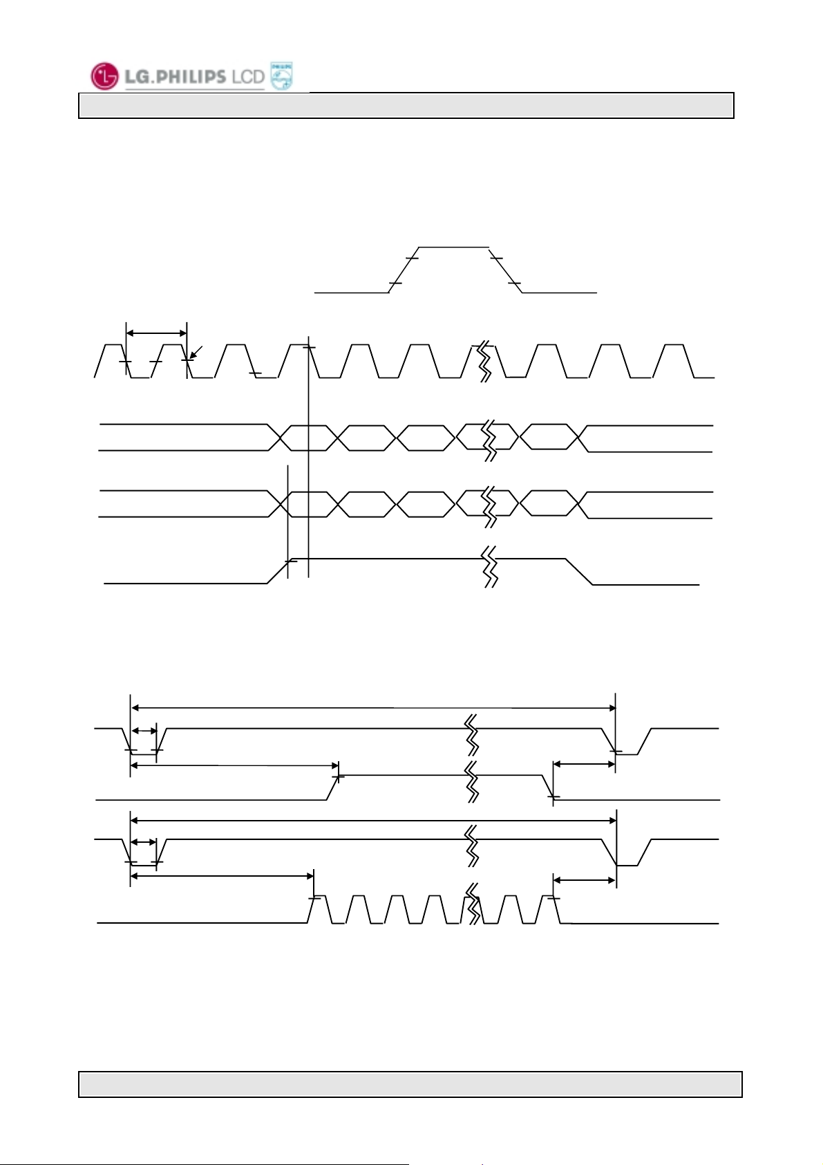
3-3. Signal Timing Specification
This is the signal tim ing r equired at the input of the LVDS T r ans mitter. All of the inter f ac e s ignal timing
should be satisfied with the following specifications for it’s proper operation.
Table 6. Timing Table
ITEM SYMBOL MIN. TYP. MAX. UNIT NOTE
Dclk Period t
Period t
Hsync
Width t
Period t
Vsync
Period t
Width t
DE
Horizontal
( Data
Back Porch
Enable )
Horizontal
Active
Horizontal
Front Porch
Vertical
Back Porch
Vertical
Active
Vertical
Front Porch
20.00 18.52 18.18 ns 1
730 844 -
856-
- 16.67 -
1032 1066 -
23-
12 124 -
t
CLK
HP
WH
VP
VP
WV
HBP
- - 640 -
t
t
HFP
VBP
624-
138-
- - 1024 -
t
VFP
11-
t
t
t
t
t
CLK
ms
HP
CLK
HP
HP
Note 1. Two pixel data are sampled at the same time.
Pixel
0,0
Pixel
0,1
Pixel
0,1023
Pixel
1,0
Pixel
1,1
Pixel
1,1023
pixel
2,0
pixel
2,1
pixel
2,1023
pixel
3,0
pixel
3,1
pixel
3,1023
1278,0
1278,1
1278,1023
Ver 1.0 SEP 30, 2000 Page 9/24
pixel
pixel
pixel
pixel
1279,0
pixel
1279,1
pixel
1279,1023
Page 10
3-4. Signal Timing Wave Form
,
Hsync,
Hsync, Vsync, DE, DATA
Hsync, Hsync,
tttt
CLK
CLK
CLKCLK
DCLK
DCLK
DCLKDCLK
INVALID
INVALID
INVALIDINVALID
First DATA
First DATA
First DATAFirst DATA
INVALID
INVALID
INVALIDINVALID
Second DATA
Second DATA
Second DATASecond DATA
Vsync, DE, DATA
Vsync, DE, DATAVsync, DE, DATA
0.5V
0.5V
0.5V0.5V
CC
CC
CCCC
pixel pixel
pixel pixel
1,0 3,0
Product Specification
0.7Vcc
0.7Vcc
0.7Vcc0.7Vcc
0.3Vcc
0.3Vcc
0.3Vcc0.3Vcc
VALID DATA
VALID DATA
VALID DATAVALID DATA
0
0 2,0
VALID DATA
VALID DATA
VALID DATAVALID DATA
LM157E2-
A2
INVALID
INVALID
INVALIDINVALID
INVALID
INVALID
INVALIDINVALID
DE(Data Enable)
DE(Data Enable)
DE(Data Enable)DE(Data Enable)
HSync
HSync
HSyncHSync
DE
DE
DEDE
tttt
WH
WH
WHWH
tttt
VSync
VSync
VSyncVSync
DE
DE
DEDE
tttt
HP
HP
HPHP
tttt
HBP
HBP
HBPHBP
tttt
VP
VP
VPVP
tttt
VBP
VBP
VBPVBP
tttt
HFP
HFP
HFPHFP
tttt
VFP
VFP
VFPVFP
Ver 1.0 SEP 30, 2000 Page 10/24
Page 11

LM157E2-
A2
Product Specification
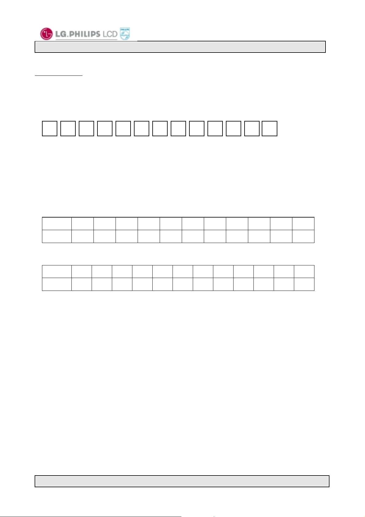
3-5. Color Input Data Reference
The brightness of each primary color(red, gr een and blue) is based on the 8-bit gray scale data input for
the color; the higher the binary input, the brighter the color. The table below provides a reference for
color versus data input.
Table 7. COLOR DATA REFERENCE
Input Color Data
Basic
Colors
Color
Black
Red(255)
Green(255)
Blue(255)
Cyan
Magenta
Yellow
White
Red
MSB LSB
R7 R6 R5 R4 R3 R2 R1 R0 G7 G6 G5 G4 G3 G2 G1 G0 B7 B6 B5 B4 B3 B2 B1 B0
0
0
0
0
0
0
1
1
1
1
1
1
0
0
0
0
0
0
0
0
0
0
0
0
0
0
0
0
0
0
1
1
1
1
1
1
1
1
1
1
1
1
1
1
1
1
1
1
MSB LSB
0
0
0
1
1
0
0
0
1
0
0
0
0
0
1
1
1
0
1
1
1
1
1
1
Green
MSB LSB
0
0
0
0
0
0
0
0
0
0
0
0
0
0
0
0
0
0
1
1
1
1
1
1
1
0
0
0
0
0
0
0
0
0
1
1
1
1
1
1
1
1
1
1
1
0
0
0
0
0
0
0
1
1
1
1
1
1
1
1
1
0
0
1
1
1
1
1
1
1
1
1
Blue
0
0
0
0
0
0
0
0
0
0
0
0
1
1
1
1
1
1
1
1
1
1
1
1
0
0
0
0
1
1
1
1
0
0
0
0
0
0
1
1
1
1
1
1
0
0
1
1
Red
Green
Blue
Red(000) Dark
Red(001)
Red(002)
Red(253)
Red(254)
Red(255) Bright
Green(000)Dark
Green(001)
Green(002)
Green(253)
Green(254)
Green(255)Bright
Blue(000) Dark
Blue(001)
Blue(002)
Blue(253)
Blue(254)
Blue(255) Bright
0
0
0
0
0
0
0
0
0
0
0
0
0
0
0
0
0
0
0
0
0
0
0
0
0
0
0
0
0
0
0
1
0
0
0
0
0
0
0
0
0
0
0
0
0
0
0
0
0
0
0
0
0
0
1
0
0
0
0
0
0
0
0
0
0
0
0
0
0
0
0
0
:
:
:
:
:
:
:
:
:
:
:
:
:
:
:
:
:
:
:
:
:
:
:
:
1
1
1
1
1
1
0
1
0
0
0
0
0
0
0
0
0
0
0
0
0
0
0
0
1
1
1
1
1
1
1
0
0
0
0
0
0
0
0
0
0
0
0
0
0
0
0
0
1
1
1
1
1
1
1
1
0
0
0
0
0
0
0
0
0
0
0
0
0
0
0
0
0
0
0
0
0
0
0
0
0
0
0
0
0
0
0
0
0
0
0
0
0
0
0
0
0
0
0
0
0
0
0
0
0
0
0
0
0
0
0
1
0
0
0
0
0
0
0
0
0
0
0
0
0
0
0
0
0
0
0
0
0
0
1
0
0
0
0
0
0
0
0
0
:
:
:
:
:
:
:
:
:
:
:
:
:
:
:
:
:
:
:
:
:
:
:
:
0
0
0
0
0
0
0
0
1
1
1
1
1
1
0
1
0
0
0
0
0
0
0
0
0
0
0
0
0
0
0
0
1
1
1
1
1
1
1
0
0
0
0
0
0
0
0
0
0
0
0
0
0
0
0
0
1
1
1
1
1
1
1
1
0
0
0
0
0
0
0
0
0
0
0
0
0
0
0
0
0
0
0
0
0
0
0
0
0
0
0
0
0
0
0
0
0
0
0
0
0
0
0
0
0
0
0
0
0
0
0
0
0
0
0
0
0
0
0
1
0
0
0
0
0
0
0
0
0
0
0
0
0
0
0
0
0
0
0
0
0
0
1
0
:
:
:
:
:
:
:
:
:
:
:
:
:
:
:
:
:
:
:
:
:
:
:
:
0
0
0
0
0
0
0
0
0
0
0
0
0
0
0
0
1
1
1
1
1
1
0
1
0
0
0
0
0
0
0
0
0
0
0
0
0
0
0
0
1
1
1
1
1
1
1
0
0
0
0
0
0
0
0
0
0
0
0
0
0
0
0
0
1
1
1
1
1
1
1
1
Ver 1.0 SEP 30, 2000 Page 11/24
Page 12
3-6. Power Sequences
Power Supply For LCD
V
CC
0V
0V
0V0V
Product Specification
90%
90%
90%90%
0%
0%0%
TTTT
2222
TTTT
LM157E2-
A2
90%
90%
90%90%
0%
0%0%
0%0%
TTTT
7777
TTTT
6666
TTTT
5555
Interface Signal,
Valid
Valid
V
i
ValidValid
(LVDS Signal of Transmitter)
0V
0V
0V0V
TTTT
3333
OFF
Power for Lamp
Parameter
T
1
T
2
T
3
T
4
T
5
T
6
T
7
OFF LAMP ON
OFFOFF
Values
Min. Typ. Max.
-
0.01
200
200
0.01
0.01
3
-
-
-
-
-
-
-
LAMP ON
LAMP ONLAMP ON
10
50
-
20
10
-
Units
ms
ms
ms
ms
ms
ms
s
Notes: 1. Please avoid floating state of interface signal at invalid period.
2. When the interface signal is invalid, be sure to pull down the power supply for LCD V
Invalid input with Vcc for a long time, cause permanent damage to LCD panel.
3. Lamp power must be turn on after power supply for LCD and interface signal are valid.
TTTT
4444
OFF
OFF
OFFOFF
to 0V.
CC
Ver 1.0 SEP 30, 2000 Page 12/24
Page 13
LM157E2-
A2
Product Specification
4. Optical Specifications
Optical characteristics are determined after the unit has been ‘ON’ and stable for approximately 30
minutes in a dark environm ent at 25. The values specified are at an approximate distanc e 50cm f rom
the LCD surface at a viewing angle of Φ and θ equal to 0°.
Appendix A -1 presents additional information concerning the measurement equipment and method..
Table 8. OPTICAL CHARACTERISTICS
Parameter Symbol
Min. Typ. Max.
Contrast Ratio CR 200 250 - - 1
Surface Luminance, white L
Luminance Variation
Response Time
Rise Time
Decay Time
WH
WHITE
Tr
Tr
R
Tr
D
170 200 - cd/m
-
-
CIE Color Coordinates
Red
Green
Blue
White
x
R
y
R
x
G
y
G
x
B
y
B
x
W
y
W
0.602
0.321
0.282
0.546
0.120
0.086
0.283
0.299
Values
6
19
0.632
0.351
0.312
0.576
0.150
0.116
0.313
0.329
Units Notes
2
1.30 - 3
15
msec
30
0.662
0.381
0.342
0.606
0.180
0.146
0.342
0.359
2
4
Viewing Angle
x axis, right (=0º)
x axis, left(=180º)
y axis, up(=90º)
y axis, down (=270º)
x
x
y
y
+60
-60
+45
-45
-
-
-
-
Degree
Gamma Value(reference value) 2.6 6
Crosstalk 2.5 % 7
Flicker -23 -20 dB 8
Notes 1. Contrast Ratio (CR) is defined mathematically as :
Surface Luminance with all white pixels
Contrast Ratio =
Surface Luminance with all black pixels
Surface Luminance with all black pixels
Surface Luminance with all black pixels Surface Luminance with all black pixels
2. Surface luminance is the center point across the LCD surf ace 50cm from the surface with all
pixels displaying white. For more information see Appendix A - 2.
3. The variation in surface Luminance,
position 1 through 5, and then dividing the max imum L
of 5 points luminance. For more information see Appendix A - 2.
L
ON
Maximum (L
WHITE
ON1
, L
is determined by measuring LON at each test
WHITE
of 5 points luminance by minim um
ON
ON2
, ....L
) Minimum (L
ON5
ON1
, L
ON2
, ....L
ON5
5
)
Ver 1.0 SEP 30, 2000 Page 13/24
Page 14

LM157E2-
((
A2
Product Specification
4. Response time is the time r equired for the display to transition from blac k to white (Rise Tim e,
) and from white to black (Decay Time, TrD). For additional information see Appendix A - 3.
Tr
R
5. Viewing angle is the angle at which the contrast ratio is greater than 10. The angles are
determined for the horizontal or x axis and the ver tical or y axis with res pect to the z axis which is
normal to the LCD surface. For more information see Appendix A - 4
6.Gray scale specification is as following.
Gray Level
L0 0.01
L31 0.37
L63 0.98
L95 3.93
L127 9.60
L159 19.5
L191 39.7
L223 62.7
L255 100
7. Cross talk shall be measured at the V and H position.(Window size : 256 x 204 pixels)
For more information see Appendix A-5
Crosstalk Ratio =
Luminance at Pattern A - Luminance at pattern B
Luminance
(%)(min)
Luminance at pattern B
Luminance
(%)(typ)
0.26 0.51
0.97 1.57
2.48 3.98
6.83 9.73
14.8 20.2
29.3 39.1
51.0 62.3
72.9 83.1
100 100
Luminance
(%)(max)
×
100(%)
8. Flicker shall be measured at the center location.
Test pattern : Pixel pattern
Background RGB gray(0, 0, 0)
Foreground RGB gray(127, 127, 127)
AC at
(
5. Mechanical Characteristics
Ver 1.0 SEP 30, 2000 Page 14/24
Test
=
=
= =
20 log
(
DC level
Page 15

LM157E2-
A2
Product Specification
The chart below provides general mechanical characteristics for the model LM157E2-A2 LCD. In
addition, the figure below is a detailed mechanical drawing of the LCD. Note that dimensions are given for
reference purposes only.
Parameters Value unit Notes
Outside dimensions
Horizontal
Vertical
Depth
Bezel area
Horizontal
Vertical
Active Display area
Horizontal
Vertical
Weight 1140(typ) gram -
335
273.5
11.2
314.2
252.0
311.040
248.832
mm -
mm -
mm -
Surface Treatment
Hard coating 3H.
Anti-glare treatment of the
front polarizer
--
Ver 1.0 SEP 30, 2000 Page 15/24
Page 16

< FRONT VIEW >
LM157E2-
A2
Product Specification
Ver 1.0 SEP 30, 2000 Page 16/24
Page 17

Product Specification
LM157E2-
A2
Ver 1.0 SEP 30, 2000 Page 17/24
Page 18

< REAR VIEW >
6. Reliability
- Environment test condition
No. Test ITEM Conditions
1 High temperature storage test Ta = 60 240h
2 Low temperature storage test Ta = -20 240h
3 High temperature operation test Ta = 50 50%RH 240h
4 Low temperature operation test Ta = 0 240h
5 Humidity Condition operation 20%RH ~ 80%RH
6 Humidity Condition storage 5%RH ~ 90%RH
Vibration test
7
(non-operating)
Shock test
8
(non-operating)
LM157E2-
A2
Product Specification
Wave Form: Random
Vibration Level: 1.0Grms
Bandwidth: 10~500Hz
Duration: 20min/Axis(X,Y,Z)
One time each direction
Shock Level: 120G
Wave Form: Half Sine Wave, 2ms
Direction: X, Y, Z,
One time each direction
Altitude
9
storage/shipment 0 - 53,300 feet
{Result Evaluation Criteria}
There should be no change which might affect the practical display function when the display quality
test is conducted under normal operating condition.
Ver 1.0 SEP 30, 2000 Page 18/24
Page 19

LM157E2-
A2
Product Specification
7. International Standards
7-1. Safety
a) UL 1950 Third Edition, Underwriters Laboratories, Inc. Jan. 28, 1995.
Standard for Safety of Information Technology Equipment Including Electrical Business
Equipment.
b) CAN/CSA C22.2 No. 950-95 Third Edition, Canadian Standards Association, Jan. 28, 1995.
Standard for Safety of Information Technology Equipment Including Electrical Business
Equipment.
c) EN 60950 : 1992 + A1 : 1993 + A2 : 1993 + A3 : 1995 + A4 : 1997 + A11 : 1997
IEC 950 : 1991 + A1 : 1992 + A2 : 1993 + A3 : 1995 + A4 : 1996
European Committee for Electrotechnical Standardization (CENELEC)
EUROPEAN STANDARD for Safety of Information Technology Equipment Including Electrical
Business Equipment.
7-2. EMC
a) ANSI C63.4 “Methods of Measurement of Radio-Noise Emissions from Low-Voltage Electrical
and Electronic Equipment in the Range of 9kHz to 40GHz.” American National Standards
Institute(ANSI),1992.
b) C.I.S.P.R “Limits and Methods of Measurement of Radio Interference Characteristics of
Information Technology Equipment.” International Special Committee on Radio Interference
(standards apply by CISPR22 Class-B)
c) EN 55022 “Limits and Methods of Measurement of Radio Interference Characteristics of
Information Technology Equipment.” European Committee for Electrotechnical
Standardization (CENELEC),1988
Ver 1.0 SEP 30, 2000 Page 19/24
Page 20
8. Packaging
8-1. Designation of Lot Mark
a) Lot Mark
LM157E2-
A2
Product Specification
KJIHGFEDCBA L
A, B, C : INCH CODE
D : YEAR
E : MONTH
F, G : PANEL CODE
H : ASSEMBLY CODE
I, J, K, L, M : SERIAL NO.
Note : 1. YEAR
YEAR 96 97 98 99 2000 2001 2002 2003 2004 2005 2006
Mark67890123456
2. MONTH
MONTH Jan. Feb. Mar. Apr. May Jun. Jul. Aug. Sep. Oct. Nov. Dec.
Mark123456789ABC
b) Location of Lot Mark
MMMM
Serial NO. is printed on the label. The label is attached to the backside of the LCD module.
This is subject to change without prior notice.
8-2. Packing Form
a) Package quantity in one box : 8 pcs
b) Box Size : 344mm315mm410mm
Ver 1.0 SEP 30, 2000 Page 20/24
Page 21
LM157E2-
A2
Product Specification
9.PRECAUTIONS
Please pay attention to the followings when you use this TFT/LCD module.
9.1 MOUNTING PRECAUTIONS
(1) You must mount a module user holes arranged in four corners.
(2) You should consider the mounting structure so that uneven force (ex. twisted stress) is not applied
to the module.
And the case on which a module is mounted should have sufficient strength so that external
force is not transmitted directly to the module.
(3) Please attach the surface with a transparent protective plate in order to protect the polarizer LC cell.
Transparent protective plate should have sufficient strength in order to resist external force.
(4) You should adopt radiation structure to satisfy the temperature specification.
(5) Acetic acid type and chlorine type materials for the cover case are not desirable because the former
generates corrosive gas of attacking the polarizer at high temperature and the latter causes circuit
break by electro-chemical reaction.
(6) Do not touch, push or rub the exposed polarizer with glass, tweezers or anything harder than HB
pencil head And Please do not rub with dust clothes with chemical treatment.
Do not touch the surface of polarizer for bare hand or greasy cloth. (Some cosmetics are
detrimental to the polarizer.)
(7) When the surface becomes dusty, please wipe gently with absorbent cotton or other soft materials
like chamois soaked with petroleum benzene. Normal-hexane is recommended for cleaning the
adhesives used to attach front / rear polarizer. Do not use acetone, toluene and alcohol because
they cause chemical damage to the polarizer.
(8) Wipe off saliva or water drops as soon as possible. Their long time contact with polarizer causes
deformations and color fading.
(9) Do not open the case because inside circuits do not have sufficient strength.
9.2 OPERATING PRECAUTIONS
(1) The spike noise causes the malfunction of circuits. It should be lower than following voltage :
V = ± 200mV (Over and under shoot voltage).
(2) Response time depends on the temperature. (In lower temperature, it becomes longer.)
(3) Brightness depends on the temperature. (In lower temperature, it becomes lower.)
And in lower temperature, response time (required time that brightness is stable after turned on )
becomes longer.
(4) Be careful for condensation at sudden temperature change. Condensation makes damage to
polarizer or electrical contacted parts. And after fading condensation, smear or spot will occur.
(5) When fixed patterns are displayed for a long time, remnant image is likely to occur.
(6) A module has high frequency circuit. If you need to shield the electromagnetic noise, please do
co-work together.
9.3 ELECTROSTATIC DISCHARGE CONTROL
Since a module is com posed of electronic circuits. it is not strong to electrostatic discharge. Mak e
certain that treatment pers ons are connected to ground through wrist band etc. . . And don’t touch
I/F pin directly.
9.4 PRECAUTION FOR STRONG LIGHT EXPOSURE
Strong light exposure causes degradation of polarizer and color filter.
9.5 STORAGE
When storing modules as spares for a long time. The following precautions are necessary.
(1) Store them in a dark place. Do not expose the module to sunlight or fluorescent light. Keep the
temperature between 5 and 35 at normal humidity.
(2) The polarizer surface should not come in contact with any other object.
It is recommended that they be stored in the container in which they were shipped.
Ver 1.0 SEP 30, 2000 Page 21/24
Page 22

LM157E2-
A2
Product Specification
9.6 HANDLING PRECAUTIONS FOR PROTECTION FILM
(1) When the protection film is peeled off, static electricity is generated between the film and polarizer.
This should be peeled off slowly and carefully by people who are electrically grounded and with well
ion- blown equipment or in such a condition, etc..
(2) The protection film is attached to the polarizer with a small amount of adhesive tape. If some stress
is applied to rub the protection film against the polarizer during the time you peel off the film, the
adhesive tape is apt to remain on the polarizer.
Please carefully peel off the protection film without rubbing it against the polarizer.
(3) When the module with protection film attached is stored for a long time, sometimes there remains a
very small amount of adhesive tape still on the polarizer after the protection film is peeled off.
(4) You can remove the adhesive easily. When the adhesive remains on the polarizer surface or its
vestige is recognized, please wipe them off with absorbent cotton waste or other soft material like
chamois soaked with normal- hexane.
Ver 1.0 SEP 30, 2000 Page 22/24
Page 23
LM157E2-
Product Specification
APPENDIX
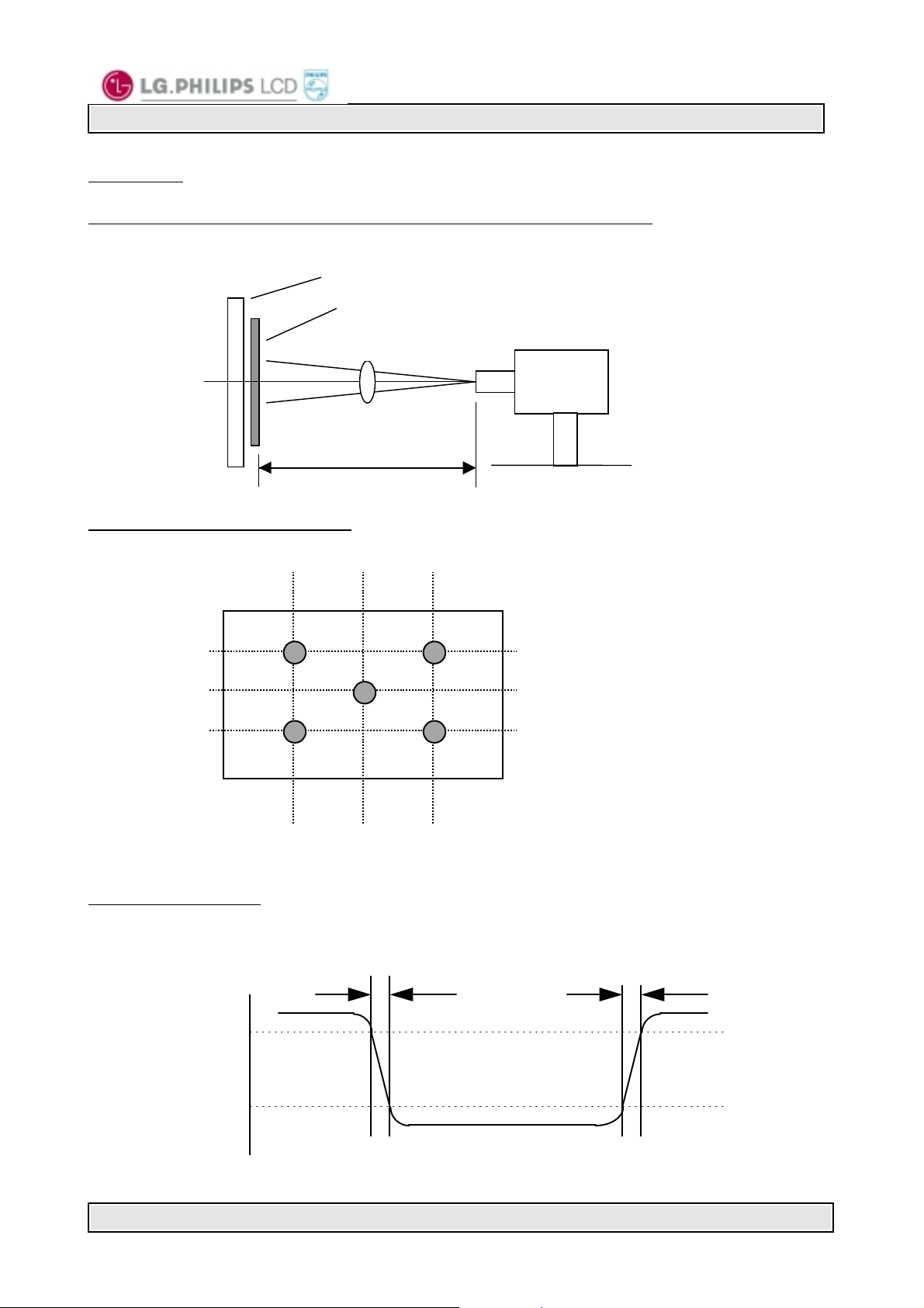
A-1 Optical Characteristic Measurement Equipment and Method
Optical Stage(x,y)
LCD Module
A2
A-2 Luminance Measurement
320
320320
2222
4444
Field =
500mm
640320
640640
°
960
960640
960960
Prichard PR-880 or
equivalent
256
256
3333
5555
256256
52
52
5252
768
768
768768
<Measuring point for luminance variation & surface luminance>
A-3 Response Time
The response time is defined as the following figure and shall be measured by switching
the input signal for “black” and “white”.
R
Tr
%
100
90
Optical
Response
10
Ver 1.0 SEP 30, 2000 Page 23/24
white
0
black
D
Tr
white
Page 24

A-4 Viewing angle
<Definition of viewing angle range>
Product Specification
θ
0
φ
90
2:00)
yu
z
θ
LM157E2-
A2
A
φ
φ
180
xl
9:00)
A-5 Crosstalk Measurement
: (
L
Crosstalk
(
L
A[or C]2-LA[or C]1
L
B[or D]2-LB[or D]1
, L
A[or C]1
B[or D]1
TFT LCD
MODULE
, L
/L
A[or C]1
/L
B[or D]1
, L
A[or C]2
A(640,128)
φ
0
3:00)
xr
φ
z' yd
)
100(%)[vertical],
××××
)
100(%)[horizontal]
××××
is luminance of pattern1,2 at position A, B, C, D
B[or D]2
270
6:00)
D(160,512)
Pattern 1
Background : Mid-gray
B(1120,512)
C(640,896)
Pattern 2
Window : Black/White
Background : Mid-gray
Window Size : 50%
Ver 1.0 SEP 30, 2000 Page 24/24
 Loading...