

Page 1
)
(
Preliminary Specification
●
)
(
Final Specification
LC470WUD
Product Specification
SPECIFICATION
FOR
APPROVAL
47.0” WUXGA TFT LCDTitle
MODEL
APPROVED BY
/
/
/
GeneralBUYER
SIGNATURE
DATE
LG Display Co., Ltd.SUPPLIER
LC470WUD*MODEL
SAB1(RoHS Verified)SUFFIX
*When you obtain standard approval,
please use the above model name without suffix
APPROVED BY
J.H.Lee / Team Leader
REVIEWED BY
P.Y. Kim / Project Leader
PREPARED BY
H.J.Kim / Engineer
SIGNATURE
DATE
Please return 1 copy for your confirmation with
your signature and comments.
Ver. 0.1
TV Product Development Dept.
LG Display Co., Ltd
1/ 38
Page 2
Product Specification
CONTENTS
LC470WUD
COVER
CONTENTS
GENERAL DESCRIPTION1
ABSOLUTE MAXIMUM RATINGS2
ELECTRICAL SPECIFICATIONS3
ELECTRICAL CHARACTERISTICS3-1
INTERFACE CONNECTIONS3-2
SIGNAL TIMING SPECIFICATIONS3-3
SIGNAL TIMING WAVEFORMS3-4
COLOR DATA REFERENCE3-5
POWER SEQUENCE3-6
OPTICAL SPECIFICATIONS4
MECHANICAL CHARACTERISTICS5
ITEMNumber
Page
1
2
3RECORD OF REVISIONS
4
5
6
6
8
11
12
13
14
16
20
Ver. 0.1
RELIABILITY6
INTERNATIONAL STANDARDS7
SAFETY7-1
EMC7-2
PACKING8
DESIGNATION OF LOT MARK8-1
PACKING FORM8-2
23
24
24
24
25
25
25
26PRECAUTIONS9
26MOUNTING PRECAUTIONS9-1
26OPERATING PRECAUTIONS9-2
27ELECTROSTATIC DISCHARGE CONTROL9-3
27PRECAUTIONS FOR STRONG LIGHT EXPOSURE9-4
27STORAGE9-5
27HANDLING PRECAUTIONS FOR PROTECTION FILM9-6
2/ 38
Page 3
Product Specification
RECORD OF REVISIONS
Preliminary Specification (First Draft) -June. 30, 20080.1
LC470WUD
DescriptionPageRevision DateRevision No.
Ver. 0.1
3/ 38
Page 4

LC470WUD
Product Specification
1. General Description
LC470WUD is a Color Active Matrix Liquid Crystal Display with anCold Cathode Fluorescent
Lamp(CCFL) backlight system. The matrix employs a-Si Thin Film Transistor as the active element.
It is a transmissive type display operating in the normally black mode. It has a 46.96 inch diagonally
measured active display area with WUXGA resolution (1080 vertical by 1920 horizontal pixel array)
Each pixel is divided into Red, Green and Blue sub-pixels or dots which are arranged in vertical stripes.
Gray scale or the luminance of the sub-pixel color is determined with a 10-bit gray scale signal for
each dot, thus presenting a palette of more than 1.07Billion of colors.
Ithas been designed to apply the 10-bit 4 port LVDS interface.
It is intended to support LCD TV, PCTV where high brightness, super wide viewing angle, high color gamut,
high color depth and fast moving picture response time are important.
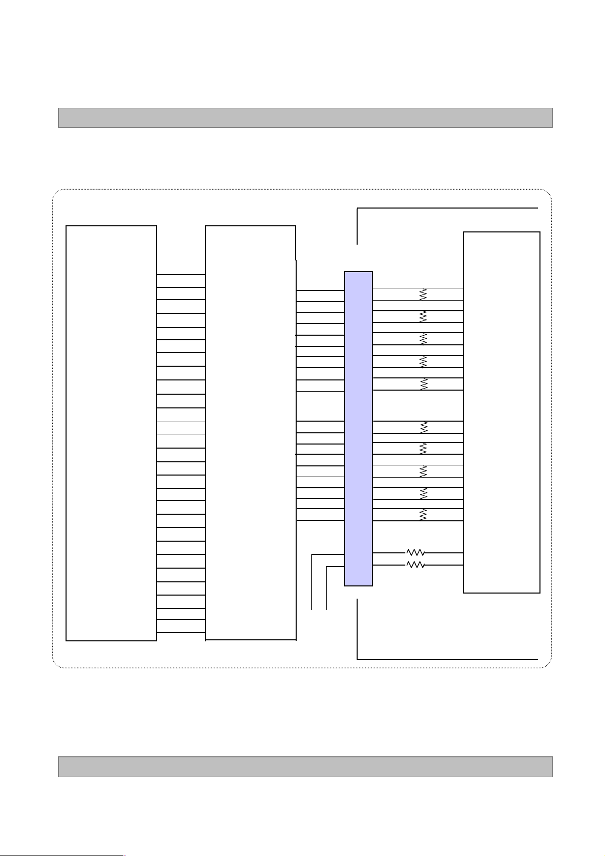
Mini-LVDS(RGB)
SDA
Source Driver Circuit
Gate Driver Circuit
S1S1920
G1
LVDS
2Port
CN2
(41pin)
LVDS 3,4
SDRAM
MEM
CTRL
RGB
EEPROM
SCL
+12.0V
LVDS
2Port
LVDS Selection
+24.0V, GND, VBR-A,VBR-B
CN1
(51pin)
+24.0V, GND
LVDS 1,2
Option
signal
I2C
General Features
Timing Controller
(ASIC)
Power Circuit
Block
Inverter(Master)
Inverter(Slave)
46.96 inch (1192.87mm) diagonalActive Screen Size
1096.0(H) x 640.0 (V) x 53.1 mm(D) (Typ.)Outline Dimension
0.5415 mm x 0.5415 mm x RGBPixel Pitch
1920 horiz. by 1080 vert. Pixels, RGB stripe arrangementPixel Format
10Bit , 1.07 Billion colorsColor Depth
500 cd/m2 (Center 1point ,Typ.)Luminance, White
TFT -LCD Panel
(1920 × RGB × 1080 pixels)
G1080
3PinX1CN(High)
Back light Assembly
3PinX1CN(High)
Ver. 0.1
Viewing angle free ( R/L 178 (Min.), U/D 178 (Min.))Viewing Angle (CR>10)
Total 221.22 W (Typ.) [Logic=8.22W, Backlight=213W (VBR-A=1.65V)]Power Consumption
14.5 Kg (Typ.) Weight
Transmissive mode, Normally blackDisplay Mode
Hard coating(3H), Anti-glare treatment of the front polarizer (Haze 13%)Surface Treatment
4/ 38
Page 5
LC470WUD
Product Specification
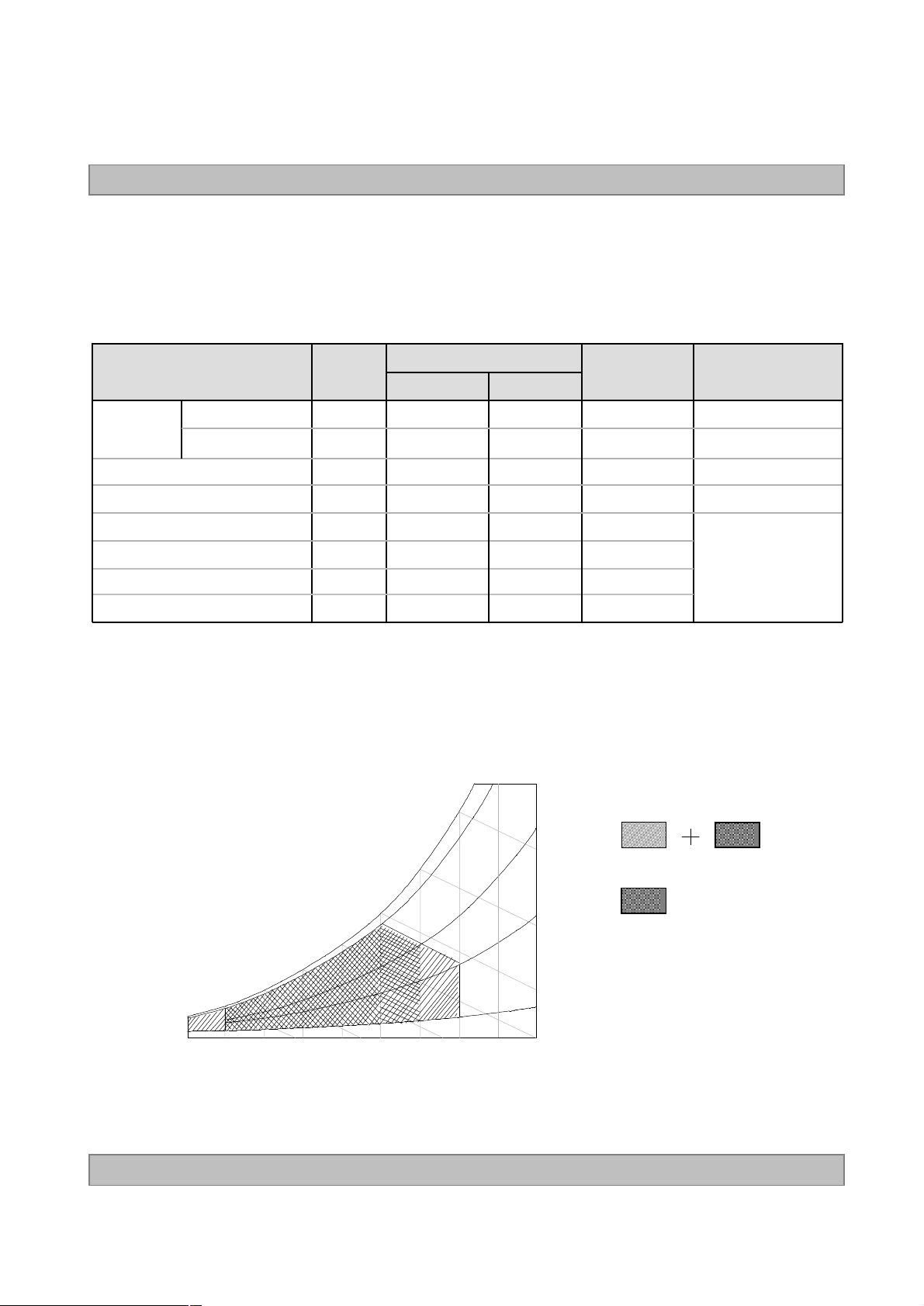
2. Absolute Maximum Ratings
The following items are maximum values which, if exceeded, may cause faulty operation or damage to the
LCD module.
Table 1. ABSOLUTE MAXIMUM RATINGS
Value
Parameter Remark
Symbol
Unit
MaxMin
Power Input
Voltage
LCM
VDC+27.0-0.3VBLBacklight inverter
VDC+5.5-0.3VON/OFFON/OFF Control Voltage
VDC+5.00VBRBrightness Control Voltage
+500TOPOperating Temperature
+60-20TSTStorage Temperature
°C
°C
%RH9010HOPOperating Ambient Humidity
%RH9010HSTStorage Humidity
Note : 1. Temperature and relative humidity range are shown in the figure below.
Wet bulb temperature should be 39 °C Max. and no condensation of water.
2. Gravity mura can be guaranteed under 40°C condition.
90%
60
60%
at 25 ± 2 °CVDC+14.0-0.3VLCD
Note 1,2
Ver. 0.1
Wet Bulb
Temperature [°C]
20
10
0
10203040506070800-20
Dry Bulb Temperature [°C]
30
40
50
40%
10%
Storage
Operation
Humidity [(%)RH]
5/ 38
Page 6
Product Specification
3. Electrical Specifications
3-1. Electrical Characteristics
It requires two power inputs. One is employed to power for the LCD circuit.
The other Is used for the CCFL backlight circuit.
Table 2. ELECTRICAL CHARACTERISTICS
LC470WUD
Parameter Symbol
Value
Circuit :
Power Input Voltage
Power Input Current
Power Consumption
Rush current
LCD
I
LCD
LCD
RUSH
Notes: 1. The specified current and power consumption are under the V
condition whereas mosaic pattern(8 x 6) is displayed and fVis the frame frequency.
2. The current is specified at maximum current pattern.
3. The duration of rush current is about 2ms and rising time ofpower input is 0.5ms (min.).
White : 1023 Gray
Black : 0 Gray
MaxTypMin
12.612.011.4V
=12.0V, 25 ± 2°C, fV=120Hz
LCD
V
DC
NoteUnit
1mA891685479
2mA1235950665
1Watt10.6868.22-P
3A5--I
Ver. 0.1
Mosaic Pattern(8 x 6)
6/ 38
Page 7
Product Specification
Table 3. ELECTRICAL CHARACTERISTICS for IPB& Lamp (Continue)
LC470WUD
Parameter Symbol
Inverter :
Power Supply
Input Current
Power Consumption
Input Voltage for
Control System
Signals
Lamp:
On/Off
OnVdc5.0-2.5V on
Off
Brightness Adjust
Values
NotesUnit
MaxTypMin
Vdc25.224.022.8VBLPower Supply Input Voltage
1
1Vp-p0.5--Power Supply Input Voltage Ripple
8.8-
10.3
VBR-A = 1.65V … 1A
IBL_AAfter Aging
10.0-
11.0-
11.0
12.0
VBR-A = 3.3V … 1A
VBR-A = 1.65V … 2A
IBL_BBefore Aging
12.0-
13.0
VBR-A = 3.3V … 2A
VBL = 22.8V
VBR-B = 3.3V
A14.0--IrushPower Supply Input Current (In-Rush)
VBR-A = 1.65V
-PBL
250213
VBR-A = 1.65V … 1W
Vdc3.31.650.0VBR-ABrightness Adjust
Vdc0.80.0-0.3V off
V3.3-0VBR-B
3min3Ts
4Hrs30,000Life Time
Notes :
1. Electrical characteristics are determined after the unit has been ‘ON’ and stable for approximately 120
minutes at 25±2°C. The specified current and power consumption are under the typical supply Input voltage
24Vand VBR (VBR-A : 1.65V & VBR-B :100%), it is total power consumption.
The ripple voltage of the power supply input voltage is under 0.5 Vp-p. LPL recommend Input Voltage is
24.0V ± 5%.
2. Electrical characteristics are determined within 30 minutesat 25±2°C.
The specified currents are under the typical supply Input voltage 24V.
3. The brightness of the lamp after lighted for 5minutes is defined as 100%.
TS is the time required for the brightness of the center of the lamp to be not less than 95% at typical current.
The screen of LCD module may be partially dark by the time the brightness of lamp is stable after turn on.
4. Specified Values are for a single lamp which is aligned horizontally.
The life time is determined as the time which luminance ofthe lamp is 50% compared to that of initial value
at the typical lamp current (VBR-A : 1.65V & VBR-B :3.3V), on condition of continuous operating at 25± 2°C
5. The duration of rush current is about 10ms.
Ver. 0.1
7/ 38
Page 8
LC470WUD
Product Specification
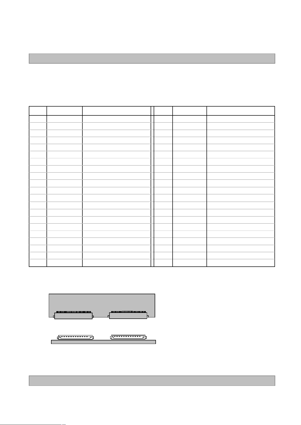
3-2. Interface Connections
This LCD module employs two kinds of interface connection, 51pin(CN1) and 41pin(CN2) connectors are
used for the module electronics two 3-pin Balance PCB connectors are used for the integral backlight system.
3-2-1. LCD Module
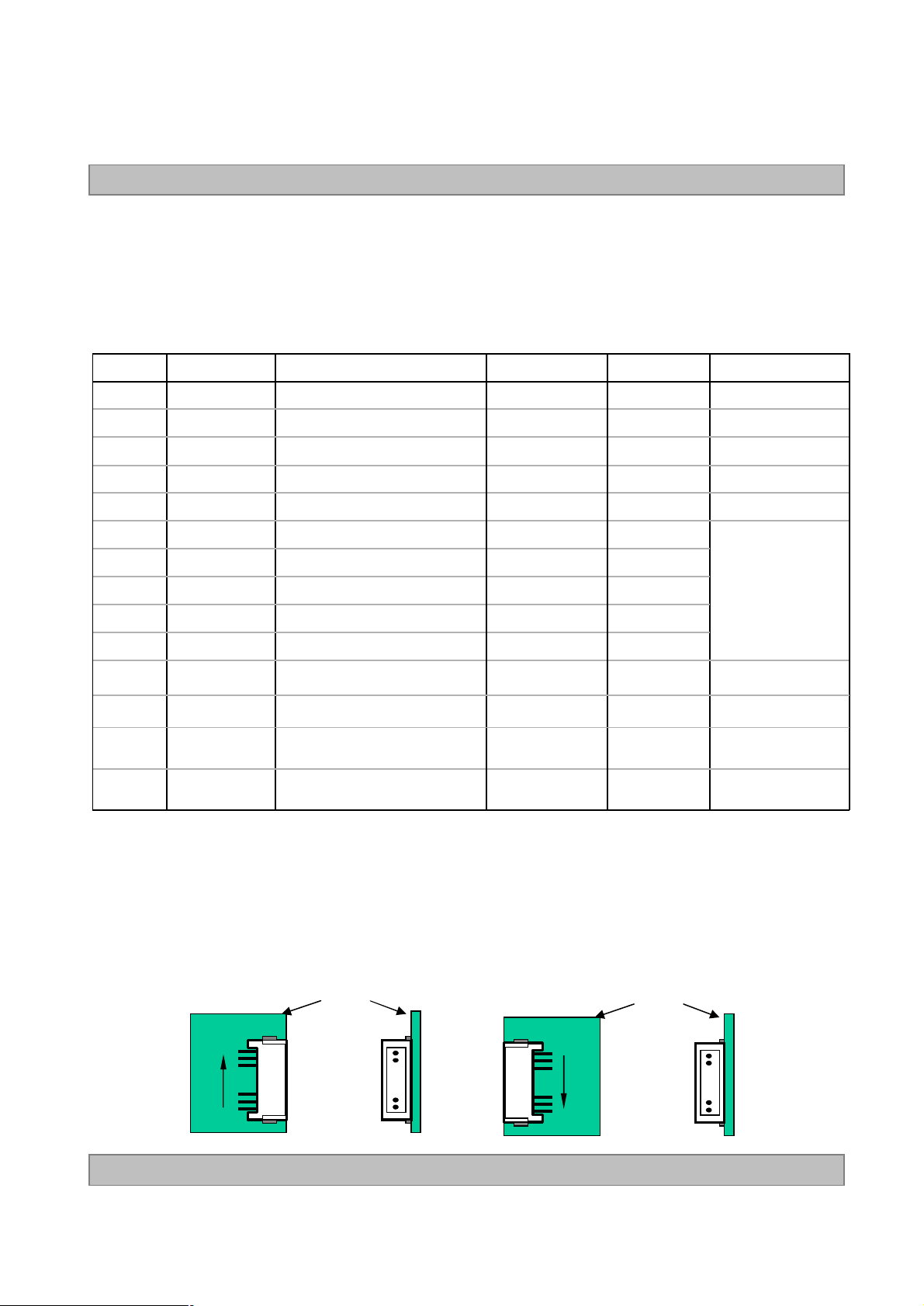
-LCD Connector(CN1): FI-RE51S-HF or Equivalent, Refer to below table.
-Mating Connector : FI-RE51HL
Table 4-1. MODULE CONNECTOR(CN1) PIN CONFIGURATION
10
11
12
13
14
16
17
18
19
21
22
23
24
25
26
DescriptionSymbolNo
GND
2
3
5
6
8
9
NC
NC
NC
NC
NC
NC
NC
GND
RA1N
RA1P
RB1N
RC1N
RC1P
GND
RCLK1N
GND
RD1N
RD1P
RE1N
RE1P
GND
Ground1
Reserved
Reserved
ReservedNC4
Reserved
Reserved
‘‘H’ =JEIDA , ‘L’ = VESA LVDS Select7
Reserved
Reserved
Reserved
Ground
FIRST CHANNEL AFIRST CHANNEL A+
FIRST CHANNEL BFIRST CHANNEL B+RB1P15
FIRST CHANNEL CFIRST CHANNEL C+
Ground
FIRST CLOCK CHANNEL ClkFIRST CLOCK CHANNEL Clk+RCLK1P20
Ground
FIRST CHANNEL DFIRST CHANNEL D+
FIRST CHANNEL E-
FIRST CHANNEL E+
Ground
No
27
28
29
30
31
32
33
34
35
36
37
38
39
40
41
42
43
44
45
46
47
48
49
50
51
-
Symbol
NC
RA2N
RA2P
RB2N
RB2P
RC2N
RC2P
GND
RCLK2N
RCLK2P
GND
RD2N
RD2P
RE2N
RE2P
GND
GND
GND
GND
GND
NC
VLCD
VLCD
VLCD
VLCD
-
NC
SECOND CHANNEL ASECOND CHANNEL A+
SECOND CHANNEL BSECOND CHANNEL B+
SECOND CHANNEL CSECOND CHANNEL C+
Ground
SECOND CLOCK CHANNEL ClkSECOND CLOCK CHANNEL Clk+
Ground
SECOND CHANNEL DSECOND CHANNEL D+
SECOND CHANNEL ESECOND CHANNEL E+
Ground
Ground
Ground (NSB)
Ground
Ground
No connection
Power Supply +12.0V
Power Supply +12.0V
Power Supply +12.0V
Power Supply +12.0V
Description
-
Notes : 1. All GND(ground) pins should be connected together to the LCD module’s metal frame.
2. All VLCD (power input) pins should be connected together.
3. All Input levels of LVDS signals are based on the EIA 664 Standard.
4. Specific pins(pin No. #2~#6) are used for internal data process of the LCD module.
If not used, these pins are no connection.
5. Specific pins(pin No. #8~#9) are used for Inverter test of the LCD module.
If not used, these pins are no connection.
6. Specific pin No. #44 is used for “No signal detection” of system signal interface.
It should be GND for NSB(No Signal Black) during the system interface signal is not.
If this pin is “H”, LCD Module displays AGP(Auto Generation Pattern).
Ver. 0.1
8/ 38
Page 9
Product Specification
-LCD Connector(CN2): FI-RE41S-HF or Equivalent, Refer to below table
-Mating Connector : FI-RE41HL
Table 4-2. MODULE CONNECTOR(CN2) PIN CONFIGURATION
LC470WUD
10
11
12
14
15
16
17
19
20
21
DescriptionSymbolNo
NC
2
3
5
6
7
8
9
NC
NC
NC4
NC
NC
NC
NC
GND
RA3N
RA3P
RB3N
RB3P13
RC3N
RC3P
GND
RCLK3N
RCLK3P18
GND
RD3N
RD3P
No connection(Reserved)1
No connection
No connection
No connection
No connection
No connection
No connection
No connection
Ground
Third CHANNEL A-
Third CHANNEL A+
Third CHANNEL BThird CHANNEL B+
Third CHANNEL CThird CHANNEL C+
Ground
Third CLOCK CHANNEL Clk-
Third CLOCK CHANNEL Clk+
Ground
Third CHANNEL DThird CHANNEL D+
No
22
23
24
25
26
27
28
29
30
31
32
33
34
35
36
37
38
39
40
41
-
Symbol
RE3N
RE3P
GND
GND
RA4N
RA4P
RB4N
RB4P
RC4N
RC4P
GND
RCLK4N
RCLK4P
GND
RD4N
RD4P
RE4N
RE4P
GND
GND
Third CHANNEL EThird CHANNEL E+
Ground
Ground
Fourth CHANNEL AFourth CHANNEL A+
Fourth CHANNEL BFourth CHANNEL B+
Fourth CHANNEL CFourth CHANNEL C+
Ground
Fourth CLOCK CHANNEL Clk-
Fourth CLOCK CHANNEL Clk+
Ground
Fourth CHANNEL DFourth CHANNEL D+
Fourth CHANNEL EFourth CHANNEL E+
Ground
Ground
Description
Note : 1. All GND(ground) pins should be connected together to the LCD module’s metal frame.
[CN1]
CN1 CN2
#1
#51#1#41
-Part/No. : FI-RE51S-HF(JAE)
-Mating connector : FI-RE51HL
(Manufactured by JAE)
[CN2]
#1#51
#1#41
-Part/No. : FI-RE41S-HF(JAE)
-Mating connector : FI-RE41HL
(Manufactured by JAE)
Rear view of LCM
Ver. 0.1
9/ 38
Page 10
Product Specification
3-2-2. Backlight Inverter
Master
-Inverter Connector : S14B-PH-SMC (JST)
or Equivalent
-Mating Connector : PHR-14 or Equivalent
Table 5. INVERTER CONNECTOR PIN CONFIGULATION
LC470WUD
Slave
-Inverter Connector : S12B-PH-SMC (JST)
or Equivalent
-Mating Connector : PHR-12 or Equivalent
Master
Slave
NoteDescriptionSymbolPin No
1
2
3
4
5
6
7
8
9
10
11
12
13
14
VBR-A
ON/OFF
V
VBR-B
GND
Power Supply +24.0VV BL
Power Supply +24.0VV BL
Power Supply +24.0VV BL
Power Supply +24.0VV BL
Power Supply +24.0VV BL
Backlight GroundGND
Backlight GroundGND
Backlight GroundGND
Backlight GroundGND
Backlight GroundGND
Analog dimming voltage
DC 0.0V ~ 3.3V (Typ : 1.65V)
0.0V ~ 5.0V
Burst dimming voltage
DC 0.0V ~ 3.3V
Normal : Upper 3.0V
Abnormal : Under 0.7V
VBL
VBL
VBL
VBL
VBL
GND
GND
GND
GND
GND
VBR-B
Notes : 1. GND should be connected to the LCD module’s metal frame.
2. If Pin #11 is open, VBR-A = 1.65V. When apply over 1.65V( ~ 3.3V) continuously,
its luminance is increasing however lamp’s life time is decreasing.
It could be usable for boost up luminance when using DCR (=Dynamic contrast ratio) function only.
3. Minimum Brightness : VBR-B =0V Maximum Brightness : VBR-B = 3.3V
4. Even though Pin #14 is open, there is no effecton inverter operating, The output terminal of inverter.
5. Each impedance of pin #11,12 and 13 is 143[KΩ], 41[KΩ],105[KΩ]
Don’t careOn/Off
VBL
VBL
VBL
VBL
VBL
GND
GND
GND
GND
GND
-
1
2, 3Don’t careVBR-A
3
4-Status
◆ Rear view of LCM
14
1
Ver. 0.1
…
<Master>
PCB
…
PCB
1
…
…
12
<Slave>
10/ 38
Page 11
LC470WUD
Product Specification
3-3. Signal Timing Specifications
Table 6 shows the signal timing required at the input of the LVDS transmitter. All of the interface signal timing
should be satisfied with the following specification for normal operation.
Table 6. TIMING TABLE for NTSC/ATSC (DE Only Mode)
Symbol
Display Period
Horizontal
Blank
Total
Display Period
VerticalLines864510
Blank
Total
tHV
tHB
tHP
tVV
tVB
tVP
Symbol
fCLK
fH
fV
Frequency
DCLK
Horizontal
Vertical
tclk2007040
tclk680550520
Lines-1080-
Lines116611251090
75.0074.2566.97
136.4135121.8
121.2120108.2
MHz
KHz
Hz
NotesUnitMaxTypMinITEM
1920/4tclk-480-
NotesUnitMaxTypMinITEM
Table 7 shows the signal timing required at the input of the LVDS transmitter. All of the interface signal timing
should be satisfied with the following specification for normal operation.
Table7. TIMING TABLE for DVB/PAL (DE Only Mode)
Display Period
Symbol
tHV
-480-
tclk
NotesUnitMaxTypMinITEM
1920/4
Horizontal
Vertical
Frequency
Blank
Total
Display Period
Blank
Total
DCLK
Horizontal
Vertical
tHB
tHP
tVV
tVB
tVP
Symbol
fCLK
fH
fV
2007040
680550520
-1080-
300270228
138013501308
75.0074.2566.97
136.4135121.8
103.710095
tclk
tclk
Lines
Lines
Lines
NotesUnitMaxTypMinITEM
MHz
KHz
Hz
Note : The Input of HSYNC & VSYNC signal does not have an effect on normal operation(DE Only Mode).
The performance of the electro-optical characteristics may be influenced by variance of the vertical refresh rate.
Ver. 0.1
11/ 38
Page 12
Product Specification
LC470WUD
3-4. Signal Timing Waveforms
DE, Data
DCLK
tCLK
First data
Second data
Third data
Forth data
DE(Data Enable)
0.5 VDD
Invalid data
Invalid data
Invalid data
Invalid data
0.7VDD
Valid data
Pixel 0Pixel 4
Valid data
Pixel 1Pixel 5
Valid data
Pixel 2
Pixel 3
Pixel 6
Valid data
Pixel 7
0.3VDD
Invalid data
Invalid data
Invalid data
Invalid data
* Reference : Sync. Relation
HSync
DE(Data Enable)
VSync
DE(Data Enable)
Ver. 0.1
tWH
tHBP tHV
tWV
tVBP
* tHB = tHFP + tWH +tHBP
* tVB = tVFP + tWV +tVBP
tHP
tHFP
tVP
tVV tVFP
12/ 38
Page 13
LC470WUD
Product Specification
3-5. Color Data Reference
The brightness of each primary color(red,green,blue) is based onthe 10-bit gray scale data input for the color.
The higher binary input, the brighter the color. Table 8 provides a reference for color versus data input.
Table 8. COLOR DATA REFERENCE
Input Color Data
Basic
Color
RED
Color
Black
Red (1023)
Green (1023)
Blue (1023)
Cyan
Magenta
Yellow
White
RED (000)
RED (001)
...
RED (1022)
RED (1023)
RED
MSB LSB
GREEN
MSB LSB
BLUE
MSB LSB
B9 B8 B7 B6 B5 B4 B3 B2 B1 B0G9 G8 G7 G6 G5 G4 G3 G2 G1 G0R9 R8 R7 R6 R5 R4 R3 R2 R1 R0
0 0 0 0 0 0 0 0 0 00 0 0 0 0 0 0 0 0 00 0 0 0 0 0 0 0 0 0
0 0 0 0 0 0 0 0 0 00 0 0 0 0 0 0 0 0 01 1 1 1 1 1 1 1 1 1
0 0 0 0 0 0 0 0 0 01 1 1 1 1 1 1 1 1 10 0 0 0 0 0 0 0 0 0
1 1 1 1 1 1 1 1 1 10 0 0 0 0 0 0 0 0 00 0 0 0 0 0 0 0 0 0
1 1 1 1 1 1 1 1 1 11 1 1 1 1 1 1 1 1 10 0 0 0 0 0 0 0 0 0
1 1 1 1 1 1 1 1 1 10 0 0 0 0 0 0 0 0 01 1 1 1 1 1 1 1 1 1
0 0 0 0 0 0 0 0 0 01 1 1 1 1 1 1 1 1 11 1 1 1 1 1 1 1 1 1
1 1 1 1 1 1 1 1 1 11 1 1 1 1 1 1 1 1 11 1 1 1 1 1 1 1 1 1
0 0 0 0 0 0 0 0 0 00 0 0 0 0 0 0 0 0 00 0 0 0 0 0 0 0 0 0
0 0 0 0 0 0 0 0 0 00 0 0 0 0 0 0 0 0 00 0 0 0 0 0 0 0 0 1
.........
0 0 0 0 0 0 0 0 0 00 0 0 0 0 0 0 0 0 01 1 1 1 1 1 1 1 1 0
0 0 0 0 0 0 0 0 0 00 0 0 0 0 0 0 0 0 01 1 1 1 1 1 1 1 1 1
GREEN
BLUE
Ver. 0.1
GREEN (000)
GREEN (001)
...
GREEN (1022)
GREEN (1023)
BLUE (000)
BLUE (001)
...
BLUE (1022)
BLUE (1023)
0 0 0 0 0 0 0 0 0 00 0 0 0 0 0 0 0 0 00 0 0 0 0 0 0 0 0 0
0 0 0 0 0 0 0 0 0 00 0 0 0 0 0 0 0 0 10 0 0 0 0 0 0 0 0 0
.........
0 0 0 0 0 0 0 0 0 01 1 1 1 1 1 1 1 1 00 0 0 0 0 0 0 0 0 0
0 0 0 0 0 0 0 0 0 01 1 1 1 1 1 1 1 1 10 0 0 0 0 0 0 0 0 0
0 0 0 0 0 0 0 0 0 00 0 0 0 0 0 0 0 0 00 0 0 0 0 0 0 0 0 0
0 0 0 0 0 0 0 0 0 10 0 0 0 0 0 0 0 0 00 0 0 0 0 0 0 0 0 0
.........
1 1 1 1 1 1 1 1 1 00 0 0 0 0 0 0 0 0 00 0 0 0 0 0 0 0 0 0
1 1 1 1 1 1 1 1 1 10 0 0 0 0 0 0 0 0 00 0 0 0 0 0 0 0 0 0
13/ 38
Page 14

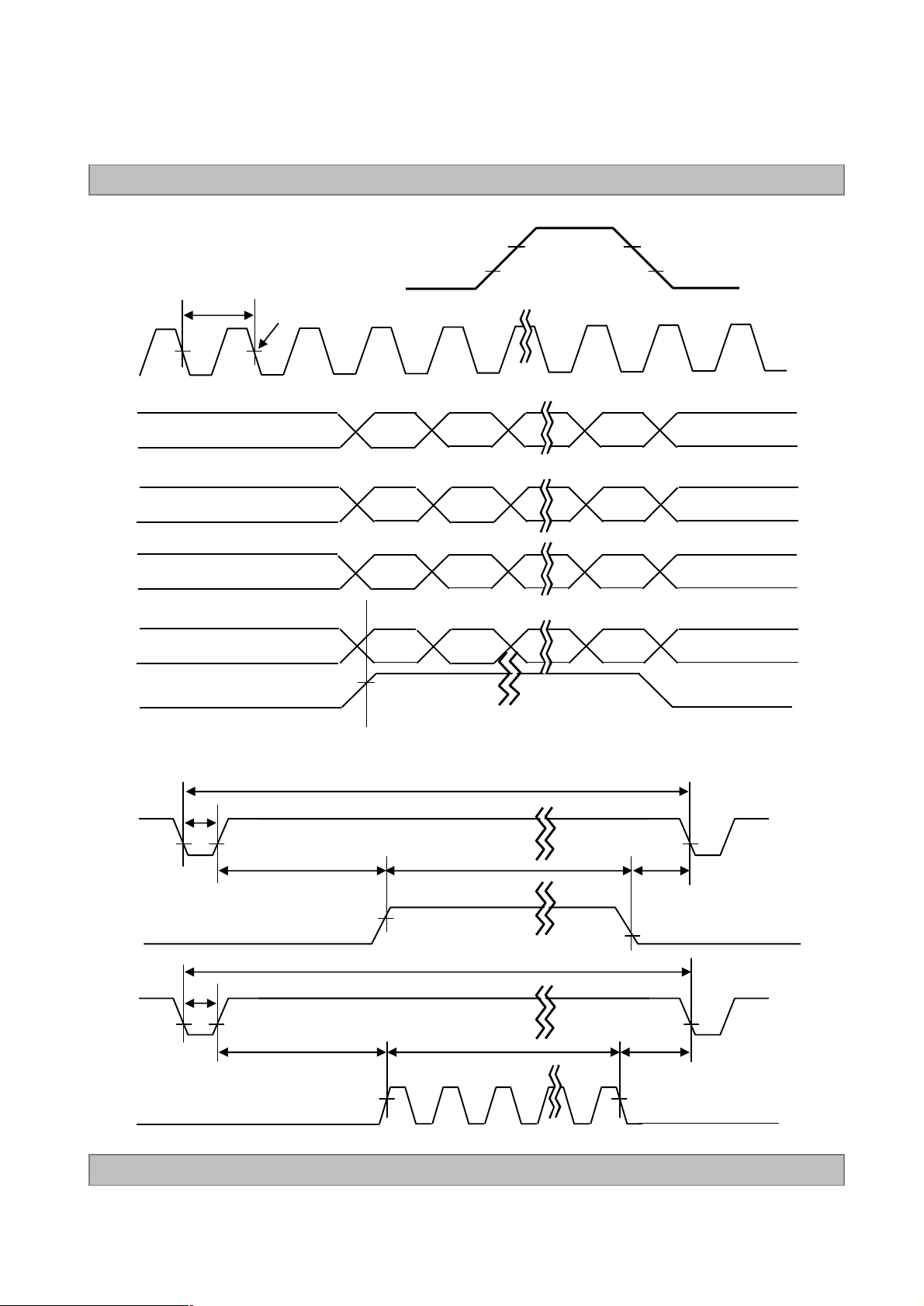
3-6. Power Sequence
3-6-1. LCD Driving circuit
LC470WUD
Product Specification
Power Supply For LCD
0V
0V
10%
Interface Signal (Tx)
V
LCD
Option Signal
(LVDS_select, DCR_Enable, BIT_select)
Power for Lamp
Table 9. POWER SEQUENCE
Parameter
90%
T1
T2
Invalid
Data
T7 T8
Valid Data
T3 T4
Lamp ON
Value
MaxTypMin
--200T4
-
-
T2
-
Invalid
Data
T5
Unit
ms20-0.5T1
ms--0T2
ms--200T3
ms
ms--0T5
s--2.0T6
ms0T7
ms0T8
90%
10%
T6
Notes
4
3
3
5
4
4
Note : 1. Please avoid floating state of interface signal at invalid period.
2. When the interface signal is invalid, be sure to pull down the power supply V
3. The T3/T4 is recommended value, the case when failed to meet a minimum specification,
abnormal display would be shown. There is no reliability problem.
4. If the on time of signals(Interface signal and Option signals) precedes the on time of Power(V
check the LCD logic Power(Vcc) is under 0.8V, otherwise it will be happened abnormal display.
5. T6 should be measured after the Module has beenfully discharged between power off and on
period.
Ver. 0.1
LCD
to 0V.
LCD
14/ 38
),
Page 15

3-6-2. Sequence for Inverter
Power Supply For Inverter
VBL
0V
10%
LC470WUD
Product Specification
24V (typ.)
90%
0.7V
T1 T2 T3 T2
VON/OFF
VBR-A &
VBR-B
3-6-3. Deep condition for Inverter
VBL(Typ.) x 0.8
Table 10. Power Sequence for Inverter
Parameter
1000ms (Min) 1000ms (Min)
T4
T5
T4
Lamp ON
T7
T6
V
: 24V
BL
0 V
Values
MaxTypMin
-
Units
ms--20T1
ms--500T2
ms--200T3
ms--10T5
VBL(Typ) x 0.8ms10--T6
Remarks
1
2ms0T4
3ms--1000T7
Notes : 1. T1 describes rising time of 0V to 24V and this parameter does not applied at restarting time.
2. T4(max) is less than T2.
3. In T7 section, VBR-B is recommended 3.3V.
Ver. 0.1
15/ 38
Page 16

LC470WUD
Product Specification
4. Optical Specification
Optical characteristics are determined after the unit has been ‘ON’ and stable in a dark environment at 25±2°C.
The values specified are at an approximate distance 50cm from the LCD surface at a viewing angle of Φ and θ
equal to 0 °.
FIG. 1 shows additional information concerning the measurement equipment and method.
Optical Stage(x,y)
LCD Module
FIG. 1 Optical Characteristic Measurement Equipment and Method
Table 11. OPTICAL CHARACTERISTICS
SymbolParameter
Contrast Ratio
Surface Luminance, white
Luminance Variation
Response Time
Color Coordinates
[CIE1931]
MPRT ms108G to G
RED
GREEN
BLUE
WHITE
WH
WHITE
-
-
Rx
Wx
Wy
5P
50cm
Typ
-0.03
Pritchard 880 or
equivalent
Ta= 25±2°C, V
, VBR-A=1.65V, VBR-B=3.3V
=12.0V, fV=120Hz, Dclk=297MHz
LCD
Value
MaxTypMin
-1100800CR
500400L
85-
0.647
0.329Ry
0.218Gx
0.666Gy
0.148Bx
0.067By
0.279
0.292
Typ
+0.03
ms
NoteUnit
1
2
2cd/m
31.3δ
4,5
Viewing Angle (CR>10)
x axis, right(φ=0°)
x axis, left (φ=180°)
y axis, up (φ=90°)
y axis, down (φ=270°)
Ver. 0.1
--89θr
--89θl
--89θu
--89θd
6degree
7Gray Scale 2.2
16/ 38
Page 17

Product Specification
Notes :1. Contrast Ratio(CR) is defined mathematically as :
CR(Contrast Ratio) = Maximum CRn (n=1, 2, 3, 4,5)
Surface Luminance at position n with all white pixels
CRn =
Surface Luminance at position n with all black pixels
n = the Position number(1, 2, 3, 4, 5). For more information, see FIG 2.
※ DCR Application : Refer to Appendix-V
2. Surface luminance are determined after the unit has been ‘ON’ and 30min afterlighting the
backlight in a dark environmentat 25±2°C. Surface luminance is the luminance value at center
1-point across the LCD surface 50cm from the surface with all pixels displaying white.
For more information see the FIG. 2.
3. The variation in surface luminance , δ WHITE is defined as :
δ WHITE(5P) = Maximum(L
Where L
on1
to L
are the luminance with all pixels displaying white at 5 locations.
on5
on1,Lon2
For more information, see the FIG. 2.
4. Response time is the time required for the display to transition from G(N) to G(M) (Rise Time, TrR)
and from G(M) to G(N) (Decay Time, TrD). For additional information see the FIG. 3. (N<M)
※ G to G Spec is average of measured time (N, M = 0 (Black) ~ 1023(White), 128 gray step).
5. MPRT is defined as the 10% to 90% blur-edge width Bij(pixels) and scroll speed U(pixels/frame)at
the moving picture. For more information, see FIG 4
6. Viewing angle is the angle at which the contrast ratio is greater than 10. The angles are
determined for the horizontal or x axis and the vertical or y axis with respect to the z axis which
is normal to the LCD module surface. For more information, seethe FIG. 5.
7. Gray scale specification
Gamma Value is approximately 2.2. For more information, see the Table 12.
, L
on3
, L
on4
, L
) / Minimum(L
on5
on1,Lon2
, L
on3
, L
on4
, L
LC470WUD
)
on5
Table 12. GRAY SCALE SPECIFICATION
Gray Level
L0
L63
L127
L191
L255
L319
L383
L447
L511
L575
L639
L703
L767
L831
L895
L959
L1023
Ver. 0.1
Luminance [%] (Typ.)
0.08
0.22
1.03
2.52
4.74
7.74
11.56
16.22
21.76
28.20
35.56
43.85
53.10
63.33
74.54
86.76
100
17/ 38
Page 18

Product Specification
Measuring point for surface luminance & measuring point for luminance variation
H
A
③②
LC470WUD
V
①
B
④
FIG. 2 5 Points for Luminance Measure
Response time is defined as the following figure and shall be measured by switching the input signal for
“Gray(N)” and “Gray(M)”.
TrR
100
90
Optical
Response
⑤
TrD
A : H / 4 mm
B : V / 4 mm
@ H,V : Active Area
Ver. 0.1
10
0
Gray(N)
N,M = Black ~ White, N<M
FIG.3 Response Time
Gray(M)
Gray(N)
18/ 38
Page 19

LC470WUD
Product Specification
MPRT is defined as the 10% to 90% blur-edge with Bij(pixels) and scroll speed U(pixels/frame)at the moving
picture.
1
M =
Bij (i=j)
U
Example) Bij = 12pixels, U = 10pixels / 120Hz
M = 12pixels / (10pixels / 120Hz)
= 12pixels / {10pixels / (1/120)s}
= 12 / 1,200 s
= 10 ms
Dimension of viewing angle range
φ
= 180°, Left
Lj
Li
FIG. 4 MPRT
Normal
θ
E
Y
Bij
φ
= 90°, Up
90%
10%
Ver. 0.1
φ
= 270°, Down
φ
FIG. 5 Viewing angle
φ
= 0°, Right
19/ 38
Page 20

Product Specification
5. Mechanical Characteristics
Table 13 provides general mechanical characteristics.
Table 13. MECHANICAL CHARACTERISTICS
LC470WUD
ValueItem
1096.0 mmHorizontal
Outline Dimension
Bezel Area
Active Display Area
14.5 Kg (Typ.), 15.5kg (Max.)Weight
Note : Please refer to a mechanic drawing in terms of tolerance at the next page.
640.0 mmVertical
53.1 mmDepth
1049.0 mmHorizontal
593.0 mmVertical
1039.68 mmHorizontal
584.82 mmVertical
Ver. 0.1
20/ 38
Page 21

<FRONT VIEW>
LC470WUD
Product Specification
Ver. 0.1
21/ 38
Page 22

<REAR VIEW>
LC470WUD
Product Specification
Ver. 0.1
22/ 38
Page 23

Product Specification
6. Reliability
Table 14. ENVIRONMENT TEST CONDITION
Vibration test
5
(non-operating)
Shock test
6
(non-operating)
LC470WUD
ConditionTest ItemNo.
Ta= 60°C 240hHigh temperature storage test1
Ta= -20°C 240hLow temperature storage test2
Ta= 50°C 50%RH 240hHigh temperature operation test3
Ta= 0°C 240hLow temperature operation test4
Wave form : random
Vibration level : 1.0G RMS
Bandwidth : 10-300Hz
Duration : X,Y,Z, 30 min
One time each direction
Shock level :50G(X,Y axis) , 35G(Z axis)
Waveform : half sine wave, 11ms
Direction : ±X, ±Y, ±Z
One time each direction
Ta= 40 °C, 90%RH, 240hHumidity condition Operation7
Altitude operating
8
storage / shipment
0 -14,000 feet(4267.2m)
0 -40,000 feet(12192m)
Note : Before and after Reliability test, LCM should be operated with normal function.
Ver. 0.1
23/ 38
Page 24

Product Specification
7. International Standards
7-1. Safety
a) UL 60065, 7thEdition, dated June 30, 2003, Underwriters Laboratories, Inc.,
Standard for Audio, Video and Similar Electronic Apparatus.
b) CAN/CSA C22.2, No. 60065:03, Canadian Standards Association,
Standard for Audio, Video and Similar Electronic Apparatus.
c) IEC60065:2001, 7thEdition CB-scheme and EN 60065:2002,
Safety requirements for Audio, Video and Similar Electronic Apparatus..
7-2. EMC
a) ANSI C63.4 “Methods of Measurement of Radio-Noise Emissions from Low-Voltage Electrical and
Electrical Equipment in the Range of 9kHZ to 40GHz. “American National Standards Institute(ANSI),
1992
b) CISPR13 "Limits and Methods of Measurement of Radio interference characteristics of Sound
and Television broadcast receivers and associated equipment"
CISPR22 "Limits and Methods of Measurement of Radio interference characteristics of Information
Technology Equipment" International Special Committeeon Radio Interference.
c) EN55013 "Limits and Methods of Measurement of Radio interference characteristics of Sound and
Television broadcast receivers and associated equipment"
EN55022 "Limits and Methods of Measurement of Radio interference characteristics of Information
Technology Equipment" European Committee for Electro Technical Standardization.(CENELEC),
1988(Including A1:2000)
LC470WUD
Ver. 0.1
24/ 38
Page 25

Product Specification
8. Packing
8-1. Designation of Lot Mark
a) Lot Mark
ABCDEFGHIJKLM
A,B,C : SIZE(INCH)
D : YEAR E : MONTH
F : PANEL CODEG : FACTORY CODE
H : ASSEMBLY CODE I,J,K,L,M : SERIAL NO.
Note
1. YEAR
Year
200320022001
200452005
2006720078200892009
LC470WUD
2010
Mark
321
4
6
2. MONTH
Month
Mark
Apr5May
4
Jun7Jul8Aug9Sep
6
b) Location of Lot Mark
Serial NO. is printed on the label. The label is attached to thebackside of the LCD module.
This is subject to change without prior notice.
8-2. Packing Form
a) Package quantity in one pallet : 12 pcs
b) Pallet Size : 1300mm X 1140mm X 860mm
0
Oct
A
Nov
B
DecMarFebJan
C421
Ver. 0.1
25/ 38
Page 26

LC470WUD
Product Specification
9. Precautions
Please pay attention to the followings when you use this TFT LCDmodule.
9-1. Mounting Precautions
(1) You must mount a module using holes arranged in four cornersor four sides.
(2) You should consider the mounting structure so that uneven force (ex. Twisted stress) is not applied to the
module. And the case on which a module is mounted should have sufficient strength so that external
force is not transmitted directly to the module.
(3) Please attach the surface transparent protective plate to the surface in order to protect the polarizer.
Transparent protective plate should have sufficient strength in order to the resist external force.
(4) You should adopt radiation structure to satisfy the temperature specification.
(5) Acetic acid type and chlorine type materials for the cover case are not desirable because the former
generates corrosive gas of attacking the polarizer at high temperature and the latter causes circuit break
by electro-chemical reaction.
(6) Do not touch, push or rub the exposed polarizers with glass,tweezers or anything harder than HB
pencil lead. And please do not rub with dust clothes with chemical treatment.
Do not touch the surface of polarizer for bare hand or greasy cloth.(Some cosmetics are detrimental
to the polarizer.)
(7) When the surface becomes dusty, please wipe gently with absorbent cotton or other soft materials like
chamois soaks with petroleum benzine. Normal-hexane is recommended for cleaning the adhesives
used to attach front / rear polarizers. Do not use acetone, toluene and alcohol because they cause
chemical damage to the polarizer.
(8) Wipe off saliva or water drops as soon as possible. Their long time contact with polarizer causes
deformations and color fading.
(9) Do not open the case because inside circuits do not have sufficient strength.
9-2. Operating Precautions
(1) The spike noise causes the mis-operation of circuits. It should be lower than following voltage:
V=±200mV(Over and under shoot voltage)
(2) Response time depends on the temperature.(In lower temperature, it becomes longer.)
(3) Brightness depends on the temperature. (In lower temperature, it becomes lower.)
And in lower temperature, response time(required time that brightness is stable after turned on)
becomes longer
(4) Be careful for condensation at sudden temperature change.Condensation makes damage to polarizer or
electrical contacted parts. And after fading condensation, smear or spot will occur.
(5) When fixed patterns are displayed for a long time, remnantimage is likely to occur.
(6) Module has high frequency circuits. Sufficient suppressionto the electromagnetic interference shall be
done by system manufacturers. Grounding and shielding methods may be important to minimized the
interference.
(7) Please do not give any mechanical and/or acoustical impactto LCM. Otherwise, LCM can’t be operated
its full characteristics perfectly.
(8) A screw which is fastened up the steels should be a machine screw.
(if not, it can causes conductive particles and deal LCMa fatal blow)
(9)Please do not set LCD on its edge.
(10) It is recommended to avoid the signal cable and conductive material over the inverter transformer
for it can cause the abnormal display and temperature rising.
(11) Partial darkness may happen during 3~5 minutes when LCM is operated initially in condition that
luminance is under 40% at low temperature (under 5℃). This phenomenon which disappears naturally
after 3~5 minutes is not a problem about reliability but LCD characteristic
Ver. 0.1
26/ 38
Page 27

LC470WUD
Product Specification
9-3. Electrostatic Discharge Control
Since a module is composed of electronic circuits, it is not strong to electrostatic discharge. Make certain that
treatment persons are connected to ground through wrist band etc. And don’t touch interface pin directly.
9-4. Precautions for Strong Light Exposure
Strong light exposure causes degradation of polarizer and color filter.
9-5. Storage
When storing modules as spares for a long time, the following precautions are necessary.
(1) Store them in a dark place. Do not expose the module to sunlight or fluorescent light. Keep the temperature
between 5°C and 35°C at normal humidity.
(2) The polarizer surface should not come in contact with any other object.
It is recommended that they be stored in the container in which they were shipped.
9-6. Handling Precautions for Protection Film
(1) The protection film is attached to the bezel with a small masking tape.
When the protection film is peeled off, static electricity is generated between the film and polarizer.
This should be peeled off slowly and carefully by people who are electrically grounded and with well ionblown equipment or in such a condition, etc.
(2) When the module with protection film attached is stored for a long time, sometimes there remains a very
small amount of glue still on the bezel after the protection film is peeled off.
(3) You can remove the glue easily. When the glue remains on thebezel surface or its vestige is recognized,
please wipe them off with absorbent cotton waste or other soft material like chamois soaked with normalhexane.
Ver. 0.1
27/ 38
Page 28
Product Specification
# APPENDIX-I-1
■ REQUIRED SIGNAL ASSIGNMENT FOR LVDS TRANSMITTER ( Pin7=“L ”)
LC470WUD
Host System
24 Bit
R10/R20
R11/R21
R12/R22
R13/R23
R14/R24
R15/R25
R16/R26
R17/R27
G10/G20
G11/G21
G12/G22
G13/G23
G14/G24
G15/G25
G16/G26
G17/G27
B10/B20
B11/B21
B12/B22
B13/B23
B14/B24
B15/B25
B16/B26
B17/B27
Hsync
Vsync
Data Enable
CLOCK
THC63LVD823
or Compatible
53/81
54/82
57/83
58/84
59/85
60/86
51/79
52/80
63/91
64/92
65/93
66/94
67/95
68/96
61/89
62/90
73/99
74/100
75/1
76/2
77/5
78/6
69/97
70/98
7
8
9
10
TA1-TA1+
TB1-/TB1+
TC1-/TC1+
TCLK1-
TCLK1+
TD1-/TD1+
TA2-/TA2+
TB2-/TB2+
TC2-/TC2+
TCLK2-
TCLK2+
TD2-/TD2+
49
48
47
46
44
43
42
41
40
39
37
36
35
34
32
31
30
29
28
27
Ground
FI-R51S-HF
12
13
14
15
16
17
19
20
22
23
28
29
30
31
32
33
35
36
38
39
7
10
100Ω
100Ω
100Ω
100Ω
100Ω
100Ω
100Ω
100Ω
100Ω
100Ω
LCD Module
Timing
Controller
RA1N
RA1P
RB1N
RB1P
RC1N
RC1P
RCLK1N
RCLK1P
RD1N
RD1P
RA2N
RA2P
RB2N
RB2P
RC2N
RC2P
RCLK2N
RCLK2P
RD2N
RD2P
VESA / JEIDA
DCR Enable
Notes :1. The LCD module uses a 100 Ohm[Ω] resistor between positive and negative lines of each receiver
input.
2. Refer to LVDS Transmitter Data Sheet for detail descriptions. (THC63LVD103 or Compatible)
3. ‘9’ means MSB and ‘0’ means LSB at R,G,B pixel data.
Ver. 0.1
28/ 38
Page 29

Product Specification
# APPENDIX-I-2
■ REQUIRED SIGNAL ASSIGNMENT FOR LVDS TRANSMITTER ( Pin7=“H” )
LC470WUD
Host System
24 Bit
R10/R20
R11/R21
R12/R22
R13/R23
R14/R24
R15/R25
R16/R26
R17/R27
G10/G20
G11/G21
G12/G22
G13/G23
G14/G24
G15/G25
G16/G26
G17/G27
B10/B20
B11/B21
B12/B22
B13/B23
B14/B24
B15/B25
B16/B26
B17/B27
Hsync
Vsync
Data Enable
CLOCK
THC63LVD823
or Compatible
51/79
52/80
53/81
54/82
57/83
58/84
59/85
60/86
61/89
62/90
63/91
64/92
65/93
66/94
67/95
68/96
69/97
70/98
73/99
74/100
75/1
76/2
77/5
78/6
7
8
9
10
TA1-TA1+
TB1-/TB1+
TC1-/TC1+
TCLK1-
TCLK1+
TD1-/TD1+
TA2-/TA2+
TB2-/TB2+
TC2-/TC2+
TCLK2-
TCLK2+
TD2-/TD2+
49
48
47
46
44
43
42
41
40
39
37
36
35
34
32
31
30
29
28
27
VCC
FI-R51S-HF
12
13
14
15
16
17
19
20
22
23
28
29
30
31
32
33
35
36
38
39
7
10
100Ω
100Ω
100Ω
100Ω
100Ω
100Ω
100Ω
100Ω
100Ω
100Ω
LCD Module
Timing
Controller
RA1N
RA1P
RB1N
RB1P
RC1N
RC1P
RCLK1N
RCLK1P
RD1N
RD1P
RA2N
RA2P
RB2N
RB2P
RC2N
RC2P
RCLK2N
RCLK2P
RD2N
RD2P
VESA/JEIDA
DCR Enable
Notes :1. The LCD module uses a 100 Ohm[Ω] resistor between positive and negative lines of each receiver
input.
2. Refer to LVDS Transmitter Data Sheet for detail descriptions. (THC63LVD103 or Compatible)
3. ‘9’ means MSB and ‘0’ means LSB at R,G,B pixel data.
Ver. 0.1
29/ 38
Page 30

# APPENDIX-II
■ Pallet Ass’y
LC470WUD
Product Specification
Ver. 0.1
MATERIALDESCRIPTIONNO.
LCD Module1
47INCHBAG2
MASKING 20MMX50MTAPE3
PAPER 1300X1140X130MMPALLET4
EPSPACKING,BOTTOM5
EPSPACKING,TOP6
PAPER ANGLE,POST7
PAPERANGLE,PACKING8
STEELBAND,CLIP9
PPBAND10
OPPTAPE11
YUPO 80G 100X100LABEL12
30/ 38
Page 31

LC470WUD
# APPENDIX 2
# APPENDIX-III
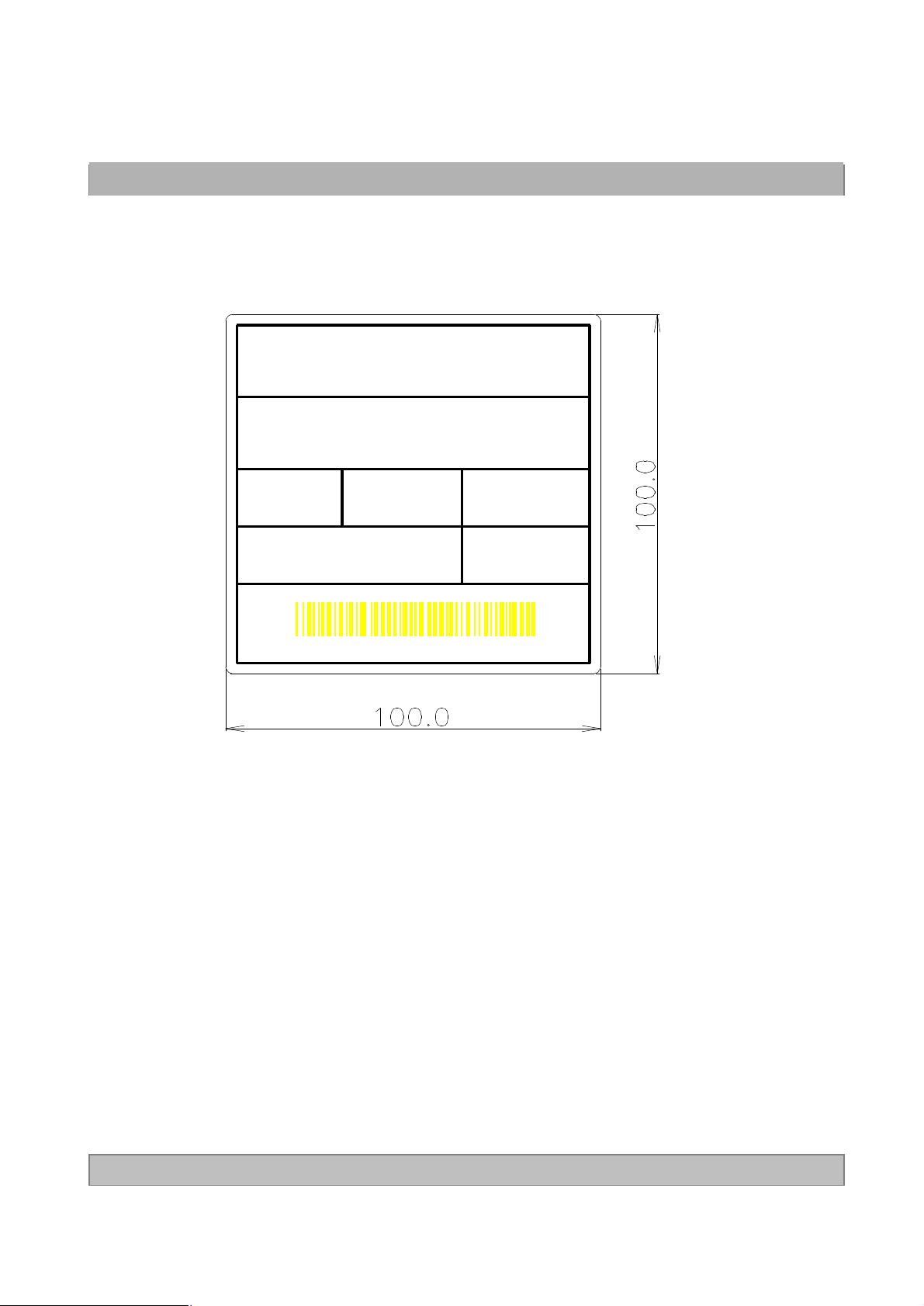
■ LCM Label
Model
UL, TUV Mark
LPL Logo
US PATENT No.
Product Specification
LC470WUD
(SA)(B1)
Serial No.
Origin
Ver. 0.1
31/ 38
Page 32
LC470WUD
# APPENDIX 3
# APPENDIX-IV
■ Pallet Label
Product Specification
LC470WUD
SAB1
12 PCS
MADE IN KOREA RoHS Verified
001/01-01
XXXXX XXXXXXXX XXX XXX XXXX
Ver. 0.1
32/ 38
Page 33

# APPENDIX-V-1
LC470WUD
Product Specification
■ LCM DCR Only (Reference)
NTSC / PAL
Sync_PWM
FFC Cable
System
LCM
Master
Inverter
14
1
Board
13
11
VBR-B
3.3V
VBR-A
NC / 1.65V
LCM Control Board
Pin : VBR_EXT
Pin : VBR_OUT
#10
DCR_Enable Pin
VBR-B
511
3.3V
12V
LCM
Slave
Inverter
1
12
■ DCR_EnableOption Pin Description
VBR_OUT
(VBR-B)
From T-Con
(ASIC)
Signal Source
Ver. 0.1
Off (0V)On(3.3V)DCR_Enable
From System
(VBR_EXT Pin)
3.3V0V ~ 3.3VVBR-B
1.65V or NC1.65V or NCVBR-A
1300 : 12600 : 1DCR Level
Gray Level
L0
L63
L127
L191
L255
L319
L383
L447
L511
L575
L639
L703
L767
L831
L895
L959
L1023
Luminance [%] DCR On
VBR-A = 1.65V
0.05
0.24
0.82
1.90
3.64
6.37
9.8
13.9
18.5
24.0
31.1
38.1
46.7
56.9
69.5
83.8
100
33/ 38
Page 34

Product Specification
# APPENDIX-V-2
■ System DCR (Dynamic Contrast Ratio)-Max 13000:1 (Reference)
LC470WUD
LCM
Master
Inverter
14
FFC Cable
1
NTSC / PAL
Sync_PWM
System
Board
13
11
LCM Control Board
511
511
12V
#10 : DCR Enable Pin
VBR-B
0V ~ 3.3V
VBR-A
0V ~ 1.65V
3.3V0V ~ 3.3VVBR-B
1.65V0V ~ 1.65VVBR-A
VBR-A : 1.65V
VBR-B : 3.3V
Maximum Brightness (100%)
(DCR Condition)
LCM
Slave
Inverter
1
12
FunctionVBR-A,B Voltage
1300 : 113000 : 1DCR Level
Minimum Brightness (10%)0V
Note : 1. To make DCR Max 13000:1, VBR-A and VBR-B must be given by system.
2. DCR Max 13000:1 is defined mathematically as :
DCR = Maximum DCRn (n=1, 2, 3, 4, 5)
DCRn =
Surface Luminance at position n with all white pixels (VBR-B=3.3V, VBR-A=1.65V)
Surface Luminance at position n with all black pixels (VBR-B=0V, VBR-A=0V)
n = the Position number(1, 2, 3, 4, 5). For more information, see FIG 2.
3. Measurement Sequence (aging time 10 min each pattern) :
① Turn On LCM
② Measure Black Luminance (VBR-B=0V, VBR-A=0V)
③ Measure White Luminance (VBR-B=3.3V, VBR-A=3.3V)
4. In case the lowest minimum brightness is continued,
it can affect the lamp reliability and appear the partial darkness.
Ver. 0.1
34/ 38
Page 35

Product Specification
# APPENDIX-VI
Option Pin Circuit Block Diagram
Circuit Block Diagram of LVDS Format Selection pin
LC470WUD
240Ω
Selector (Pin 7) Selector
50KΩ
ASIC
(TCON)
System SideLCM Side
Ver. 0.1
35/ 38
Page 36

# APPENDIX-VII
1. DC Specification
LVDS -
LVDS +
LVDS Input characteristics
# |VID| = |(LVDS+) ?(LVDS-)|
# VCM= {(LVDS+) + (LVDS-)}/2
0V
Product Specification
|VID|
LC470WUD
V
CM
NotesUnitMaxMinSymbolDescription
LVDS Common mode Voltage
2. AC Specification
1 ) LVDS Clock to data timing
LVDS Clock
LVDS Data
LVDS Clock to Data Skew Margin
-mV600200|VID|LVDS Differential Voltage
CM
Tc
SKEW (Fclk
t
SKEW
t
= 1/T
clk
)
-V1.51.0V
NotesUnitMaxMinSymbolDescription
SKEW
Note 1ps+(Tc/ 7)* 0.2-(Tc/ 7)* 0.2t
Ver. 0.1
36/ 38
Page 37

2 ) LVDS Clock timing
LVDS 1’st Clock
LVDS 2nd/ 3rd/ 4thClock
LVDS inter-port Clock Skew
T
skew_minTskew_max
< LVDS inter-port Clock timing >
Product Specification
T
clk
skew
LC470WUD
NotesUnitMaxMinSymbolDescription
-ns2.5-2.5T
Ver. 0.1
37/ 38
Page 38

# APPENDIX-VIII
■ LVDS Select : “H” Data-Mapping (JEIDA format)
RCLKP
RCLKM
LC470WUD
Product Specification
LVDS Data-Mapping info. (10bit)
RAP
RBP
RCP
RDP
REP
R19 R18 R17 R16G14 R15R14’ R14R15’ G14”
B14 G19 G18 G17B15 G16G15’ G15G16’ B15”
V
SYNCHSYNC
B13 B12 G13 G12X R13R12’ R12R13’ X”
B11 B10 G11 G10X R11R10’ R10R11’ X”
B19 B18DE B17B16’ B16B17’ DE”
■ LVDS Select : “L” Data-Mapping (VESA format)
RCLKP
RCLKM
RAP
RBP
R15 R14 R13 R12G10 R11R10’ R10R11’ G10”
B10 G15 G14 G13B11 G12G11’ G11G12’ B15”
Ver. 0.1
RCP
RDP
REP
V
SYNCHSYNC
B17 B16 G17 G16X R17R16’ R16R17’ X”
B19 B18 G19 G18X R19R18’ R18R19’ X”
B15 B14DE B13B12’ B12B13’ DE”
38/ 38
 Loading...