

Page 1
LC4
LC4
2
0W
2
0W
X7--
X7
(120Hz HD)
(120Hz HD)
SLE1 Promotion
SLE1 Promotion
Apr.16th, 2007
Confidential
0/14
Page 2
LC422
LC4
Specification
Specification
0W
0W
X7--
X7
SLE1 Promotion
SLE1 Promotion
• Resolution : WXGA(1366x768)
• Dimension: 983X576X51mm
• Luminance : 500nits
• Response time : 10ms(MPRT)
• Contrast Ratio : 1000:1
• Viewing angle : 178/178
Development Schedule
Development Schedule
[
Base on the ETD
[
Base on the ETD
LPL
Development
Schedule
]
]
07
‘‘07
C,M,P Test
4/E
• Interface : LVDS 2Port
• Color Temperature : 10,000K
• Color Depth : 8bit (16.7M) / 10bit (1B)
• Color Gamut : 72%
• ETC : Zero RT POL
RV
5/E
PV
6/M
MP
6/E
Buyer
Development
Schedule
Confidential
07
‘‘07
1/14
ES
6/12
2ea
PP
7/20
30ea
MP
Page 3
LC422
LC4
¾
¾
0W
X7--
0W
X7
Master
Master
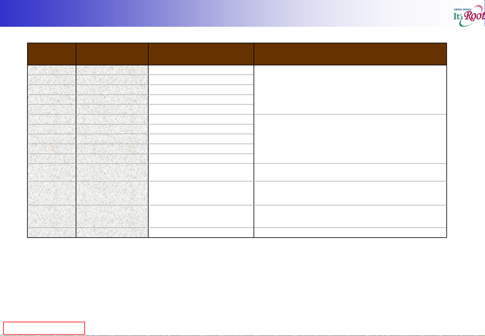
Customer Specification LC420WX4-SLB1 [ MP Model ] LC420WX7-SLE1 [ NEW Model ] Note
SLE1 Promotion
SLE1 Promotion
Outline Dimension 983 x 576 x 51mm(with inverter)
Brightness[nit] 500nit
R/T(MPRT) [ms] 10 ms
Color Gamut [%] 72%
Viewing Angle [ ˚] 178/178
Contrast Ratio Typ. 1000:1
User Interface LVDS 2Port
Color Depth 8Bit / 10 Bit
Color Temp. 10,000K
# of Lamps H-H (CCFL)
Input Voltage 12V/24V
Power Consumption Logic:8.2W / Inverter:171W
Polarizer ZRT
Input Connector 51 pin
Å
Å
Å
Å
Å
Å
Å
Å
Å
H-H (EEFL)
12V/24V
Logic:8.2W (Not Fixed) / Inverter:162W (Not Fi
xed)
Å
Å
Inverter Pin
Mounting Type Rear Mount
Weight Typ. 13.0Kg
MP Plan MP
Confidential
M : 14Pin
S : 12Pin
Å
Rear Mount / Front Mount
Typ. 10.5Kg (Not Fixed)
07’,6/B
2/14
Page 4
APPENDIX I. LVDS 51 Pin Configuration
APPENDIX I. LVDS 51 Pin Configuration
- LCD Connector(CN1) : FI-R51S-HF (Manufactured by JAE) or Equivalent
- Mating Connector : FI-R51HL (Manufactured by JAE) or Equivalent
No Symbol Description No Symbol Description
1
2
3
4 NC
5
6
7 LVDS Select LVDS Format / Refer to Note 1
8
9
10 DCR Enable DCR Selection / Refer to Note 2
11
12
13
14
15 RO1P FIRST CHANNEL 1+
16
17
18
19
20 ROCLKP FIRST CLOCK CHANNEL C+
21
22
23
24
25
26 GND Ground
GND
NC
NC
NC
NC
VBR_EXT
VBR_OUT VBR output form LCD module
GND
RO0N
RO0P
RO1N
RO2N
RO2P
GND
ROCLKN
GND
RO3N
RO3P
RO4N
RO4P
Ground
No Connection
No Connection
No Connection
No Connection
No Connection
External VBR input from System
Ground
FIRST CHANNEL 0FIRST CHANNEL 0+
FIRST CHANNEL 1-
FIRST CHANNEL 2FIRST CHANNEL 2+
Ground
FIRST CLOCK CHANNEL C-
Ground
FIRST CHANNEL 3FIRST CHANNEL 3+
FIRST CHANNEL 4FIRST CHANNEL 4+
27
28
29
30
31
32
33
34
35
36
37
38
39
38
39
42
43
44
45
46
47
48
49
50
51
BIT Select
RE0N
RE0P
RE1N
RE1P
RE2N
RE2P
GND
RECLKN
RECLKP
GND
RE3N
RE3P
RE4N
RE4P
GND
GND
GND
GND
GND
NC
VLCD
VLCD
VLCD
VLCD
-
Logic ‘L’ : 8bit, ‘H’ or ‘NC’ : 10bit
SECOND CHANNEL 0SECOND CHANNEL 0+
SECOND CHANNEL 1SECOND CHANNEL 1+
SECOND CHANNEL 2SECOND CHANNEL 2+
Ground
SECOND CLOCK CHANNEL CSECOND CLOCK CHANNEL C+
Ground
SECOND CHANNEL 3SECOND CHANNEL 3+
SECOND CHANNEL 4SECOND CHANNEL 4+
Ground
Ground
Ground (NSB) / / Refer to Note 3
Ground
Ground
No connection
Power Supply +12.0V
Power Supply +12.0V
Power Supply +12.0V
Power Supply +12.0V
--
Confidential
3/14
Page 5
APPENDIX II. Inverter Pin Configuration
APPENDIX II. Inverter Pin Configuration
Inverter Pin Configuration( Equivalent to LC420WX4-SLB1 MP Model )
Pin No Symbol Description Note
1
2
3
4
5
6
7
8
9
10
11
12
13
14
VBL 24V Input
VBL
VBL
VBL
VBL
GND
GND
GND
GND
GND
VBR-A
V On/Off
VBR-B
NC NC
Backlight ON/OFF control
24V Input
24V Input
24V Input
24V Input
Analog dimming
0.0V ~ 3.3V (DC)
GND
GND
GND
GND
GND
0V(min) ~ 3.3V(max)
Open : VBR-A=1.65V
ON : 2.5 ~ 5.0V
OFF : -0.3 ~ 0.8V
0V(min) ~ 3.3V(max)
Open : Duty=100%,
if you don’t use DCR function, please appl y 3.3Volt or let it “Open”.
NC
1. Master Connector
1) Connector(Receptacle)
: S14B-PH-SMC (manufactured JST) or Equivalent
2) Mating Connector (Plug)
: PHR14 (manufactured JST) or Equivalent
*JST: Japan S o ldeerless Terminal Co., LTD
Confidential
2. Slave Connector
1) Connector(Receptacle)
: S12B-PH-SMC (manufactured JST) or Equivalent
2) Mating Connector (Plug)
: PHR12 (manufactured JST) or Equivalent
4/14
Page 6

APPENDIX III. Mechanical Change [ Overall ]
APPENDIX III. Mechanical Change [ Overall ]
Overall
Front
Rear
LC420WX4-SLB1 LC420WX7-SLE1
Remarks
Confidential
1. Changed the user mount shape ( Front Mount Applied : 12ea)
2. Changed Inverter Size
3. Changed shape of Cover Shield(Control PCB)
5/14
Page 7

APPENDIX IV. Mechanical Change [ Front ]
APPENDIX IV. Mechanical Change [ Front ]
LC420WX7-SLE1Front LC420WX4-SLB1
Remarks
Confidential
Front User Mounting Hole : Nothing
1. User mount
6/14
Corner : 4 ea
Corner Left/Right Down
User Mounting Hole 6-M4
Left/Right : 4 ea
Down : 4 ea
Page 8

APPENDIX IV. Mechanical Change [ Rear ]
APPENDIX IV. Mechanical Change [ Rear ]
LC420WX7-SLE1 THM (Front Mount)Rear
100
100
486.5
344
180
486.5
344
180
100
100
Confidential
486.5
300
100
100
300
486.5
7/14
Page 9

APPENDIX IV. Mechanical Change [ Rear ]
APPENDIX IV. Mechanical Change [ Rear ]
Rear LC420WX7-SLE1LC420WX4-SLB1
Remarks
Confidential
1. Changed Inverter Size
8/14
Page 10

APPENDIX IV. Mechanical Change [ Rear ]
APPENDIX IV. Mechanical Change [ Rear ]
Rear LC420WX7-SLE1LC420WX4-SLB1
Remarks
Confidential
1. Changed corner shape. THM (Front Mount)
9/14
Page 11

APPENDIX IV. Mechanical Change [ Rear ]
APPENDIX IV. Mechanical Change [ Rear ]
Rear LC420WX7-SLE1LC420WX4-SLB1
Remarks
Confidential
1. Changed shape.
10/14
Page 12

APPENDIX IV. Mechanical Change [ Rear ]
APPENDIX IV. Mechanical Change [ Rear ]
Rear LC420WX7-SLE1LC420WX4-SLB1
Remarks
Confidential
1. Changed shape. THM (Front Mount)
11/14
Page 13

APPENDIX IV. Mechanical Change [ Side ]
APPENDIX IV. Mechanical Change [ Side ]
Top Side MountSide
LC420WX4-SLB1
Non-Side Mount
LC420WX7-SLE1
470 470
Side Mount 3ea
Confidential
12/14
Page 14

APPENDIX IV. Mechanical Change [ Side ]
APPENDIX IV. Mechanical Change [ Side ]
Bottom Side MountSide
LC420WX4-SLB1
Side Mount 4ea
LC420WX7-SLE1
335
115
220 220
220 220
115
115115
335
450 450
Side Mount 8ea
Confidential
13/14
Page 15

APPENDIX IV. Mechanical Change [ Side ]
APPENDIX IV. Mechanical Change [ Side ]
Side MountSide
LC420WX4-SLB1
Non-Side Mount
LC420WX7-SLE1
Side Mount 5ea
Confidential
220
140
140
220
14/14
 Loading...