

Page 1
LC420WX5
Liquid Crystal Display
Product Specification
SPECIFICATION
FOR
APPROVAL
)
(
(
Preliminary Specification
)
Final Specification
●
42.0” WXGA TFT LCDTitle
MODEL
APPROVED BY
/
/
/
PhilipsBUYER
SIGNATURE
DATE
LG.Philips LCD Co., Ltd.SUPPLIER
LC420WX5*MODEL
SLD1 (RoHS Verified)SUFFIX
*When you obtain standard approval,
please use the above model name without suffix
APPROVED BY
H. S Baek / G. Manager
REVIEWED BY
D. S Kim / Manager
PREPARED BY
Y. J Heo / Engineer
SIGNATURE
DATE
Please return 1 copy for your confirmation with
your signature and comments.
Ver. 1.0 Dec. 15, 2006
TV Products Development Dept.
LG. Philips LCD Co., Ltd
1 / 28
Page 2
Product Specification
CONTENTS
LC420WX5
Liquid Crystal Display
PageItemNumber
COVER
CONTENTS
RECORD OF REVISIONS
GENERAL DESCRIPTION1
ABSOLUTE MAXIMUM RATINGS2
ELECTRICAL SPECIFICATIONS3
ELECTRICAL CHARACTERISTICS3-1
INTERFACE CONNECTIONS3-2
SIGNAL TIMING SPECIFICATIONS3-3
SIGNAL TIMING WAVEFORMS3-4
COLOR INPUT DATA REFERENCE3-5
POWER SEQUENCE3-6
OPTICAL SPECIFICATIONS4
MECHANICAL CHARACTERISTICS5
RELIABILITY6
INTERNATIONAL STANDARDS7
1
2
3
4
5
6
6
8
12
13
14
15
17
21
24
25
SAFETY7-1
EMC7-2
PACKING8
DESIGNATION OF LOT MARK8-1
PACKING FORM8-2
PRECAUTIONS9
MOUNTING PRECAUTIONS9-1
OPERATING PRECAUTIONS9-2
ELECTROSTATIC DISCHARGE CONTROL9-3
PRECAUTIONS FOR STRONG LIGHT EXPOSURE9-4
STORAGE9-5
HANDLING PRECAUTIONS FOR PROTECTION FILM9-6
Ver. 1.0 Dec. 15, 2006
25
25
26
26
26
27
27
27
28
28
28
28
2 / 28
Page 3

Product Specification
RECORD OF REVISIONS
Preliminary Specification(First Draft) -Oct, 13. 20060.0
Change the Pallet Ass’y33Nov, 16. 2006
Update Mechanic drawing23
Update Electrical characteristics7Nov, 30. 20060.1
Update Optical characteristics17
Update Electrical characteristics7Dec, 15. 20061.0
Update the Appendix A and C
LC420WX5
Liquid Crystal Display
DescriptionPageRevision DateRevision No.
Ver. 1.0 Dec. 15, 2006
3 / 28
Page 4

LC420WX5
Liquid Crystal Display
Product Specification
1. General Description
The LC420WX5 is a Color Active Matrix Liquid Crystal Display with an integral Cold Cathode Fluorescent
Lamp(CCFL) backlight system. The matrix employs a-Si Thin Film Transistor as the active element.
It is a transmissive type display operating in the normally black mode. It has a 42.0 inch diagonally measured
act i ve dis p lay ar ea wi th WXG A re sol uti on (7 68 ve rti cal b y 1366 hor izo nta l pix el ar ray).
Each pixel is divided into Red, Green and Blue sub-pixels or dots which are arranged in vertical stripes.
Gray scale or the luminance of the sub-pixel color is determined with a 8-bit gray scale signal for each dot,
thus presenting a palette of more than 16.7M(true) colors.
It has been designed to apply the 8-bit 1-port LVDS interface.
It is intended to support LCD TV, PCTV where high brightness, super wide viewing angle, high color gamut,
high color depth and fast response time are important.
+12.0V
5pair
LVDS
Select
#9
+24.0V
GND
Status
CN1
(30pin)
General Features
SDRAM
MEM
CTRL
RGB
SCL
LVDS Rx (Receiver)
DCR Controller
TEMP ODC Controller
Timing Controller
Power Circuit
Block
Inverter
(CN2,CN3)
42.02 inches(1067.308mm) diagonalActive Screen Size
983 mm(H) x 576 mm(V) x 51 mm(D) (Typ.)Outline Dimension
0.227mm x 0.681mm x RGBPixel Pitch
1366 horiz. by 768 vert. Pixels RGB stripe arrangementPixel Format
8-bit, 16.7 M colorsColor Depth
500 cd/m2 (Center 1-point) (Typ.)Luminance, White
Viewing Angle Free ( R/L 178 (Typ.), U/D 178 (Typ))Viewing Angle (CR>10)
Total 164.76W (Typ.) (Logic=6.36 W, Inverter=162W [IBL=126mA] ) Power Consumption
11.5Kg (Typ.) Weight
Transmissive mode, Normally blackDisplay Operating Mode
EEPROM
(LUT)
Mini-LVDS(RGB)
SDA
Gate Driver Circuit
3Pin x 1CN (High)
3pin x 1CN (High)
Source Driver Circuit
S1 S1366
G1
TFT - LCD Panel
(1366 ×RGB ×768 pixels)
G768
Back light Assembly (18CCFL)
Hard coating(3H), Anti-glare treatment of the front polarizer (Haze 13%)Surface Treatment
Ver. 1.0 Dec. 15, 2006
4 / 28
Page 5
LC420WX5
Liquid Crystal Display
Product Specification
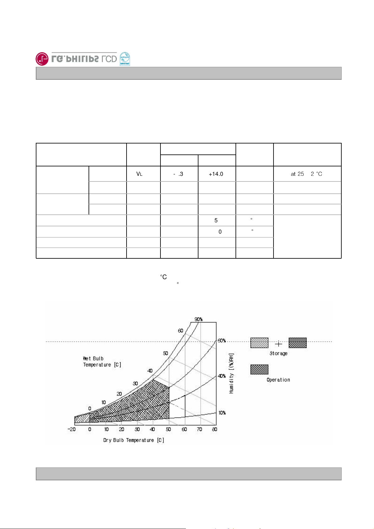
2. Absolute Maximum Ratings
The following items are maximum values which, if exceeded, may cause faulty operation or damage to the
LCD module.
Table 1. ABSOLUTE MAXIMUM RATINGS
Value
Parameter Remark
Symbol
Unit
MaxMin
Power Input
Voltage
Inverter Control
Voltage
LCD circuit
Inverter
ON/OFF
Brightness
Operating Temperature
Storage Temperature
Operating Ambient Humidity
Storage Humidity
LCD
BL
OFF/VON
BR_B
OP
ST
OP
ST
+14.0-0.3V
+28.021.6V
+5.25-0.3V
+5.00.0V
+500T
+50-20T
V
DC
V
DC
V
DC
V
DC
°
C
°
C
%RH9010H
%RH9010H
Note 1. Temperature and relative humidity range are shown in the figure below.
Wet bulb temperature should be 39 °C Max, and no condensation of water.
2. Gravity mura can be guaranteed under 40 °C condition.
at 25 ±2 °C
Note 1
Ver. 1.0 Dec. 15, 2006
5 / 28
Page 6
LC420WX5
Liquid Crystal Display
Product Specification
3. Electrical Specifications
3-1. Electrical Characteristics
It requires two power inputs. One is employed to power for the LCD circuit. The other input power for the
CCFL/Backlight is to power inverter.
Table 2. ELECTRICAL CHARACTERISTICS
Parameter Symbol
Value
Circuit :
Power Input Voltage
Power Input Current
Power Consumption
Rush current
LCD
I
LCD
LCD
RUSH
Note : 1. The specified current and power consumption are under the V
condition whereas mosaic pattern(8 x 6) is displayed and fVis the frame frequency.
2. The current is specified at the maximum current pattern.
3. The duration of rush current is about 2ms and rising time of power input is 1ms (min.).
White : 255Gray
Black : 0Gray
MaxTypMin
V
12.612.011.4V
=12.0V, 25 ± 2°C, fV=60Hz
LCD
DC
NoteUnit
1mA689530-
2mA780600-
1Watt8.276.36P
3A3.0--I
Mosaic Pattern(8 x 6)
Ver. 1.0 Dec. 15, 2006
6 / 28
Page 7
LC420WX5
Liquid Crystal Display
Product Specification
Table 3. ELECTRICAL CHARACTERISTICS (Continue)
Parameter Symbol
Inverter :
Power Supply
Input Current
Input Voltage for
Control System
Signals
After Aging
Before Aging
On/Off
Pulse Duty(PWM)
(Burst mode)
Audible Noise
Lamp :
Lamp Current (ExtVbr-B = 100%)
On Vdc5.0-2.5V on
Off
IBL_A
IBL_B
I
O-MAX
I
O-TYP
I
O-MIN
2.5 V
0.0
TsDischarge Stabilization Time
Notes :
1. Electrical characteristics are determined after the unit has been ‘ON’ and stable for approximately 120
minutes at 25±2°C. The specified current and power consumption are under the typical supply Input voltage
24V and Vbr 1.65V, it is total power consumption.
The ripple voltage of the power supply input voltage is under 0.4 Vp-p. LPL recommend Input Voltage is
24.0V ±5%.
2. Electrical characteristics are determined within 30 minutes at 25±2°C.
The specified currents are under the typical supply Input voltage 24V.
3.
Brightness Control. This VBRVoltage control brightness.
Boost Voltage
4.
LPL recommend that the PWM freq. is
Function
synchronized with the treble harmonic of Vsync signal of system.
5. The brightness of the lamp after lighted for 5minutes is defined as 100%.
TSis the time required for the brightness of the center of the lamp to be not less than 95% at typical current.
The screen of LCD module may be partially dark by the time the brightness of lamp is stable after turn on.
6. Specified Values are for a single lamp which is aligned horizontally.
The life time is determined as the time which luminance of the lamp is 50% compared to that of initial value
at the typical/ maximum lamp current on condition of continuous operating at 25 ± 2°C
7.The duration of rush current is about 15ms.
Ver. 1.0 Dec. 15, 2006
Values
Boost Voltage
MaxTypMin
245
5.0-High Level
0.8-Low Level
NotesUnit
Vdc26.224.022.8VBLPower Supply Input Voltage
Vdc28Unloading Input Voltage
Boost = 1.65V … 1A7.26.75-
Boost = 3.3V … 1A7.77.25-
Boost = 1.65V … 2A7.57.2-
Boost = 3.3V … 2A8.47.9-
A8.6--IrushPower Supply Input Current(In-Rush)
W172.8162-PBLPower Consumption
Vdc3.3-0.0VBRBrightness Adjust
Vdc0.80.0-0.3V off
%10020EXTVbr-BBrightness Adj(Burst mode)
DC
V
24Peak Level
27Overall Level
DC
1
1Vp-p0.4--Power Supply Input Voltage Ripple
VBL = 24V
EXTVbr-B=100%
Boost = 1.65V…7
1
4Hz145NTSC/PALPWM Frequency for NTSC & PAL
Appendix DdB(A)
Boost = TypV(rms)175014001050VoutLamp Voltage (ExtVbr-B = 100%)
Boost = MaxmA(rms)144135126
Boost = TYPmA(rms)135126117
Boost = MinmA(rms)126117108
5min3
6Hrs50,000Boost(0V~3.3V)Life Time
Function
Maximum Brightness (105%)3.3VMinimum Brightness (95%)0V
7 / 28
Page 8

LC420WX5
Liquid Crystal Display
Product Specification
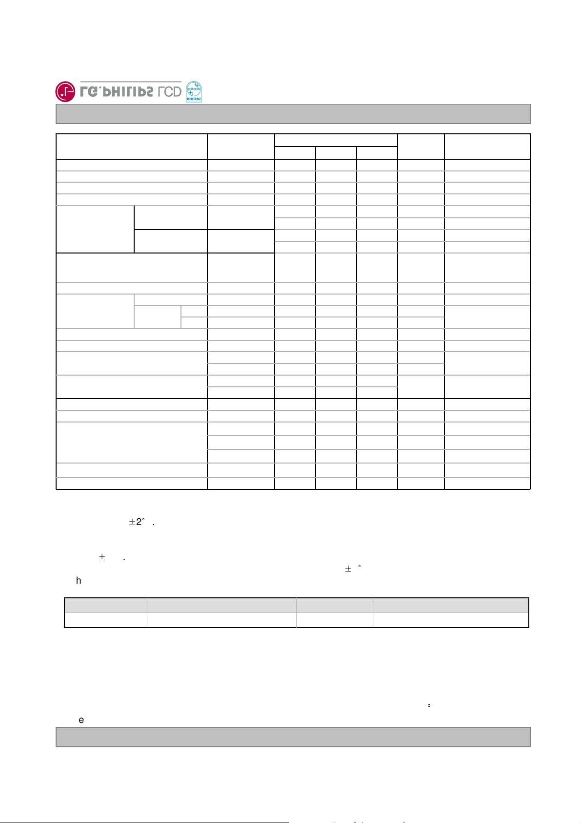
3-2. Interface Connections
This LCD module employs two kinds of interface connection, a 30-pin connector is used for the module
electronics and Master 14-pin and Slave 12-pin connectors are used for the integral backlight system.
3-2-1. LCD Module
- LCD Connector(CN1) : FI-X30SSL-HF (Manufactured by JAE) or Equivalent
- Mating Connector : FI-30C2L (Manufactured by JAE) or Equivalent
Table 4. MODULE CONNECTOR(CN1) PIN CONFIGURATION
NoteDescriptionSymbolPin No.
1
2
3
4
5
6
7
8
9
10
11
12
13
14
15
16
17
18
19
20
21
22
23
24
25
26
27
28
29
30
Note:
1. The pin no 9 is an option pin for DISM or LG format.( LG Format = “GND”or“OPEN”/ DISM Format =“VCC”)
Please refer to page 9 ,10 and 30 for further details.
2. The pin no 10 is an option pin for DCR Function ( Enable = “VCC” / Disable =“GND”)
3. The pin no 30 is LCD Test option.
“AGP” (Auto Generation LCM operates Pattern) or “NSB” (No Signal Black) is case that LVDS signals
are out of frequency or abnormal condition in spite of 12 volt power supply.
LPL recommends “NSB”. ( AGP : “VCC” or “OPEN” / NSB : “GND” )
4. All GND (ground) pins should be connected together, which should be also connected to the LCD
module’s metal frame.
5. All V
LCD
(power input) pins should be connected together.
6. Input Levels of LVDS signals are based on the IEA 664 Standard.
VLCD Power Supply +12.0V
Power Supply +12.0VVLCD
Power Supply +12.0VVLCD
Power Supply +12.0VVLCD
GroundGND
GroundGND
GroundGND
GroundGND
Select LVDS Data formatSelect
No ConnectionReserved(NC)
GroundGND
LVDS Receiver Signal(-)RALVDS Receiver Signal(+)RA+
GroundGND
LVDS Receiver Signal(-)RBLVDS Receiver Signal(+)RB+
GroundGND
LVDS Receiver Signal(-)RCLVDS Receiver Signal(+)RC+
GroundGND
LVDS Receiver Clock Signal(-)RCLKLVDS Receiver Clock Signal(+)RCLK+
GroundGND
LVDS Receiver Signal(-)RD-
LVDS Receiver Signal(+)RD+
GroundGND
No ConnectionReserved(NC)
No ConnectionReserved(NC)
GroundGND
GroundGND
1
2
3
Ver. 1.0 Dec. 15, 2006
8 / 28
Page 9
LC420WX5
Liquid Crystal Display
Product Specification
Table 5. REQUIRED SIGNAL ASSIGNMENT FOR LVDS TRANSMITTER (Pin9=“Low”or “OPEN”)
Host System
24 Bit
RED0
RED1
RED2
RED3
RED4
RED5
RED6
RED7
GREEN0
GREEN1
GREEN2
GREEN3
GREEN4
GREEN5
GREEN6
GREEN7
BLUE0
BLUE1
BLUE2
BLUE3
BLUE4
BLUE5
BLUE6
BLUE7
Hsync
Vsync
Data Enable
CLOCK
DS90C385
or Compatible
51
52
54
55
56
3
50
2
4
6
7
11
12
14
8
10
15
19
20
22
23
24
16
18
27
28
30
31
TxOUT0TxOUT0+
TxOUT1TxOUT1+
TxOUT2TxOUT2+
TxCLKOUTTxCLKOUT+
TxOUT3TxOUT3+
FI-X30SSL-HF
48
47
46
45
42
41
40
39
38
37
GND
GND
12
13
15
16
18
19
21
22
24
25
30
Timing
Controller
100
ΩΩΩΩ
100
ΩΩΩΩ
100
ΩΩΩΩ
100
ΩΩΩΩ
100
ΩΩΩΩ
9
RxIN0RxIN0+
RxIN1RxIN1+
RxIN2RxIN2+
RxCLKINRxCLKIN+
RxIN3RxIN3+
LG
/ DISM
LCD Test
LCD Module
Note: 1. The LCD Module uses a 100 Ohm[Ω] resistor between positive and negative lines of each receiver
input.
2. Refer to LVDS Transmitter Data Sheet for detail descriptions. (DS90C385 or Compatible)
3. ‘7’ means MSB and ‘0’ means LSB at R,G,B pixel data.
Ver. 1.0 Dec. 15, 2006
9 / 28
Page 10
Liquid Crystal Display
Product Specification
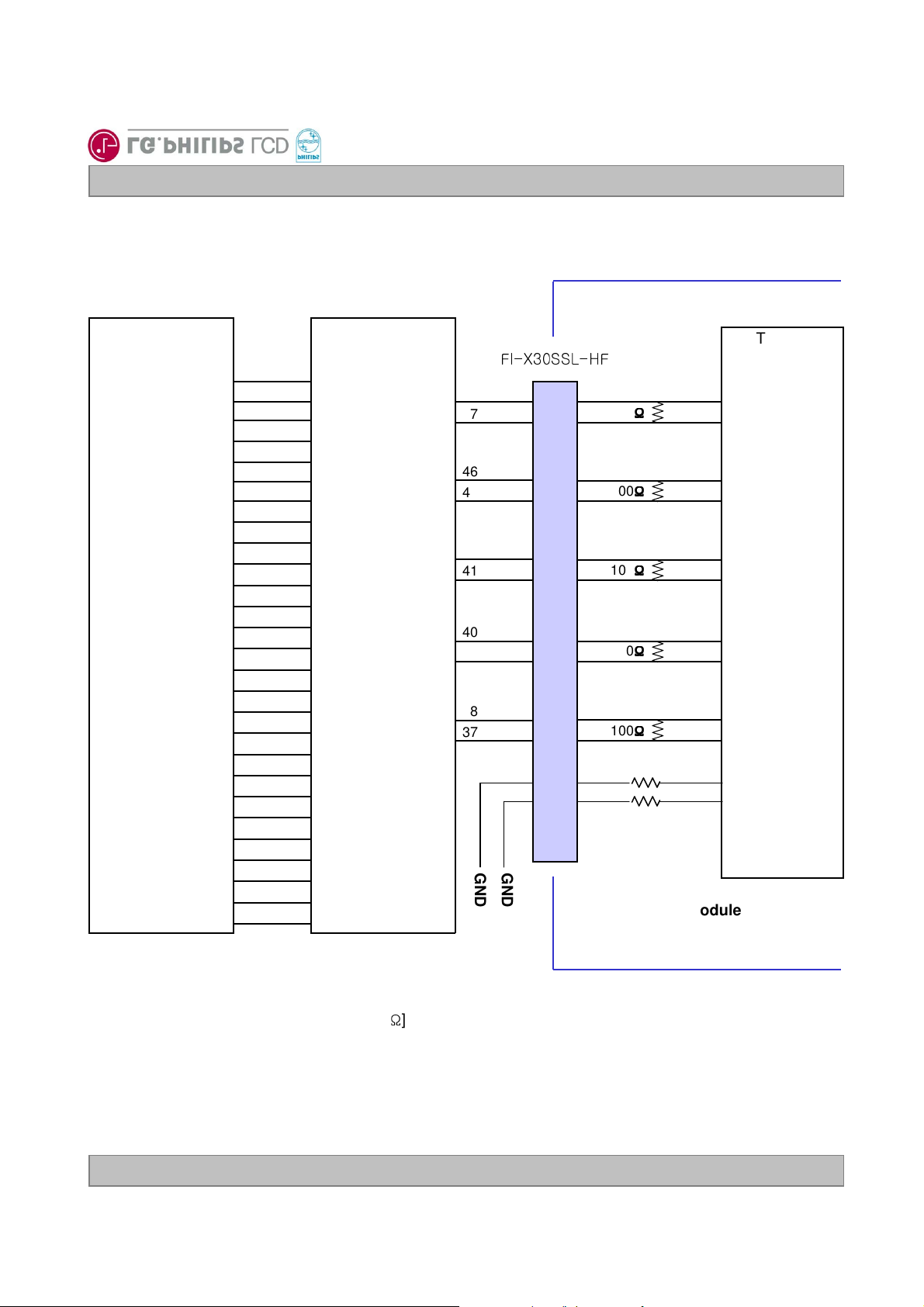
Table 6. REQUIRED SIGNAL ASSIGNMENT FOR LVDS TRANSMITTER ( Pin9=“High” )
LC420WX5
Host System
24 Bit
RED0
RED1
RED2
RED3
RED4
RED5
RED6
RED7
GREEN0
GREEN1
GREEN2
GREEN3
GREEN4
GREEN5
GREEN6
GREEN7
BLUE0
BLUE1
BLUE2
BLUE3
BLUE4
BLUE5
BLUE6
BLUE7
Hsync
Vsync
Data Enable
CLOCK
DS90C385
or Compatible
50
2
51
52
54
55
56
3
8
10
4
6
7
11
12
14
16
18
15
19
20
22
23
24
27
28
30
31
TxOUT0TxOUT0+
TxOUT1TxOUT1+
TxOUT2TxOUT2+
TxCLKOUTTxCLKOUT+
TxOUT3TxOUT3+
FI-X30SSL-HF
48
47
46
45
42
41
40
39
38
37
GND
Vcc
12
13
15
16
18
19
21
22
24
25
30
Timing
Controller
100
ΩΩΩΩ
100
ΩΩΩΩ
100
ΩΩΩΩ
100
ΩΩΩΩ
100
ΩΩΩΩ
9
RxIN0RxIN0+
RxIN1RxIN1+
RxIN2RxIN2+
RxCLKINRxCLKIN+
RxIN3RxIN3+
LG /
DISM
LCD Test
LCD Module
Note: 1. The LCD module uses a 100 Ohm[Ω] resistor between positive and negative lines of each receiver
input.
2. Refer to LVDS Transmitter Data Sheet for detail descriptions. (DS90C385 or Compatible)
3. ‘7’ means MSB and ‘0’ means LSB at R,G,B pixel data.
Ver. 1.0 Dec. 15, 2006
10 / 28
Page 11

Product Specification
3-2-2. Backlight Inverter
Master
-Inverter Connector : S14B-PH-SMC
(manufactured by JST) or Equivalent
- Mating Connector : PHR-14 or Equivalent
Table 7. INVERTER CONNECTOR PIN CONFIGULATION
1
2
3
4
5
BL
BL
BL
BL
BL
Power Supply +24.0VV
Power Supply +24.0VV
Power Supply +24.0VV
Power Supply +24.0VV
Power Supply +24.0VV
Slave
-Inverter Connector : S12B-PH-SMC
-Mating Connector : PHR-12 or Equivalent
Master
V
BL
V
BL
V
BL
V
BL
V
BL
LC420WX5
Liquid Crystal Display
(manufactured by JST) or Equivalent
Slave
V
BL
V
BL
V
BL
V
BL
V
BL
NoteDescriptionSymbolPin No
6
7
8
9
10
11
12
13
GND
GND
GND
GND
GND
ON/OFF
Backlight Ground
Backlight Ground
Backlight Ground
Backlight Ground
Backlight Ground
0.0V ~ 3.3VBoost
0.0V ~ 3.3VEXTVBR-
B
GND
GND
GND
GND
GND
BR
External PWM
14
Note : 1. GND should be connected to the LCD module’s metal frame.
2. Minimum Brightness : Boost = 0.0V Maximum Brightness : Boost = 3.3V
“OPEN” : Boost = 1.65V
3. Rising Edge : Lamp “ON” / Falling Edge : Lamp “OFF”
4. Pin#13 can be opened. ( if Pin #13 is open , EXTVBR-B is 100% )
5. Pin#14 can be opened. (Even though Pin #14 is GND or no connection, there is no effect on inverter operating)
6.
Each impedance of pin #11, 12 and 13 is 140
[KΩ]
, 400
[KΩ]
◆◆◆◆ Rear view of LCM
PCB
and 330
GND
GND
GND
GND
GND
Don’t careOn/Off0.0V ~ 5.0VV
[KΩ].
1
2Don’t careV
3, Open/High for B/L
on as default
-
4
5-GNDPOWER GNDGND
PCB
14
…
…
1
<Master>
Ver. 1.0 Dec. 15, 2006
1
…
…
12
<Slave>
11 / 28
Page 12

LC420WX5
Liquid Crystal Display
Product Specification
3-3. Signal Timing Specifications
Table 8 shows the signal timing required at the input of the LVDS transmitter. All of the interface signal timing
should be satisfied with the following specification for normal operation.
Table 8. TIMING TABLE for NTSC &PAL
CLK
HP
HV
WH
HBP
HFP
VP
VV
DCLK
Hsync
Period
Period
Horizontal Valid
Horizontal Blank
Frequency
Width
Horizontal Back Porch
Horizontal Front Porch
Period
Vertical Valid
[ DE (Data Enable) Only ]
NoteUnitMaxTypMinSymbolITEM
ns15.813.812.5t
MHz8072.463-Frequency
t
192015281456t
136613661366t
-
H
HP-tHV
162t
t
HP-tHV
5047.445f
-32-t
-4824t
-8040t
1063790776t
768768768t
CLK
t
CLK
KHz
t
CLK
t
t
HP
HP
t
HP
Hz636047f
t
HP
Hz-155t
t
HP
Vsync
Frequency
Width
Vertical Back Porch
Vertical Front Porch
-Vertical Blank
V
WV
VBP
VFP
VP-tVV
t
22t
VP-tVV
-5-t
-21t
Note :
1. The performance of the electro-optical characteristics may be influenced by variance of the vertical
refresh rate.
2. Above Timing Tables are only valid for DE Mode.
Ver. 1.0 Dec. 15, 2006
Note 1)
PAL : 47~53Hz
NTSC : 57~63Hz
12 / 28
Page 13

3-4. Signal Timing Waveforms
LC420WX5
Liquid Crystal Display
Product Specification
DCLK
First data
Second data
t
CLK
0.5 VDD
Invalid data
Invalid data
DE(Data Enable)
DE, Data
Pixel 0,0
Pixel 1,0
0.7VDD
Valid data
Pixel 2,0
Valid data
Pixel 3,0
0.3VDD
t
HV
Invalid data
Invalid data
t
DE(Data Enable)
Ver. 1.0 Dec. 15, 2006
HP
1 768
t
VV
t
VP
13 / 28
Page 14

LC420WX5
Liquid Crystal Display
Product Specification
3-5. Color Data Reference
The brightness of each primary color(red,green,blue) is based on the 8-bit gray scale data input for the color.
The higher binary input, the brighter the color. Table 9 provides a reference for color versus data input.
Table 9. COLOR DATA REFERENCE
Input Color Data
Basic
Color
RED
Color
Black 0 0 0 0 0 0 0 00 0 0 0 0 0 0 00 0 0 0 0 0 0 0
Red (255)
Green (255)
Blue (255)
Cyan
Magenta
Yellow
White
MSB LSB
RED
GREEN
MSB LSB
BLUE
MSB LSB
B7 B6 B5 B 4 B3 B2 B 1 B0G7 G6 G5 G4 G3 G2 G1 G0R7 R6 R5 R4 R3 R2 R1 R0
0 0 0 0 0 0 0 00 0 0 0 0 0 0 01 1 1 1 1 1 1 1
0 0 0 0 0 0 0 01 1 1 1 1 1 1 10 0 0 0 0 0 0 0
1 1 1 1 1 1 1 10 0 0 0 0 0 0 00 0 0 0 0 0 0 0
1 1 1 1 1 1 1 11 1 1 1 1 1 1 10 0 0 0 0 0 0 0
1 1 1 1 1 1 1 10 0 0 0 0 0 0 01 1 1 1 1 1 1 1
0 0 0 0 0 0 0 01 1 1 1 1 1 1 11 1 1 1 1 1 1 1
1 1 1 1 1 1 1 11 1 1 1 1 1 1 11 1 1 1 1 1 1 1
0 0 0 0 0 0 0 00 0 0 0 0 0 0 00 0 0 0 0 0 0 0RED (000) Dark
0 0 0 0 0 0 0 00 0 0 0 0 0 0 00 0 0 0 0 0 0 1RED (001)
............
0 0 0 0 0 0 0 00 0 0 0 0 0 0 01 1 1 1 1 1 1 0RED (254)
0 0 0 0 0 0 0 00 0 0 0 0 0 0 01 1 1 1 1 1 1 1RED (255)
0 0 0 0 0 0 0 00 0 0 0 0 0 0 00 0 0 0 0 0 0 0GREEN (000) Dark
GREEN
BLUE (000) Dark
BLUE
Ver. 1.0 Dec. 15, 2006
0 0 0 0 0 0 0 00 0 0 0 0 0 0 10 0 0 0 0 0 0 0GREEN (001)
............
0 0 0 0 0 0 0 01 1 1 1 1 1 1 00 0 0 0 0 0 0 0GREEN (254)
0 0 0 0 0 0 0 01 1 1 1 1 1 1 10 0 0 0 0 0 0 0GREEN (255)
0 0 0 0 0 0 0 00 0 0 0 0 0 0 00 0 0 0 0 0 0 0
0 0 0 0 0 0 0 10 0 0 0 0 0 0 00 0 0 0 0 0 0 0BLUE (001)
............
1 1 1 1 1 1 1 00 0 0 0 0 0 0 00 0 0 0 0 0 0 0BLUE (254)
1 1 1 1 1 1 1 10 0 0 0 0 0 0 00 0 0 0 0 0 0 0BLUE (255)
14 / 28
Page 15

3-6. Power Sequence
3-6-1. LCD Driving circuit
Power Supply For LCD
V
LCD
0V
Product Specification
90% 90%
10%
T1T
2
T5T
LC420WX5
Liquid Crystal Display
10%
6
T
7
Interface Signal (Tx)
Option Signal
(DISM, DCR_Enable)
Power for Lamp
Table 10. POWER SEQUENCE
Parameter
Valid Data
T
3
T
8
T
4
T
9
Lamp ON
Value
MaxTypMin
--200T4
Unit
ms10-0.5T1
ms50-0.5T2
ms--200T3
ms
ms50-0.5T5
ms300-0.01T6
s--1.0T7
ms0 < T8 < T2T8
ms0 < T9 < T5T9
Note : 1. Please avoid floating state of interface signal at invalid period.
2. When the interface signal is invalid, be sure to pull down the power supply V
3. The case when the T2/T5 exceed maximum specification, it operates protection
pattern(Black pattern) till valid signal inputted. There is no reliability problem.
4. The T3/T4 is recommended value, the case when failed to meet a minimum specification,
abnormal display would be shown. There is no reliability problem.
5. If the on time of option signal(DISM or DCR_Enable) precedes the on time of Power(VLCD),check
the LCD logic Power(Vcc) is under 0.8V, otherwise it will be happened abnormal display.
6. Flicker would come out when power on-off(T7=under 1s) is continuously tested over several ten-times
Ver. 1.0 Dec. 15, 2006
LCD
to 0V.
15 / 28
Page 16

3-6-2. Sequence for Inverter
LC420WX5
Liquid Crystal Display
Product Specification
Power Supply For Inverter
V
BL
10%
0V
V
ON/OFF
Boost
EXTV
BR-B
: 1. Lamp ON at PWM Rising Edge and Lamp OFF at PWM Falling Edge.
2. EXTVBR-B has Same sequence with Boost
3-6-3. Deep condition for Inverter
24V (typ.)
90%
0.7V
T1 T2 T3 T2
1000ms (Min) 1000ms (Min)
T4
T5
Lamp ON
T7
T6
T4
V
: 24V
BL
VBL(Typ.) x 0.85
Table 11. Power Sequence for Inverter
Parameter
Values
MaxTypMin
-
Units
ms--20T1
ms--500T2
ms--200T3
ms--10T5
Notes : 1. T1 describes rising time of 0V to 24V and is not applied at restarting time.
2. T4(max) is less than T2.
3. In T7 section, EXTV
BR-B
should be duty 100%.
4. When VBL[24V] is supplied always, there is no reliability problem.
Ver. 1.0 Dec. 15, 2006
0 V
Remarks
1
2ms0T4
VBL(Typ) x 0.85ms10--T6
3ms--1000T7
16 / 28
Page 17

LC420WX5
Liquid Crystal Display
Product Specification
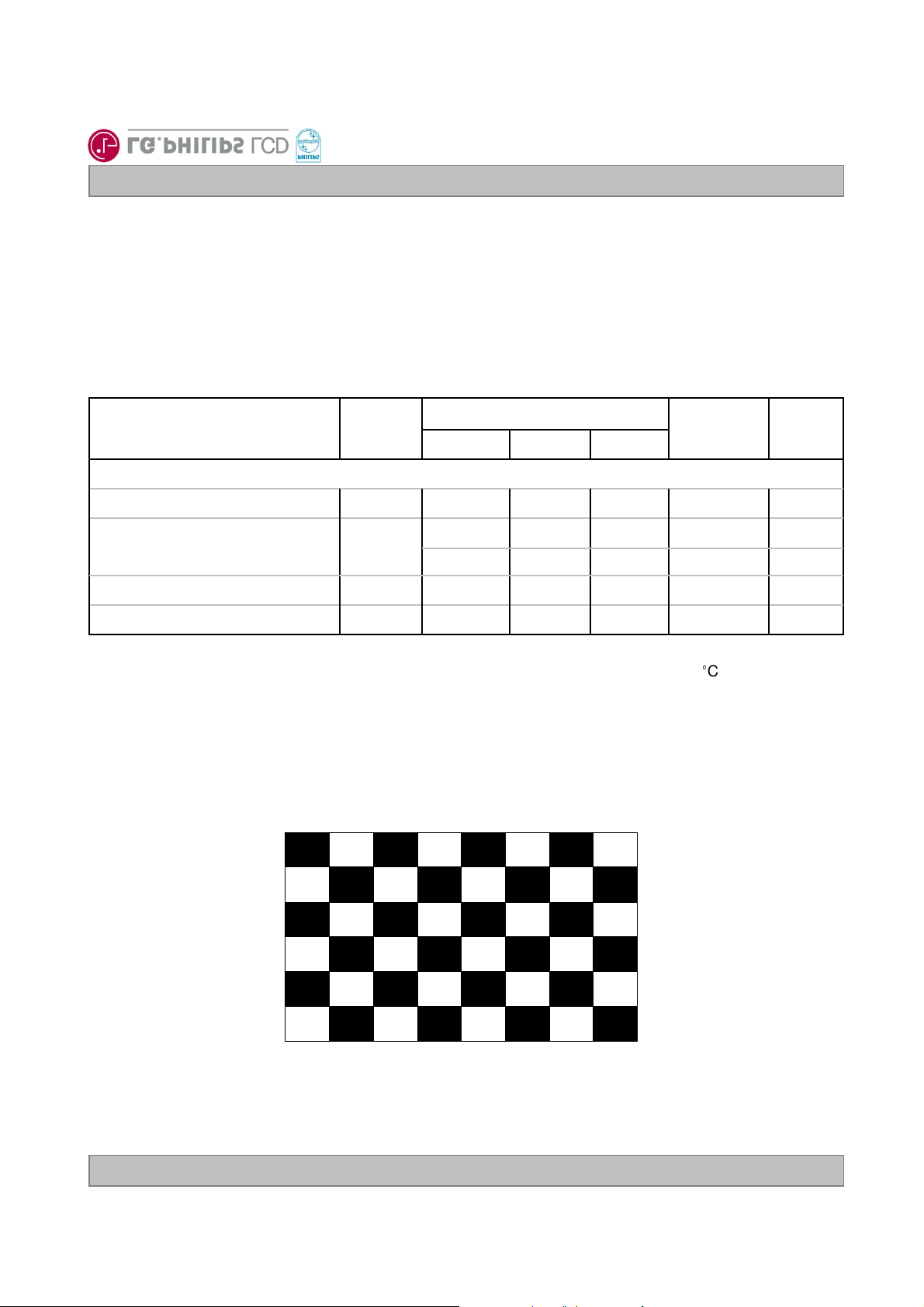
4. Optical Specification
Optical characteristics are determined after the unit has been ‘ON’ and stable in a dark environment at
25±2°C. The values are specified at an approximate distance 50cm from the LCD surface at a viewing angle
of Φ and θ equal to 0 °.
It is presented additional information concerning the measurement equipment and method in FIG. 1.
Optical Stage(x,y)
LCD Module
FIG. 1 Optical Characteristic Measurement Equipment and Method
Table 12. OPTICAL CHARACTERISTICS
SymbolParameter
Surface Luminance, white
Luminance Variation
Response Time
Color Coordinates
[CIE1931]
Viewing Angle (CR>10)
x axis, right(φ=0°)
x axis, left (φ=180°)
y axis, up (φ=90°)
y axis, down (φ=270°)
Gray-to-Gray
Rise + decay
RED
GREEN
BLUE
WHITE
WH
WHITE
BLACK
R +
Rx
Tr
Pritchard 880 or
equivalent
50cm
Ta= 25
±2°
C
, V
=12.0V, fV=60Hz, Dclk=72.4MHz, Boost=1.65V
LCD
Value
MaxTypMin
500400L
2
1.35Pδ
5P
1.7δ
85-G to G
D
1410-Tr
0.635
0.344Ry
0.286Gx
Typ
-0.03
0.614Gy
0.146Bx
Typ
+0.03
0.061By
0.279Wx
0.292Wy
-8985θr
-8985θl
-8985θu
-8985θd
NoteUnit
11000800CRContrast Ratio
2cd/m
3
4ms
5degree
6-2.2-Gray Scale
Ver. 1.0 Dec. 15, 2006
17 / 28
Page 18

Note :
LC420WX5
Liquid Crystal Display
Product Specification
1. Contrast Ratio(CR) is defined mathematically as :
Contrast Ratio =
Surface Luminance with all white pixels
Surface Luminance with all black pixels
It is measured at center 1-point.
2. Surface luminance is the luminance value at center 1-point across the LCD surface 50cm from the
surface with all pixels displaying white. For more information see the FIG. 2.
3. The variation in surface luminance , δ WHITE and δ BLACK are defined as :
δ WHITE(5P) = Maximum(L
δ BLACK(5P) = Maximum(L
Where L
on1
to L
are the luminance with all pixels displaying white at 5 locations .
on5
on1,Lon2
on1,Lon2
, L
, L
on3
on3
, L
, L
on4
on4
, L
) / Minimum(L
on5
, L
) / Minimum(L
on5
on1,Lon2
on1,Lon2
, L
, L
on3
on3
, L
, L
on4
on4
, L
, L
on5
on5
)
)
For more information, see the FIG. 2.
4. Response time is the time required for the display to transition from G(N) to G(M) (Rise Time, TrR)
and from G(M) to G(N) (Decay Time, TrD). For additional information see the FIG. 3. (N<M)
5. Viewing angle is the angle at which the contrast ratio is greater than 10. The angles are
determined for the horizontal or x axis and the vertical or y axis with respect to the z axis which
is normal to the LCD module surface. For more information, see the FIG. 4.
6. Gray scale specification
Gamma Value is approximately 2.2. For more information, see the Table 13.
Table 13. GRAY SCALE SPECIFICATION
Ver. 1.0 Dec. 15, 2006
Luminance [%] (Typ)Gray Level
0.11L0
0.19L15
1.08L31
2.07L47
4.51L63
7.75L79
12.05L95
17.06L111
22.36L127
28.21L143
35.56L159
43.96L175
53.00L191
63.37L207
74.66L223
88.17L239
100L255
18 / 28
Page 19

Product Specification
Measuring point for surface luminance & measuring point for luminance variation
H
A
③③③③②②②②
LC420WX5
Liquid Crystal Display
V
①①①①
B
A : H / 4 mm
④④④④
FIG.2 Measure Point for Luminance
Response time is defined as the following figure and shall be measured by switching the input signal for
“Gray(N)” and “Gray(M)”.
T
r
R
100
90
⑤⑤⑤⑤
T
r
D
B : V / 4 mm
H : 930.25 mm
V : 523.01 mm
@ H,V : Active Area
Optical
Response
10
0
Ver. 1.0 Dec. 15, 2006
Gray(N)
N,M = 0(Black)~255(White), N<M
FIG.3 Response Time
Gray(M)
Gray(N)
19 / 28
Page 20

Dimension of viewing angle range
LC420WX5
Liquid Crystal Display
Product Specification
φ
= 180°, Left
φ
= 270°, Down
Normal
θ
φ
FIG.4 Viewing Angle
E
Y
φ
= 90°, Up
φ
= 0°, Right
Ver. 1.0 Dec. 15, 2006
20 / 28
Page 21

LC420WX5
Liquid Crystal Display
Product Specification
5. Mechanical Characteristics
The contents provide general mechanical characteristics. In addition the figures in the next page are detailed
mechanical drawing of the LCD module.
Table 14. MECHANICAL CHARACTERISTICS
ValueItem
983.0 mmHorizontal
Outline Dimension
Bezel Area
Active Display Area
Surface Treatment
11.5 Kg (Typ.) , 12.5Kg (Max.) Weight
Hard coating(3H)
Anti-glare treatment of the front polarizer (Haze 13%)
576.0 mmVertical
51.0 mmDepth
939.0 mmHorizontal
531.0 mmVertical
930.25 mmHorizontal
523.01 mmVertical
Note : Please refer to page22 and 23 for mechanic drawings in terms of tolerance.
Ver. 1.0 Dec. 15, 2006
21 / 28
Page 22

<FRONT VIEW>
LC420WX5
Liquid Crystal Display
Product Specification
Ver. 1.0 Dec. 15, 2006
22 / 28
Page 23

<REAR VIEW>
LC420WX5
Liquid Crystal Display
Product Specification
Ver. 1.0 Dec. 15, 2006
23 / 28
Page 24

Product Specification
6. Reliability
Table 15. ENVIRONMENT TEST CONDITION
5
Vibration test
(operating)
LC420WX5
Liquid Crystal Display
ConditionTest ItemNo.
Ta= 50°C 240hHigh temperature storage test1
Ta= -20°C 240hLow temperature storage test2
Ta= 50°C 50%RH 240hHigh temperature operation test3
Ta= 0°C 240hLow temperature operation test4
Wave form : random
Vibration level : 1.0Grms
Bandwidth : 10-300Hz
Duration : X,Y,Z, 30 min
One time each direction
Shock level : 50Grms
6
8
Shock test
(operating)
Altitude operating
storage / shipment
Waveform : half sine wave, 11ms
Direction :±X, ±Y, ±Z
One time each direction
°
Ta= 40
0 - 14,000 feet(4267.2m)
0 - 40,000 feet(12192m)
C ,90%RHHumidity condition Operation7
Ver. 1.0 Dec. 15, 2006
24 / 28
Page 25

LC420WX5
Liquid Crystal Display
Product Specification
7. International standards
7-1. Safety
a) UL 60065, 7thEdition, dated June 30, 2003, Underwriters Laboratories, Inc.,
Standard for Audio, Video and Similar Electronic Apparatus.
b) CAN/CSA C22.2, No. 60065:03, Canadian Standards Association,
Standard for Audio, Video and Similar Electronic Apparatus.
c) IEC60065:2001, 7thEdition CB-scheme and EN 60065:2002,
Safety requirements for Audio, Video and Similar Electronic Apparatus..
7-2. EMC
a) ANSI C63.4 “Methods of Measurement of Radio-Noise Emissions from Low-Voltage Electrical and
Electrical Equipment in the Range of 9kHZ to 40GHz. “American National Standards Institute(ANSI),
1992
b) C.I.S.P.R “Limits and Methods of Measurement of Radio Interface Characteristics of Information
Technology Equipment.“ International Special Committee on Radio Interference.
c) EN 55022 “Limits and Methods of Measurement of Radio Interface Characteristics of Information
Technology Equipment.“ European Committee for Electrotechnical Standardization.(CENELEC), 1998
( Including A1: 2000 )
Ver. 1.0 Dec. 15, 2006
25 / 28
Page 26

Product Specification
8. Packing
8-1. Designation of Lot Mark
a) Lot Mark
A B C D E F G H I J K L M
A,B,C : SIZE(INCH) D : YEAR
E : MONTH F : FACTORY CODE
G ~ M : SERIAL NO.
Note
1. YEAR
LC420WX5
Liquid Crystal Display
Year
Mark
321
200452005
4
200320022001
2006720078200892009
6
2. MONTH
Month
Mark
Apr5May
4
Jun7Jul8Aug9Sep
6
b) Location of Lot Mark
Serial No. is printed on the label. The label is attached to the backside of the LCD module.
This is subject to change without prior notice.
2010
0
Oct
A
Nov
B
DecMarFebJan
C321
8-2. Packing Form
a) Package quantity in one box : 12 pcs
b) Box Size :1150 mm X 1020 mm X 815 mm.
Ver. 1.0 Dec. 15, 2006
26 / 28
Page 27

LC420WX5
Liquid Crystal Display
Product Specification
9. Precautions
Please pay attention to the followings when you use this TFT LCD module.
9-1. Mounting Precautions
(1) You must mount a module using holes arranged in four corners or four sides.
(2) You should consider the mounting structure so that uneven force (ex. Twisted stress) is not applied to the
module. And the case on which a module is mounted should have sufficient strength so that external
force is not transmitted directly to the module.
(3) Please attach the surface transparent protective plate to the surface in order to protect the polarizer.
Transparent protective plate should have sufficient strength in order to the resist external force.
(4) You should adopt radiation structure to satisfy the temperature specification.
(5) Acetic acid type and chlorine type materials for the cover case are not desirable because the former
generates corrosive gas of attacking the polarizer at high temperature and the latter causes circuit break
by electro-chemical reaction.
(6) Do not touch, push or rub the exposed polarizers with glass, tweezers or anything harder than HB
pencil lead. And please do not rub with dust clothes with chemical treatment.
Do not touch the surface of polarizer for bare hand or greasy cloth.(Some cosmetics are detrimental
to the polarizer.)
(7) When the surface becomes dusty, please wipe gently with absorbent cotton or other soft materials like
chamois soaks with petroleum benzine. Normal-hexane is recommended for cleaning the adhesives
used to attach front / rear polarizers. Do not use acetone, toluene and alcohol because they cause
chemical damage to the polarizer.
(8) Wipe off saliva or water drops as soon as possible. Their long time contact with polarizer causes
deformations and color fading.
(9) Do not open the case because inside circuits do not have sufficient strength.
9-2. Operating Precautions
(1) The spike noise causes the mis-operation of circuits. It should be lower than following voltage :
V=±200mV(Over and under shoot voltage)
(2) Response time depends on the temperature.(In lower temperature, it becomes longer.)
(3) Brightness depends on the temperature. (In lower temperature, it becomes lower.)
And in lower temperature, response time(required time that brightness is stable after turned on) becomes
longer.
(4) Be careful for condensation at sudden temperature change. Condensation makes damage to polarizer or
electrical contacted parts. And after fading condensation, smear or spot will occur.
(5) When fixed patterns are displayed for a long time, remnant image is likely to occur.
(6) Module has high frequency circuits. Sufficient suppression to the electromagnetic interference shall be
done by system manufacturers. Grounding and shielding methods may be important to minimized the
interference.
(7) Please do not give any mechanical and/or acoustical impact to LCM. Otherwise, LCM can’t be operated
its full characteristics perfectly.
(8) A screw which is fastened up the steels should be a machine screw.
(if not, it causes metallic foreign material and deal LCM a fatal blow)
(9) Please do not set LCD module on its edge.
Ver. 1.0 Dec. 15, 2006
27 / 28
Page 28

LC420WX5
Liquid Crystal Display
Product Specification
9-3. Electrostatic Discharge Control
Since a module is composed of electronic circuits, it is not strong to electrostatic discharge. Make certain that
treatment persons are connected to ground through wrist band etc. And don’t touch interface pin directly.
9-4. Precautions for Strong Light Exposure
Strong light exposure causes degradation of polarizer and color filter.
9-5. Storage
When storing modules as spares for a long time, the following precautions are necessary.
(1) Store them in a dark place. Do not expose the module to sunlight or fluorescent light. Keep the temperature
between 5°C and 35°C at normal humidity.
(2) The polarizer surface should not come in contact with any other object.
It is recommended that they be stored in the container in which they were shipped.
9-6. Handling Precautions for Protection Film
(1) The protection film is attached to the bezel with a small masking tape.
When the protection film is peeled off, static electricity is generated between the film and polarizer.
This should be peeled off slowly and carefully by people who are electrically grounded and with well ionblown equipment or in such a condition, etc.
(2) When the module with protection film attached is stored for a long time, sometimes there remains a very
small amount of glue still on the bezel after the protection film is peeled off.
(3) You can remove the glue easily. When the glue remains on the bezel surface or its vestige is recognized,
please wipe them off with absorbent cotton waste or other soft material like chamois soaked with normalhexane.
Ver. 1.0 Dec. 15, 2006
28 / 28
Page 29

Appendix A : Black Level and Black Uniformity
This is only the reference data of black level and black uniformity for LC420WX5-SLD1 model.
1. Black Level :
Surface Luminance of Black (L
2. Black Uniformity
The variation of surface luminance of black , δ
δ BLACK = Maximum(L
3. Sampling Size : 5 pcs
4. Measurement Method : Follow the same rule as optical characteristics measurement.
5. Measurement location: refer to below.
on1,Lon2
BLACK
) is the luminance value at center 1-point.
BLACK
is defined as :
, L
, L
, L
on3
on4
H
A
) / Minimum(L
on5
on1,Lon2
, L
on3
, L
on4
, L
on5
)
③②
V
B
④
①
⑤
A : H / 4 mm
B : V / 4 mm
H : 930.25 mm
V : 523.01 mm
@ H,V : Active Area
6. Current Status
Below table is actual data of production on Dec. 08, 2006 ( LPL RV Event Sample)
No.
1
2
3
4
5
Luminance
0.52
0.53
0.53
0.51
0.54
Black Level
1.22
1.52
1.19
1.41
1.24
7. Black Level and Black Uniformity Control Method
-. LPL will continue to monitor the quality level of mass production regularly in terms of black level and black
uniformity.
Page 30

Appendix B : Option Pin Circuit Block Diagram
The figure of the option pin Circuit Block Diagram
1K
ΩΩΩΩ
Selector (Pin 9) Selector
50K
ΩΩΩΩ
System Side LCM Side
[ The Selector Pin Circuit Block Diagram ]
ASIC
(TCON)
Page 31

Appendix C : White Uniformity for PWM Duty 50%
This is only the reference data of white uniformity for LC420WX5-SLD1 model at the condition of PWM
Duty 50%.
1. White Uniformity
The variation of surface luminance of white , δ
δ WHITE = Maximum(L
on1,Lon2
, L
on3
, L
on4
2. Sampling Size : 5 pcs ( RV Typical Sample )
3. Measurement Method : Follow the same rule as optical characteristics measurement except PWM 50%
condition.
1) Boost level should be typical value. ( 1.65 Volt)
2) PWM 50% duty period should be measured at the inverter input connector #13 Pin.
4. Measurement location: refer to below.
WHITE
, L
) / Minimum(L
on5
is defined as :
on1,Lon2
, L
on3
, L
on4
, L
on5
)
H
A
③②
V
B
④
①
⑤
A : H / 4 mm
B : V / 4 mm
H : 930.25 mm
V : 523.01 mm
@ H,V : Active Area
5. Current Status
Below table is actual data of production on Dec. 14, 2006 ( LPL RV Event Sample)
Position
①
②
③
Luminance for PWM Duty 100%
# 1
505
475
476
# 2
497
467
459
# 3
501
468
484
# 4
506
471
474
# 5
493
480
484
Luminance for PWM Duty 50%
# 1
259
247
252
# 2
257
252
251
# 3 # 5
260
251
253
# 4
259
249
247
258
251
253
④
⑤
δ WHITE@5pts
497
1.080
506
1.102
513
1.105
511
1.085
487
1.054
253
1.049
260
1.04
258
1.04
261
1.06
260
257262259259256506505517498513
1.04
Page 32

Appendix D : Audible Noise Level
These are measurement method and condition of Audible Noise Level for LC420WX5-SLD1 model at worse
case conditions
1. Audible Noise Level target
-. Peak: Max. 24dB(A)
-. Overall: Max. 27dB(A)
2. Sample : RV Typical Sample(N=3)
3. Measurement Method and Target Value : Follow the rule
▶
Measurement Conditions
Type of room
Distance to display
Side
Background noise
▶
Measurement Equipment Properties and Settings
Frequency range
Measurement Step Width
Duration : For average
Weighted Filter ; (thus dB A Scale)
▶
Target Value at LCM Level
Overall Level ( if no peak frequency)
Peak Level each 1/3 octave
(between 800Hz-6KHz
Display specific conditions
Anechoic
1m (Typical)
Front @ Center
≤
18dB(A)
50Hz to 20KHz (Typical)
1/3 octave
60 sec (Typical)
A - type
Limit < 27 dB (A)
Limit < 24 dB (A)
Any worse case conditions
Page 33

# APPENDIX-ⅠⅠⅠⅠ
■LC420WX5-SLD1 – Pallet Ass’y
LC420WX5
Liquid Crystal Display
Product Specification
6
ANGLE PACKING7
ANGLE COVER8
Ver. 1.0 Dec. 15, 2006
LCD Module1
PACKING EPS5
PACKING
BAND,CLIP9
BAND10
LABEL11
MATERIALDESCRIPTIONNO.
42INCHBAG2
MASKING 20MM X 50MTAPE3
PAPER 1140X1000X138MMPALLET4
EPS
PAPER
PAPER
STEEL
PP
YUPO PAPER 80G 100X100
33 / 28
Page 34

LC420WX5
Liquid Crystal Display
# APPENDIX 2
Product Specification
# APPENDIX- ⅡⅡⅡⅡ
■ LCM Label
Model
LC420WX5
(SL)(D1)
RoHS Verified
Serial No.
UL, TUV Mark
LPL Logo
US PATENT No. Origin
■■■■ Serial No. (See CAS 26page for more information)
1 2 3 4 5 6 7 9 10 11 12
Inch
Ver. 1.0 Dec. 15, 2006
MonthYear
M Ass’y Factory code
8
13
Serial No.
34 / 28
Page 35

LC420WX5
Liquid Crystal Display
# APPENDIX 3
# APPENDIX- ⅢⅢⅢⅢ
■ Pallet Label
LC420WX5
12
Product Specification
SLD1
RoHS Verified
Ver. 1.0 Dec. 15, 2006
35 / 28
 Loading...