

LC370W01
Liquid Crystal Display
Product Specification
SPECIFICATION
FOR
APPROVAL
●
)
(
Preliminary Specification
)(
Final Specification
37.0” WXGA TFT LCDTitle
APPROVED BY
/
/
/
GeneralBUYER
-MODEL
SIGNATURE
DATE
LG.Philips LCD Co., Ltd.SUPPLIER
LC370W01*MODEL
A6SUFFIX
*When you obtain standard approval,
please use the above model name without suffix
APPROVED BY
Jay Yoon / G.Manager
REVIEWED BY
H.S. Song / Manager
PREPARED BY
S.S. Kim / Engineer
SIGNATURE
DATE
Please return 1 copy for your confirmation with
your signature and comments.
Ver. 0.0 Sep.15, 2004
TV Product Development Dept.
LG. Philips LCD Co., Ltd
1/ 28
Product Specification
Contents
LC370W01
Liquid Crystal Display
PageITEMNumber
COVER
CONTENTS
GENERAL DESCRIPTION1
ABSOLUTE MAXIMUM RATINGS2
ELECTRICAL SPECIFICATIONS3
ELECTRICAL CHARACTERISTICS3-1
INTERFACE CONNECTIONS3-2
SIGNAL TIMING SPECIFICATIONS3-3
SIGNAL TIMING WAVEFORMS3-4
COLOR INPUT DATA REFERENCE3-5
POWER SEQUENCE3-6
OPTICAL SPECIFICATIONS4
MECHANICAL CHARACTERISTICS5
RELIABILITY6
1
2
3RECORD OF REVISIONS
4
5
6
6
8
12
13
14
15
17
21
24
INTERNATIONAL STANDARDS7
SAFETY7-1
EMC7-2
PACKING8
DESIGNATION OF LOT MARK8-1
PACKING FORM8-2
Ver. 0.0 Sep.15, 2004
25
25
25
26
26
26
27PRECAUTIONS9
27MOUNTING PRECAUTIONS9-1
27OPERATING PRECAUTIONS9-2
28ELECTROSTATIC DISCHARGE CONTROL9-3
28PRECAUTIONS FOR STRONG LIGHT EXPOSURE9-4
28STORAGE9-5
28HANDLING PRECAUTIONS FOR PROTECTION FILM9-6
2/ 28
Product Specification
Record of Revisions
Preliminary Specification(First Draft)-Sep.15, 20040.0
LC370W01
Liquid Crystal Display
DescriptionPageRevision DateRevision No.
Ver. 0.0 Sep.15, 2004
3/ 28
LC370W01
Liquid Crystal Display
Product Specification
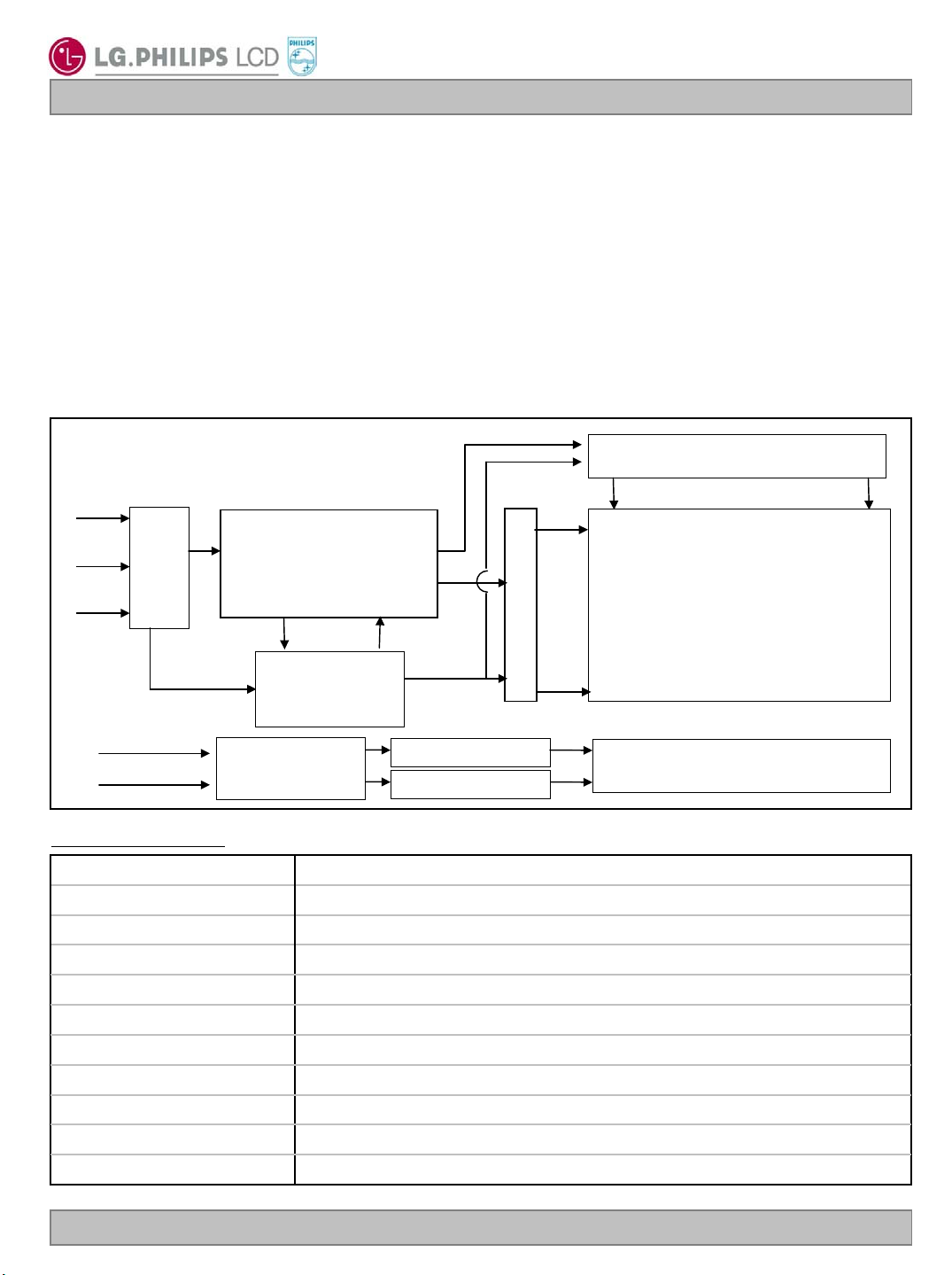
1. General Description
LC370W01 is a Color Active Matrix Liquid Crystal Display with an integral Cold Cathode Fluorescent
Lamp(CCFL) backlight system. The matrix employs a-Si Thin Film Transistor as the active element.
It is a transmissive type display operating in the normally black mode. It has a 37.02 inch diagonally
measured active display area with WXGA resolution (768 vertical by 1366 horizontal pixel array)
Each pixel is divided into Red, Green and Blue sub-pixels or dots which are arranged in vertical stripes.
Gray scale or the luminance of the sub-pixel color is determined with a 8-bit gray scale signal for each dot,
thus presenting a palette of more than 16.7M(true) colors.
It has been designed to apply the 8-bit 1 port LVDS interface.
It is intended to support LCD TV, PCTV where high brightness, super wide viewing angle, high color gamut,
high color depth and fast response time are important.
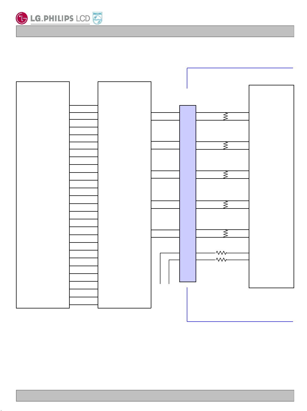
RGB
Source Driver Circuit
S1 S1366
G1
+12.0V
LVDS
5pair
Option
# 9
CN1
(30pin)
Timing Controller
(LVDS Rx integrated)
Gate Driver Circuit
TFT - LCD Panel
(1366 × RGB × 768 pixels)
+24.0V
GND
General Features
Power Circuit
Block
Inverter
(CN2,CN3,
12pin)
37.02 inches(940.3mm) diagonalActive Screen Size
877.0/878.0mm(H) x 516.8mm(V) x 55.5mm(D) (Typ.)Outline Dimension
0.200mm x 0.600mm x RGBPixel Pitch
1366 horiz. by 768 vert. pixels RGB stripe arrangementPixel Format
8-bit, 16.7 M colorsColor Depth
500 cd/m2 (Center 1 point Typ.)Luminance, White
Viewing angle free ( R/L 176(Typ.), U/D 176(Typ.))Viewing Angle (CR>10)
Total 125Watt (Typ.) (Logic=4.5W, Lamp=120W [IBL=6.0mA] )Power Consumption
11,500 (Typ.)Weight
Transmissive mode, normally blackDisplay Operating Mode
Hard coating(3H), Anti-glare treatment of the front polarizerSurface Treatment
G768
8CNs (High)
Back light Assembly (16CCFL)
8CNs (High)
Ver. 0.0 Sep.15, 2004
4/ 28
LC370W01
Liquid Crystal Display
Product Specification
2. Absolute Maximum Ratings
The followings are maximum values which, if exceeded, may cause faulty operation or damage to the unit.
Table 1. ABSOLUTE MAXIMUM RATINGS
Value
Parameter Remark
Symbol
Unit
MaxMin
Power Input
Voltage
LCM
VDC27.021.6VBLBacklight inverter
VDC5.25-0.30VON/OFFON/OFF Control Voltage
VDC3.30.0VBrBrightness Control Voltage
400TOPOperating Temperature
50-20TSTStorage Temperature
℃
℃
%RH9010HOPOperating Ambient Humidity
%RH9010HSTStorage Humidity
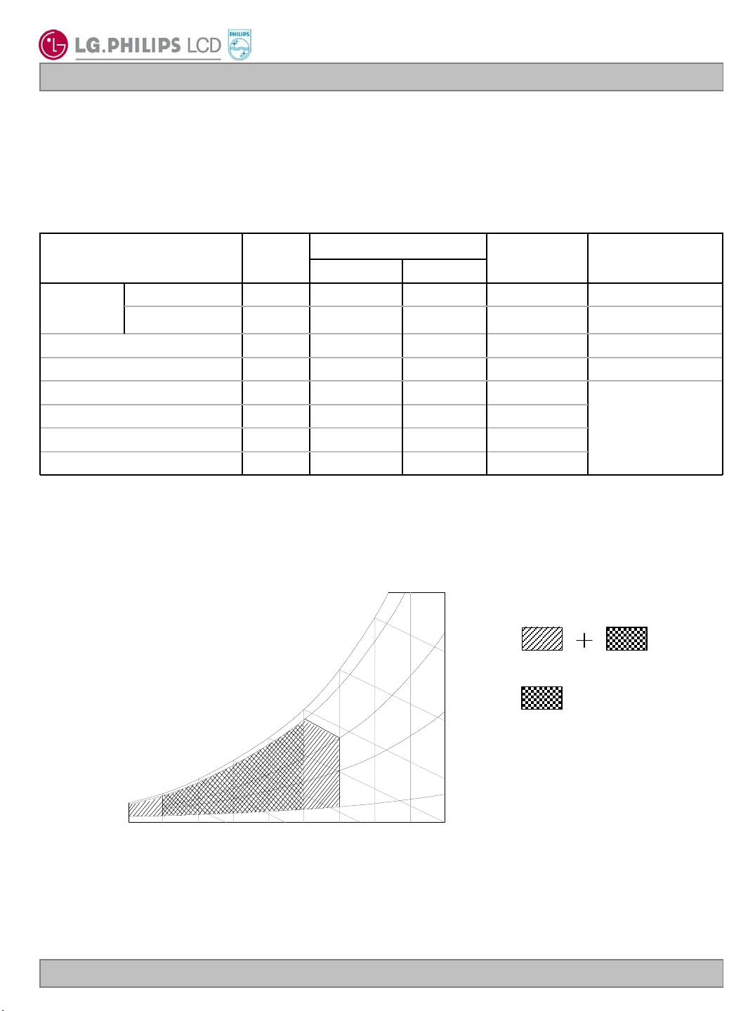
Note : 1. Temperature and relative humidity range are shown in the figure below.
Wet bulb temperature should be 39 °C Max. and no condensation of water.
90%
60
60%
at 25 ± 2 °CVDC14.0-0.3VLCD
Note 1
Wet Bulb
50
Temperature [℃]
40
30
20
10
0
10 20 30 40 50 60 70 800-20
Dry Bulb Temperature [°C]
Ver. 0.0 Sep.15, 2004
40%
10%
Storage
Operation
Humidity [(%)RH]
5/ 28
LC370W01
Liquid Crystal Display
Product Specification
3. Electrical Specifications
3-1. Electrical Characteristics
It requires two power inputs. One is employed to power the LCD electronics and to drive the TFT array and
liquid crystal. The other input power for the CCFL/Backlight is to power inverter.
Table 2_1. ELECTRICAL CHARACTERISTICS
Parameter Symbol
MODULE :
VLCDPower Input Voltage
VRPPermissible Input Ripple Voltage
Value
MaxTypMin
12.612.011.4
200--
430370310
ILCDPower Input Current
680510-
PLCDPower Consumption
IRUSHRush current
5.24.53.8
3.0--
Note :
1. The specified current and power consumption are under the V
whereas mosaic pattern(8 x 6) is displayed and f
is the frame frequency.
V
=12.0V, 25 ± 2°C, fV=60Hz condition
LCD
2. The current is specified at the maximum current pattern.
3. The duration of rush current is about 2ms and rising time of power Input is 1ms(min.).
White : 255Gray
Black : 0Gray
NoteUnit
VDC
mVP-P
1mA
2mA
1Watt
3A
Mosaic Pattern(8 x 6)
Ver. 0.0 Sep.15, 2004
6/ 28
Product Specification
Table 2_2. ELECTRICAL CHARACTERISTICS
LC370W01
Liquid Crystal Display
Parameter Symbol
NoteUnit
MaxTypMin
Inverter :
Value
Power Input Voltage
Power Input Voltage Ripple
Power Input Current
Power Consumption
Input Voltage for
Brightness Adjust
Control System
Signals
On/Off
BL
On
Off
VDC25.224.022.8VBL
Vp-p0.2--0.2
VDC5.255.004.00V on
DC0.50.0-0.3V off
V
1
1A6.55.0-IBL
1W156120-P
2VDC3.30VBR
Lamp :
Life Time
3Hrs50,000
Note :
1. Electrical characteristics are determined after the unit has been ‘ON’ and stable for approximately 120Min
at 25±2°C and
VBR = 3.3V.
The specified current and power consumption are under the typical supply Input voltage, 24.0V.
It is total power consumption.
2.
Brightness Control.
BR Voltage control brightness.
This V
VBR Voltage
Function
Maximum Brightness (100%)3.3V
Minimum Brightness.(15~25%)0V
3. The life time is determined as the time at which luminance of the lamp is 50% compared to that of initial
value at the typical lamp current on condition of continuous operating at 25 ± 2°C.
Specified value is when lamp is aligned horizontally.
Ver. 0.0 Sep.15, 2004
7/ 28
LC370W01
Liquid Crystal Display
Product Specification
3-2. Interface Connections
This LCD employs two kinds of interface connection, a 30-pin connector is used for the module electronics
and two 12-pin Connectors are used for the integral backlight system.
3-2-1. LCD Module
- LCD Connector(CN1) : FI-X30SSL-HF (Manufactured by JAE) or Equivalent
- Mating Connector : FI-X30C2L (Manufactured by JAE) or Equivalent
Table 3. MODULE CONNECTOR(CN1) PIN CONFIGURATION
NoteDescriptionSymbolPin No.
1
2
3
4
5
6
7
8
9
10
11
12
13
14
15
16
17
18
19
20
21
22
23
24
25
26
27
28
29
30
Note: 1. If the pin no. 9 is Ground, Interface format is “LG”, and if the pin no. 9 is Vcc(3.3V), Interface format
is “DISM”. See page 9 and 10.
2. The pin no. 30 is necessary for LCD test.
When LVDS signals are abnormal operation more than 3-Vsync times and power 12V is supplied,
‘Open’ or ‘Vcc’ : LCD operate itself some test patterns.(AGP – Auto Generation Pattern)
‘Ground’ : LCD operate itself a black pattern. (NSB – No Signal Black)
LPL recommend ‘Ground’ for NSB.
3. All GND (ground) pins should be connected together, which should be also connected to the LCD
module’s metal frame.
4. All V
LCD (power input) pins should be connected together.
5. Input Levels of LVDS signals are based on the IEA 664 Standard.
VLCD Power Supply +12.0V
Power Supply +12.0VVLCD
Power Supply +12.0VVLCD
Power Supply +12.0VVLCD
GroundGND
GroundGND
GroundGND
GroundGND
Select LVDS Data formatSelect
NCNC
GroundGND
LVDS Receiver Signal(-)RALVDS Receiver Signal(+)RA+
GroundGND
LVDS Receiver Signal(-)RBLVDS Receiver Signal(+)RB+
GroundGND
LVDS Receiver Signal(-)RC-
LVDS Receiver Signal(+)RC+
GND
Ground
LVDS Receiver Clock Signal(-)RCLK-
LVDS Receiver Clock Signal(+)RCLK+
GroundGND
LVDS Receiver Signal(-)RDLVDS Receiver Signal(+)RD+
GroundGND
NCNC
NCNC
GroundGND
LCD testNC(GND)
1
2
Ver. 0.0 Sep.15, 2004
8/ 28
Liquid Crystal Display
Product Specification
Table 4. REQUIRED SIGNAL ASSIGNMENT FOR LVDS TRANSMITTER ( Pin9=“L” or “Open” )
LC370W01
Host System
24 Bit
RED0
RED1
RED2
RED3
RED4
RED5
RED6
RED7
GREEN0
GREEN1
GREEN2
GREEN3
GREEN4
GREEN5
GREEN6
GREEN7
BLUE0
BLUE1
BLUE2
BLUE3
BLUE4
BLUE5
BLUE6
BLUE7
Hsync
Vsync
Data Enable
CLOCK
DS90C385
or Compatible
51
52
54
55
56
3
50
2
4
6
7
11
12
14
8
10
15
19
20
22
23
24
16
18
27
28
30
31
TxOUT0TxOUT0+
TxOUT1TxOUT1+
TxOUT2TxOUT2+
TxCLKOUTTxCLKOUT+
TxOUT3TxOUT3+
FI-X30SSL-HF
48
47
46
45
42
41
40
39
38
37
GND
GND
12
13
15
16
18
19
21
22
24
25
30
Timing
Controller
100Ω
100Ω
100Ω
100Ω
100Ω
9
RxIN0RxIN0+
RxIN1RxIN1+
RxIN2RxIN2+
RxCLKINRxCLKIN+
RxIN3RxIN3+
LG / DISM
LCD Test
LCD Module
Note: 1. The LCD Module uses a 100 Ohm[Ω] resistor between positive and negative lines of each receiver
input.
2. Refer to LVDS Transmitter Data Sheet for detail descriptions. (DS90C385 or Compatible)
3. ‘7’ means MSB and ‘0’ means LSB at R,G,B pixel data.
Ver. 0.0 Sep.15, 2004
9/ 28

Product Specification
Table 5. REQUIRED SIGNAL ASSIGNMENT FOR LVDS TRANSMITTER ( Pin9=“H” )
LC370W01
Liquid Crystal Display
Host System
24 Bit
RED0
RED1
RED2
RED3
RED4
RED5
RED6
RED7
GREEN0
GREEN1
GREEN2
GREEN3
GREEN4
GREEN5
GREEN6
GREEN7
BLUE0
BLUE1
BLUE2
BLUE3
BLUE4
BLUE5
BLUE6
BLUE7
Hsync
Vsync
Data Enable
CLOCK
DS90C385
or Compatible
50
2
51
52
54
55
56
3
8
10
4
6
7
11
12
14
16
18
15
19
20
22
23
24
27
28
30
31
TxOUT0TxOUT0+
TxOUT1TxOUT1+
TxOUT2TxOUT2+
TxCLKOUTTxCLKOUT+
TxOUT3TxOUT3+
FI-X30SSL-HF
48
47
46
45
42
41
40
39
38
37
GND
Vcc
12
13
15
16
18
19
21
22
24
25
30
Timing
Controller
100Ω
100Ω
100Ω
100Ω
100Ω
9
RxIN0RxIN0+
RxIN1RxIN1+
RxIN2RxIN2+
RxCLKINRxCLKIN+
RxIN3RxIN3+
LG /
DISM
LCD Test
LCD Module
Note: 1. The LCD Module uses a 100 Ohm[Ω] resistor between positive and negative lines of each receiver
input.
2. Refer to LVDS Transmitter Data Sheet for detail descriptions. (DS90C385 or Compatible)
3. ‘7’ means MSB and ‘0’ means LSB at R,G,B pixel data.
Ver. 0.0 Sep.15, 2004
10 / 28

Product Specification
3-2-2. Backlight Inverter
- Inverter Connector : S12B-PH-SM3(manufactured by JST) or Equivalent
- Mating Connector : PHR-12 or Equivalent
Table 6. INVERTER CONNECTOR PIN CONFIGULATION
LC370W01
Liquid Crystal Display
NoteDescriptionSymbolPin No
Power Supply +24.0VVBL
Power Supply +24.0VVBL
Power Supply +24.0VVBL
Power Supply +24.0VVBL
Power Supply +24.0VVBL
POWER GND
POWER GND
POWER GND
POWER GND
POWER GND
0V ~ 3.3V
0V ~ 5.0V
10
11
12
1
2
3
4
5
6
7
8
9
GND
GND
GND
GND
GND
BR
V
On/Off
Note :
1. GND is connected to the LCD module’s metal frame.
PCB
1 2
3
S12B-PH-SM3-TB
(JST : Japan Solderless Terminal Co.,Ltd.)
2. 0V : Minimum Brightness.
3.3V : Maximum Brightness.
10
11
1
2
3
12
3. On : 4.0 ~ 5.25V
Off : -0.3 ~ 0.5V
Ver. 0.0 Sep.15, 2004
11 / 28

LC370W01
Liquid Crystal Display
Product Specification
3-3. Signal Timing Specifications
This is the signal timing required at the input of LVDS Transmitter. All of the interface signal timing should be
satisfied with the following specifications for it’s proper operation.
Table 7. TIMMING TABLE
RemarkUnitMaxTypMinSymbolItem
DCLK
Hsync
Vsync
DE
(Data
Enable)
Period
Horizontal Blank
CLK
WVWidth
HVHorizontal Valid
HFPHorizontal Front Porch
VVVertical Valid
ns14.713.812.2t
MHz807268-Frequency
t
CLK177615281416tHPPeriod
HFrequency
5047.445f
KHz
tCLK160328tWHWidth
HP1063790775tVPPeriod
t
VFrequency
5052t
Hz636047f
t
HP
Note 1)
PAL : 47~53Hz
NTSC : 57~63Hz
136613661366t
2808016tHBPHorizontal Back Porch
CLK
t
2404824t
-
tHP- tHV16048
768768768t
150154tVBPVertical Back Porch
HP
t
12021tVFPVertical Front Porch
tVP- tVV227-Vertical Blank
Note: Hsync period and Hsync Width should be even number times of t
CLK. If the value is odd number
times of tCLK, display control signal can be asynchronous. In order to operate this LCD module, Hsync,
Vsync, and DE(Data Enable) signals should be used.
1. : The performance of the electro-optical characteristics may be influenced by variance of the vertical
refresh rate.
2. Vsync and Hsync should be keep the above specification.
3. Hsync Period, Hsync Width and Horizontal Back Porch should be any times of character
number(8).
Ver. 0.0 Sep.15, 2004
12 / 28

3-4. Signal Timing Waveforms
LC370W01
Liquid Crystal Display
Product Specification
DCLK
First data
Second data
DE(Data Enable)
Hsync, Vsync, DE, Data
tCLK
0.5 VDD
Invalid data
Invalid data
Valid data
Pixel 0,0
Valid data
Pixel 1,0
0.7VDD
Pixel 2,0
Pixel 3,0
0.3VDD
Invalid data
Invalid data
tHP
HSync
t
WH
tHBP tHV
DE(Data Enable)
tVP
tWV
VSync
tVBP
DE(Data Enable)
Ver. 0.0 Sep.15, 2004
tHFP
tVV tVFP
13 / 28

LC370W01
Liquid Crystal Display
Product Specification
3-5. Color Data Reference
The brightness of each primary color(red,green,blue) is based on the 8-bit gray scale data input for the color
the higher the binary input, the brighter the color. The table below provides a reference for color versus data
input.
Table 8. COLOR DATA REFERENCE
Input Color Data
Basic
Color
RED
Color
Black 0 0 0 0 0 0 0 00 0 0 0 0 0 0 00 0 0 0 0 0 0 0
Red (255)
Green (255)
Blue (255)
Cyan
Magenta
Yellow
White
MSB LSB
RED
GREEN
MSB LSB
BLUE
MSB LSB
B7 B6 B5 B4 B3 B2 B1 B0GR7 R6 R5 R4 R3 R2 R1 R0 7 G6 G5 G4 G3 G2 G1 G0
0 0 0 0 0 0 0 00 0 0 0 0 0 0 01 1 1 1 1 1 1 1
0 0 0 0 0 0 0 01 1 1 1 1 1 1 10 0 0 0 0 0 0 0
1 1 1 1 1 1 1 10 0 0 0 0 0 0 00 0 0 0 0 0 0 0
1 1 1 1 1 1 1 11 1 1 1 1 1 1 10 0 0 0 0 0 0 0
1 1 1 1 1 1 1 10 0 0 0 0 0 0 01 1 1 1 1 1 1 1
0 0 0 0 0 0 0 01 1 1 1 1 1 1 11 1 1 1 1 1 1 1
1 1 1 1 1 1 1 11 1 1 1 1 1 1 11 1 1 1 1 1 1 1
0 0 0 0 0 0 0 00 0 0 0 0 0 0 00 0 0 0 0 0 0 0RED (000) Dark
0 0 0 0 0 0 0 00 0 0 0 0 0 0 00 0 0 0 0 0 0 1RED (001)
............
0 0 0 0 0 0 0 00 0 0 0 0 0 0 01 1 1 1 1 1 1 0RED (254)
0 0 0 0 0 0 0 00 0 0 0 0 0 0 01 1 1 1 1 1 1 1RED (255)
0 0 0 0 0 0 0 00 0 0 0 0 0 0 00 0 0 0 0 0 0 0GREEN (000) Dark
GREEN
BLUE (000) Dark
BLUE
Ver. 0.0 Sep.15, 2004
0 0 0 0 0 0 0 00 0 0 0 0 0 0 10 0 0 0 0 0 0 0GREEN (001)
............
0 0 0 0 0 0 0 01 1 1 1 1 1 1 00 0 0 0 0 0 0 0GREEN (254)
0 0 0 0 0 0 0 01 1 1 1 1 1 1 10 0 0 0 0 0 0 0GREEN (255)
0 0 0 0 0 0 0 00 0 0 0 0 0 0 00 0 0 0 0 0 0 0
0 0 0 0 0 0 0 10 0 0 0 0 0 0 00 0 0 0 0 0 0 0BLUE (001)
............
1 1 1 1 1 1 1 00 0 0 0 0 0 0 00 0 0 0 0 0 0 0BLUE (254)
1 1 1 1 1 1 1 10 0 0 0 0 0 0 00 0 0 0 0 0 0 0BLUE (255)
14 / 28

3-6. Power Sequence
Power Supply For LCD
V
LCD
0V
Product Specification
90% 90%
10%
T
1 T2 T5 T6 T7
LC370W01
Liquid Crystal Display
10%
Interface Signal
(Tx & Option )
Power for Lamp
Table 9. POWER SEQUENCE
Parameter
10% 10%
Valid Data
T3 T4
Lamp ON
Value
MaxTypMin
--200T4
Unit
ms10-0.5T1
ms50-0.5T2
ms--200T3
ms
ms50-0.5T5
ms100--T6
s--2.0T7
Note : 1. Please avoid floating state of interface signal at invalid period.
2. When the interface signal is invalid, be sure to pull down the power supply V
Ver. 0.0 Sep.15, 2004
LCD
to 0V.
15 / 28

3-6-2. Power Sequence for Inverter
Power Supply For Inverter
LC370W01
Liquid Crystal Display
Product Specification
24V (typ.)
90%
V
BL
0V
Inverter Enable
(On/Off)
VBr
3-6-3. Deep condition for Inverter
V
BL
10%
T
1 T2
0.7V
T3 T2
T
4 T4
T6
VBL(Min) x 0.8
0 V
Table 10. POWER SEQUENCE FOR INVERTER
Value
Parameter
Ver. 0.0 Sep.15, 2004
MaxTypMin
10--T5
Unit
ms--20T1
ms--500T2
ms--200T3
ms--0T4
ms
inverters connected condition
Remark
VBL(Min) x 0.8
16 / 28

LC370W01
Liquid Crystal Display
Product Specification
4. Optical Specification
Optical characteristics are determined after the unit has been ‘ON’ for 30min in a dark environment at 25±2°C.
The values specified re at an approximate distance 50cm from the LCD surface at a viewing angle of Φ and
θ equal to 0 °.
It is presented additional information concerning the measurement equipment and method in FIG. 1.
a
Optical Stage(x,y)
LCD Module
FIG. 1 Optical Characteristic Measurement Equipment and Method
Table 11. OPTICAL CHARACTERISTICS
SymbolParameter
Surface Luminance, white
Luminance Variation
Response Time
Color Coordinates
[CIE1931]
Viewing Angle (CR>10)
x axis, right(φ=0°)
x axis, left (φ=180°)
y axis, up (φ=90°)
y axis, down (φ=270°)
Rise Time
Decay Time
RED
GREEN
BLUE
WHITE
WH
WHITE
R
D
Rx
5P
50cm
Ta= 25±2°C, V
Typ
-0.03
Pritchard 880 or
equivalent
=12.0V, fV=60Hz, Dclk=72MHz, VBR =3.3V
LCD
Value
MaxTypMin
600400CRContrast Ratio
500400L
0.640
0.341Ry
0.287Gx
0.610Gy
0.146Bx
0.069By
0.285Wx
0.293Wy
128-Tr
138-Tr
Typ
+0.03
-8885θr
-8885θl
-8885θu
-8885θd
2
NoteUnit
1
2cd/m
31.3δ
4ms
5degree
6Gray Scale
Ver. 0.0 Sep.15, 2004
17 / 28

Product Specification
Notes 1. Contrast Ratio(CR) is defined mathematically as :
Surface Luminance with all white pixels
Contrast Ratio =
Surface Luminance with all black pixels
It is measured at the center point(1).
2. Surface luminance is luminance value at the center point across the LCD surface 50cm from the
surface with all pixels displaying white.
For more information, see FIG 2.
3. The variation in surface luminance , δ WHITE is defined as :
, L
δ WHITE(5P) = Maximum(L
Where L
For more information, see FIG 2.
on1
to L
are the luminance with all pixels displaying white at 5 locations .
on5
on1,Lon2
, ...... , L
on3
) / Minimum(L
on5
on1,Lon2
LC370W01
Liquid Crystal Display
, L
, ..... , L
on3
on5
)
4. Response time is the time required for the display to transition from black to white (Rise Time, Tr
and from white to black (Decay Time, Tr
For additional information, see FIG 3.
).
D
5. Viewing angle is the angle at which the contrast ratio is greater than 10. The angles are
determined for the horizontal or x axis and the vertical or y axis with respect to the z axis which
is normal to the LCD surface. For more information, see FIG 4.
6. Gray scale specification
Gamma Value is approximately 2.2.
For more information, see Table 12.
Table 12. GRAY SCALE SPECIFICATION
Luminance [%] (Typ)Gray Level
L0
L15
L31
L47
L63
L79
L95
L111
L127
L143
L159
L175
L191
L207
L223
L239
L255
0.18
0.27
1.00
2.40
4.60
7.60
11.4
16.0
21.6
28.0
35.4
43.7
53.0
63.2
74.5
88.0
100
)
R
Ver. 0.0 Sep.15, 2004
18 / 28

Product Specification
Measuring point for surface luminance & measuring point for luminance variation
H
A
③②
LC370W01
Liquid Crystal Display
V
①
B
④
FIG. 2 Measure Point for Luminance
The response time is defined as the following figure and shall be measured by switching the input signal for
Black to White and White to Black.
TrR
100
90
⑤
TrD
A : H / 4 mm
B : V / 4 mm
H : 819.6 mm
V : 469.8 mm
@ H,V : Active Area
Optical
Response
10
0
FIG. 3 Response Time
Ver. 0.0 Sep.15, 2004
WhiteBlack
Black
19 / 28

Dimension of viewing angle range
φ
= 180°, Left
Product Specification
Normal
θ
φ
E
Y
Liquid Crystal Display
φ
= 90°, Up
φ
= 0°, Right
LC370W01
φ
= 270°, Down
FIG. 4 Viewing angle
Ver. 0.0 Sep.15, 2004
20 / 28

LC370W01
Liquid Crystal Display
Product Specification
5. Mechanical Characteristics
The following items provide general mechanical characteristics. In addition the figures in the next page are
detailed mechanical drawing of the LCD module.
Table 13. MECHANICAL CHARACTERISTICS
877.0 mm / 878.0mm(Inverter)Horizontal
Outline Dimension
Bezel Area
Active Display Area
11,500 (Typ.)/12,000(Max)Weight
Surface Treatment
Hard coating(3H)
Anti-glare treatment of the front polarizer
Note : Please refer to a mechanic drawing in terms of tolerance at the next page.
516.8 mmVertical
55.5 mmDepth
826.6mmHorizontal
469.8mmVertical
819.6mmHorizontal
460.8mmVertical
Ver. 0.0 Sep.15, 2004
21 / 28

<FRONT VIEW>
LC370W01
Liquid Crystal Display
Product Specification
Ver. 0.0 Sep.15, 2004
22 / 28

<REAR VIEW>
LC370W01
Liquid Crystal Display
Product Specification
Master Slave
Ver. 0.0 Sep.15, 2004
23 / 28

Product Specification
6. Reliability
Table 14. ENVIRONMENT TEST CONDITION
5
Vibration test
(non-operating)
LC370W01
Liquid Crystal Display
ConditionTest ItemNo.
Ta= 50°C 240hHigh temperature storage test1
Ta= -20°C 240hLow temperature storage test2
Ta= 40°C 50%RH 240hHigh temperature operation test3
Ta= 0°C 240hLow temperature operation test4
Wave form : random
Vibration level : 1.0G RMS
Bandwidth : 10-500Hz
Duration : X,Y,Z, 10 min
One time each direction
Shock level : 100G
6
8
Shock test
(non-operating)
Altitude operating
storage / shipment
Waveform : half sine wave, 2ms
Direction : ±X, ±Y, ±Z
One time each direction
Ta= 40 °C, 90%RHHumidity condition Operation7
0 - 14,000 feet(4267.2m)
0 - 40,000 feet(12192m)
Ver. 0.0 Sep.15, 2004
24 / 28

LC370W01
Liquid Crystal Display
Product Specification
7. International standards
7-1. Safety
a) UL 60950, Third Edition, Underwriters Laboratories, Inc., Dated Dec. 11, 2000.
Standard for Safety of Information Technology Equipment, Including Electrical Business Equipment.
b) CAN/CSA C22.2, No. 60950, Third Edition, Canadian Standards Association, Dec. 1, 2000.
Standard for Safety of Information Technology Equipment, Including Electrical Business Equipment.
c) EN 60950 : 2000, Third Edition
IEC 60950 : 1999, Third Edition
European Committee for Electrotechnical Standardization(CENELEC)
EUROPEAN STANDARD for Safety of Information Technology Equipment Including Electrical
Business Equipment.
7-2. EMC
a) ANSI C63.4 “Methods of Measurement of Radio-Noise Emissions from Low-Voltage Electrical and
Electrical Equipment in the Range of 9kHZ to 40GHz. “American National Standards Institute(ANSI),
1992
b) C.I.S.P.R “Limits and Methods of Measurement of Radio Interface Characteristics of Information
Technology Equipment.“ International Special Committee on Radio Interference.
c) EN 55022 “Limits and Methods of Measurement of Radio Interface Characteristics of Information
Technology Equipment.“ European Committee for Electrotechnical Standardization.(CENELEC), 1998
( Including A1: 2000 )
Ver. 0.0 Sep.15, 2004
25 / 28

8. Packing
8-1. Designation of Lot Mark
a) Lot Mark
ABCDEFGHI JKLM
A,B,C : SIZE(INCH)
D : YEAR E : MONTH
F : PANEL CODE G : FACTORY CODE
H : ASSEMBLY CODE I,J,K,L,M : SERIAL NO.
Note
1. YEAR
LC370W01
Liquid Crystal Display
Product Specification
Year
Mark
2. MONTH
Month
Mark
3. PANEL CODE
Panel Code1P1 Factory
Mark
4. FACTORY CODE
Factory Code
Mark
5. SERIAL NO.
b) Location of Lot Mark
LPL Gumi
K
200012001
Apr5May
P2 Factory
2
LPL Nanjing
100000 ~1 ~ 99999Year
A0001 ~ A9999, ..... , Z999900001 ~ 99999Mark
0
4
C
2002320034200452005
P3 Factory
3
Hee Sung
2
Jun7Jul8Aug9Sep
6
P4 Factory
4
D
P5 Factory
2006
Oct
5
6
A
Hydis Panel
2007999897
Nov
7987
DecMarFebJan
B
C421
H
Serial NO. is printed on the label. The label is attached to the backside of the LCD module.
This is subject to change without prior notice.
8-2. Packing Form
a) Package quantity in one box : 3 pcs
b) Box Size : 1040mm X 442mm X 645mm
Ver. 0.0 Sep.15, 2004
26 / 28

LC370W01
Liquid Crystal Display
Product Specification
9. Precautions
Please pay attention to the followings when you use this TFT LCD module.
9-1. Mounting Precautions
(1) You must mount a module using holes arranged in four corners or four sides.
(2) You should consider the mounting structure so that uneven force (ex. Twisted stress) is not applied to the
module. And the case on which a module is mounted should have sufficient strength so that external
force is not transmitted directly to the module.
(3) Please attach the surface transparent protective plate to the surface in order to protect the polarizer.
Transparent protective plate should have sufficient strength in order to the resist external force.
(4) You should adopt radiation structure to satisfy the temperature specification.
(5) Acetic acid type and chlorine type materials for the cover case are not desirable because the former
generates corrosive gas of attacking the polarizer at high temperature and the latter causes circuit break
by electro-chemical reaction.
(6) Do not touch, push or rub the exposed polarizers with glass, tweezers or anything harder than HB
pencil lead. And please do not rub with dust clothes with chemical treatment.
Do not touch the surface of polarizer for bare hand or greasy cloth.(Some cosmetics are detrimental
to the polarizer.)
(7) When the surface becomes dusty, please wipe gently with absorbent cotton or other soft materials like
chamois soaks with petroleum benzine. Normal-hexane is recommended for cleaning the adhesives
used to attach front / rear polarizers. Do not use acetone, toluene and alcohol because they cause
chemical damage to the polarizer.
(8) Wipe off saliva or water drops as soon as possible. Their long time contact with polarizer causes
deformations and color fading.
(9) Do not open the case because inside circuits do not have sufficient strength.
9-2. Operating Precautions
(1) The spike noise causes the mis-operation of circuits. It should be lower than following voltage :
V=±200mV(Over and under shoot voltage)
(2) Response time depends on the temperature.(In lower temperature, it becomes longer.)
(3) Brightness depends on the temperature. (In lower temperature, it becomes lower.)
And in lower temperature, response time(required time that brightness is stable after turned on) becomes
longer.
(4) Be careful for condensation at sudden temperature change. Condensation makes damage to polarizer or
electrical contacted parts. And after fading condensation, smear or spot will occur.
(5) When fixed patterns are displayed for a long time, remnant image is likely to occur.
(6) Module has high frequency circuits. Sufficient suppression to the electromagnetic interference shall be
done by system manufacturers. Grounding and shielding methods may be important to minimized the
interference.
(7) Please do not give any mechanical and/or acoustical impact to LCM. Otherwise, LCM can’t be operated
its full characteristics perfectly.
(8) A screw which is fastened up the steels should be a machine screw.
(if not, it causes metallic foreign material and deal LCM a fatal blow)
(9) Please do not set LCD on its edge.
Ver. 0.0 Sep.15, 2004
27 / 28

LC370W01
Liquid Crystal Display
Product Specification
9-3. Electrostatic Discharge Control
Since a module is composed of electronic circuits, it is not strong to electrostatic discharge. Make certain that
treatment persons are connected to ground through wrist band etc. And don’t touch interface pin directly.
9-4. Precautions for Strong Light Exposure
Strong light exposure causes degradation of polarizer and color filter.
9-5. Storage
When storing modules as spares for a long time, the following precautions are necessary.
(1) Store them in a dark place. Do not expose the module to sunlight or fluorescent light. Keep the temperature
between 5°C and 35°C at normal humidity.
(2) The polarizer surface should not come in contact with any other object.
It is recommended that they be stored in the container in which they were shipped.
9-6. Handling Precautions for Protection Film
(1) The protection film is attached to the bezel with a small masking tape.
When the protection film is peeled off, static electricity is generated between the film and polarizer.
This should be peeled off slowly and carefully by people who are electrically grounded and with well ionblown equipment or in such a condition, etc.
(2) When the module with protection film attached is stored for a long time, sometimes there remains a very
small amount of glue still on the bezel after the protection film is peeled off.
(3) You can remove the glue easily. When the glue remains on the bezel surface or its vestige is recognized,
please wipe them off with absorbent cotton waste or other soft material like chamois soaked with normalhexane.
Ver. 0.0 Sep.15, 2004
28 / 28
 Loading...