

Page 1
LC230W01
Liquid Crystal Display
Product Specification
SPECIFICATION
FOR
APPROVAL
)
(
(
Preliminary Specification
)
Final Specification
23.0” WXGA TFT LCDTitle
MODEL
GeneralBUYER
*When you obtain standard approval,
please use the above model name without suffix
DATESIGNATURE
S.W.Lee / G.Manager
/
/
/
REVIEWED BY
S.G.Hong/ Manager
PREPARED BY
P.Y.Kim / Engineer
LG.Philips LCD Co., Ltd.SUPPLIER
LC230W01*MODEL
A2SUFFIX
DATESIGNATURE
Please return 1 copy for your confirmation with
your signature and comments.
Ver. 0.0 Apr. 02, 2003
MNT/TV Products Engineering Dept.
LG. Philips LCD Co., Ltd
1/ 29
Page 2
Product Specification
Contents
LC230W01
Liquid Crystal Display
Page ITEMNo
COVER
CONTENTS
RECORD OF REVISIONS
GENERAL DESCRIPTION1
ABSOLUTE MAXIMUM RATINGS2
ELECTRICAL SPECIFICATIONS3
ELECTRICAL CHARACTREISTICS3-1
INTERFACE CONNECTIONS3-2
SIGNAL TIMING SPECIFICATIONS3-3
SIGNAL TIMING WAVEFORMS3-4
COLOR INPUT DATA REFERNECE3-5
POWER SEQUENCE3-6
LUMINANCE CONTROLS3-7
OPTICAL SFECIFICATIONS4
MECHANICAL CHARACTERISTICS5
1
2
3
4
5
6
6
8
12
13
14
15
16
18
22
RELIABLITY6
INTERNATIONAL STANDARDS7
SAFETY7-1
EMC7-2
PACKING8
DESIGNATION OF LOT MARK8-1
PACKING FORM8-2
Ver. 0.0 Apr. 02, 2003
25
26
27
28PRECAUTIONS9
2/ 29
Page 3
Product Specification
RECORD OF REVISIONS
First Draft (Preliminary)-Apr. 02, 20020.0
LC230W01
Liquid Crystal Display
DESCRIPTIONPageRevision DateRevision No
Ver. 0.0 Apr. 02, 2003
3/ 29
Page 4
LC230W01
Liquid Crystal Display
Product Specification
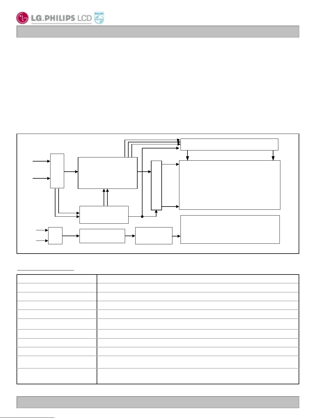
1. General Description
The LC230W01 is a Color Active Matrix Liquid Cr ystal Display with an integr al Cold Cathode Fluorescent
Lamp(CCFL) backlight system. The matrix employs a-Si Thin Film Transistor as the active element.
It is a transmissive type display operating in the normally black mode. This TFT-LCD has a 23.0 inch
diagonally measured active display area with WXGA resolution (768 vertic al by 1280 horizontal pixel arra y).
Each pixel is divided into Red, Green and Blue sub-pixels or dots which are arranged in vertical stripes.
Gray scale or the brightness of the sub-pixel color is determ ined with a 8-bit gray scale s ignal for each dot,
thus, presenting a palette of more than 16.7M(true) colors with 8Bit.
The LC230W01 has been designed to apply the 8Bit LVDS interface.
It is intended to support LCD TV, PCTV where high brightness, wide viewing angle, high color saturation,
and high color are important.
LVDS
5pair
+12.0V
+24.0V
GND
CN1
(20pin)
CN2
(12Pin)
General Features
RGB
Timing Controller
(LVDS Rx integrated)
Power Circuit
Block
Inverter
Block
23.01 inches(584.40mm) diagonalActive Screen Size
528.0(H) x 326.0(V) x 34.5(D) mm(Typ.)Outline Dimension
0.1305mm x 0.3915mm x RGBPixel Pitch
1280 horiz. By 768 vert. Pixels RGB strip arrangementPixel Format
16.7M colorsColor Depth
450 cd/m2 (Center 1 points typ.)Luminance, White
View Angle FreeViewing Angle(CR>10)
Total 67.8Watt (Typ.)Power Consumption
2,700g (Typ.)Weight
Gate Driver Circuit
2pin x 6CNs
(High)
Source Driver Circuit
S1 S1280
G1
TFT - LCD Panel
(1280 Ý RGB Ý 768 pixels)
G768
Back light Assembly
(Direct Light Type_12CCFL)
Transmissive mode, Normally BlackDisplay Operating Mode
Hard coating(3H), Anti-glare treatment of the front polarizer,Surface Treatment
Ver. 0.0 Apr. 02, 2003
4/ 29
Page 5
LC230W01
Liquid Crystal Display
Product Specification
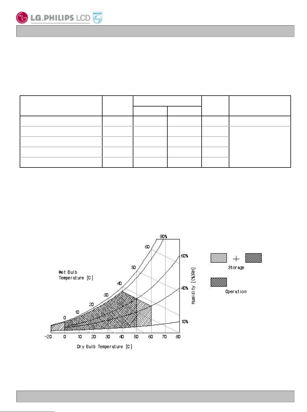
2. Absolute Maximum Ratings
The following are maximum values which, if exceeded, may cause faulty operation or damage to the unit.
Table 1. ABSOLUTE MAXIMUM RATINGS
Parameter Notes
Power Input Voltage
Operating Temperature
Storage Temperature
Operating Ambient Humidity
Storage Humidity
Symbol
LCD
Values
MaxMin
+500TOP
+60-20TST
Units
C
C
%RH9010HOP
%RH9010HST
Notes : 1. Temperature and relative humidity range are shown in the figure below.
Wet bulb temperature should be 39 C Max, and no condensation of water.
at 25 ± 5CVdc+14.0-0.3V
1
Ver. 0.0 Apr. 02, 2003
5/ 29
Page 6
LC230W01
Liquid Crystal Display
Product Specification
3. Electrical Specificati ons
3-1. Electrical Characteristics
The LC230W01 requires two power inputs. One is employed to power the LCD electronics and to drive the
TFT array and liquid crystal. The second input power for the CCFL/Backlight, is to power the inverter.
Table 2_1. LCD PANEL ELECTRICAL CHARACTERISTICS
Parameter Symbol
Values
Module :
Power Supply Input Voltage
Power Supply Input Current
Power Consumption
Rush current
LCD
I
LCD
LCD
RUSH
Notes: 1. The specified current and power consum ption are under the V
whereas mosaic pattern(8 x 6) is displayed and f
is the frame frequency.
V
2. The current is specified at the maximum current pattern.
3. The duration of rush current is about 2ms and rising time of Power Input is 1ms(min).
MaxTypMin
NotesUnit
Vdc12.612.011.4V
1mA270230-
mA 2360280-
Watt3.242.76P
1
3A2.0--I
=12.0V, 25C,fV=60Hz condition
LCD
Mosaic Pattern(8X6)
Ver. 0.0 Apr. 02, 2003
6/ 29
Page 7
Product Specification
Table 2_2. INVERTER ELECTRICAL CHARACTERISTICS
LC230W01
Liquid Crystal Display
Parameter Symbol
Values
NotesUnit
MaxTypMin
Inverter :
Power Supply Input Voltage
Power Supply Input Current
Power Consumption
DDB
DDB
B
Vdc25.224.022.8V
1A3.202.71-I
1W77.065.0-P
V3.30VBIBRTI Signal
V0.80VBPLLow
V5.02.0VBPHHigh
V5.02.0VBCH
V0.80VBSL
V5.02.0VBSH
Input Voltage for
Control System
Signals
BRTP
Signal
BRTC
Signal
PWSEL
Signal
Low V0.80VBCL
High
Low
High
Lamp :
Life Time
2Hrs50,000
Notes : 1. The specified current and power consumption are under the typical supply Input voltage, 24.0V.
2. The life is determined as the tim e at which luminance of the lamp is 50% compared to that of initial
value at the typical lamp current on condition of continuous operating at 25 ± 2C.
3. Electrical characteristics are determined after the unit has been ‘ON’ and stable for approximately
2Hrs in a dark environment at 25 C± 2C.
Ver. 0.0 Apr. 02, 2003
7/ 29
Page 8
LC230W01
Liquid Crystal Display
Product Specification
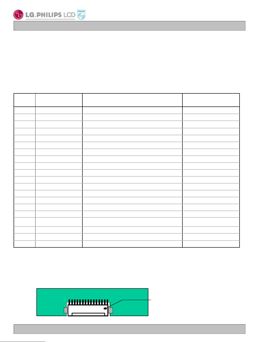
3-2. Interface Connections
This LCD employs Two interface connections, a 20 pin connector is used for the module electronics and a
12Pin Connector is used for the integral backlight system.
3-2-1. LCD Module
- LCD Connector DF14H-20P-1.25H(Manufactured by Hirose) or Equivalent
- Mating connector DF14-20S-1.25C(Manufactured by Hirose) or Equivalent
Table 3. MODULE CONNECTOR PIN CONFIGURATION
DescriptionSymbolPin No
V
LCD
2
LCD
Power Supply +12.0V1
Power Supply +12.0VV
Power Ground.GND3
Power GroundGND4
GroundGND7
GroundGND10
GroundGND13
GroundGND16
GroundGND19
GroundGND20
Output Pin #
(LVDS Tx)
PIN#48LVDS Receiver Signal(-)RXIN0-5
PIN#47LVDS Receiver Signal(+)RXIN0+6
PIN#46LVDS Receiver Signal(-)RXIN1-8
PIN#45LVDS Receiver Signal(+)RXIN1+9
PIN#42LVDS Receiver Signal(-)RXIN2-11
PIN#41LVDS Receiver Signal(+)RXIN2+12
PIN#40LVDS Receiver Clock Signal(-)RXCLK IN-14
PIN#39LVDS Receiver Clock Signal(+)RXCLK IN+15
PIN#38LVDS Receiver Signal(-)RXIN3-17
PIN#37LVDS Receiver Signal(+)RXIN3+18
Notes: 1. All GND(ground) pins s hould be connected together and to Vss which should also be connected
to the LCD’s metal frame.
2. All
V
(power input) pins should be connected together.
LCD
3. Input Level of LVDS signal is based on the IEA 664 Standard.
Rear view of LCM
1
20
DF14H-20P-1.25H(Hirose)
Ver. 0.0 Apr. 02, 2003
8/ 29
Page 9
LC230W01
Liquid Crystal Display
Product Specification
Table 4. REQUIRED SIGNAL ASSIGNMENT FOR FLATLINK’S Transmitter(THC63LVDM83A/LVDF83A)
OutputDescriptionSymbolPin NamePin #
51
52
54
55
56
2
Red Pixel DataRed0 [LSB]TxIN0
Red Pixel DataRed1TxIN1
Red Pixel DataRed2TxIN2
Red Pixel DataRed3TxIN3
Red Pixel DataRed4TxIN4
Red Pixel DataRed7 [MSB]TxIN5
Rx0-
Rx0+
Rx3-
Rx3+
10
11
12
14
15
16
18
19
20
22
23
24
25
27
28
30
50
3
4
6
7
8
RESTxIN23
TxIN24
TxIN25
TxIN26
TxIN27
Hsync.
Vsync.
EN
Red6
No connection, If unnecessary
No connection, If unnecessary
Red Pixel DataRed5TxIN6
Green Pixel DataGreen0 [LSB]TxIN7
Green Pixel DataGreen1TxIN8
Green Pixel DataGreen2TxIN9
Green Pixel DataGreen6TxIN10
Green Pixel DataGreen7 [MSB]TxIN11
Green Pixel DataGreen3TxIN12
Green Pixel DataGreen4TxIN13
Green Pixel DataGreen5TxIN14
Blue Pixel DataBlue0 [LSB]TxIN15
Blue Pixel DataBlue6TxIN16
Blue Pixel DataBlue7 [MSB]TxIN17
Blue Pixel DataBlue1TxIN18
Blue Pixel DataBlue2TxIN19
Blue Pixel DataBlue3TxIN20
Blue Pixel DataBlue4TxIN21
Blue Pixel DataBlue5TxIN22
Data Enable
Red Pixel Data
Rx0-
Rx0+
Rx1-
Rx1+
Rx3-
Rx3+
Rx1-
Rx1+
Rx3-
Rx3+
Rx1-
Rx1+
Rx2-
Rx2+
Rx3-
Rx3+
Rx2-
Rx2+
Rx3-
Rx3+
Notes: 1. Refer to LVDS Transmitter Data Sheet for detail descriptions.
2. 7 means MSB and 0 means LSB at R,G,B pixel data.
Ver. 0.0 Apr. 02, 2003
9/ 29
Page 10

Product Specification
LC230W01
Liquid Crystal Display
Table 5. REQUIRED SIGNAL ASSIGNMENT FOR LVDS Transmitter
Host System
24 Bit
RED0
RED1
RED2
RED3
RED4
RED5
RED6
RED7
GREEN0
GREEN1
GREEN2
GREEN3
GREEN4
GREEN5
GREEN6
GREEN7
BLUE0
BLUE1
BLUE2
BLUE3
BLUE4
BLUE5
BLUE6
BLUE7
Hsync
Vsync
Data Enable
CLOCK
THC63LVDM83A
or Compatible
51
52
54
55
56
3
50
2
4
6
7
11
12
14
8
10
15
19
20
22
23
24
16
18
27
28
30
31
TxOUT0TxOUT0+
TxOUT1TxOUT1+
TxOUT2TxOUT2+
TxCLKOUTTxCLKOUT+
TxOUT3TxOUT3+
DF14H-20P-1.25H
48
47
46
45
42
41
40
39
38
37
5
6
8
9
11
12
14
15
17
18
(THC63LVDM83A / LVDF83A)
Timing
Controller
100
100
100
100
100
RxIN0RxIN0+
RxIN1RxIN1+
RxIN2RxIN2+
RxCLKINRxCLKIN+
RxIN3RxIN3+
LCD Module
Notes : The LCD Module uses a 100Ohm r esistor between positive and negative lines of each receiver
input. Recommended Transmitter : See the data sheet for THC63LVDM83A(Thine Elec tronic s Inc.)
Ver. 0.0 Apr. 02, 2003
10 / 29
Page 11

Product Specification
3-2-2. Backlight Inverter
- Inverter Connector : S12B-PH-SM3-TB(Manufactured by JST) or Equivalent
- Mating Connector : PHR-12(Manufactured by JST) or Equivalent
Table 6. INVERTER CONNECTOR PIN CONFIGULATION
Power Supply +24.0VVDDB1
Power Supply +24.0VVDDB2
Power Supply +24.0VVDDB3
Not ConnectionNC4
Select of luminance control signal methodPWSEL5
PWM SignalBRTP6 Note 1
Luminance Control by voltage methodBRTI7
LC230W01
Liquid Crystal Display
RemarksDescriptionSymbolPin No
On : High or Open, Off : LowBacklight ON/OFF SignalBRTC8
Not ConnectionNC9
Backlight GroundGND10
Backlight GroundGND11 Note 2
Backlight GroundGND12
Notes : 1. See “3-7 Luminance controls”
2. GND is connected to the LCD’s metal frame.
Rear view of LCM
12
1
PCB
…
S12B-PH-SM3-TB
(JST : Japan Solderless Terminal Co.,Ltd.)
…
Ver. 0.0 Apr. 02, 2003
11 / 29
Page 12

LC230W01
Liquid Crystal Display
Product Specification
3-3. Signal Timing Specifications
This is the signal timing required at the input of the LVDS Transmitter. All of the interface signal tim ing s hould
be satisfied with the following specifications for it’s proper operation.
Table 7. TIMING TABLE
NoteUnitMaxTypMinSymbolITEM
DCLK
Hsync
Vsync
DE
(Data
Enable)
-12.512.2tCLKPeriod
MHz8280--Frequency
-16481328tHPPeriod
tCLK
kHz-48.5444.0fHFrequency
tCLK-168tWHWidth
tHP-810775tVPPeriod
636047fVFrequency
Hz
PAL : 47~53Hz
NTSC: 57~63Hz
tHP-62tWVWidth
128012801280tHVHorizontal Valid
-8016tHBPHorizontal Back Porch
tCLK
-27224tHFPHorizontal Front Porch
-36848-Horizontal Blank
768768768tVVVertical Valid
-203tVBPVertical Back Porch
tHP
-162tVFPVertical Front Porch
-427-Vertical Blank
Notes : Hsync period and Hsync width-active should be even number times of tCLK. If the value is odd number
times of t
CLK, display control signal can be asynchronous. In order to operate this LCM a Hsync.,
Vsync and DE(data enable) signals should be used.
1. The performance of the electro-optical characteristics are may be influenced by variance of the
vertical refresh rates.
2. Vsync, Hsync should be keep the above specification.
3. Hsync Period should be a double number of character (8).
Ver. 0.0 Apr. 02, 2003
12 / 29
Page 13

3-4. Signal Timing Waveforms
LC230W01
Liquid Crystal Display
Product Specification
DCLK
First data
Second data
DE(Data Enable)
Hsync, Vsync, DE, Data
tCLK
0.5 Vcc
Invalid data
Invalid data
Pixel 0,0
Pixel 1,0
0.7Vcc
Valid data
Pixel 2,0
Valid data
Pixel 3,0
0.3Vcc
Invalid data
Invalid data
tHP
HSync
t
WH
tHBP tHV
DE(Data Enable)
tVP
tWV
VSync
tVBP
DE(Data Enable)
Ver. 0.0 Apr. 02, 2003
tHFP
tVV tVFP
13 / 29
Page 14

LC230W01
Liquid Crystal Display
Product Specification
3-5. Color Input Data Reference
The Brightness of each primar y color(red,green,blue) is based on the 8-bit gray scale data input for the color;
the higher the binary input, the brighter the color. T he table below provides a reference for color versus data
input.
Table 8. COLOR DATA REFERENCE
Input Color Data
Basic
Color
RED
Color
Black 0 0 0 0 0 0 0 00 0 0 0 0 0 0 00 0 0 0 0 0 0 0
Red (255)
Green (255)
Blue (255)
Cyan
Magenta
Yellow
White
MSB LSB
RED
GREEN
MSB LSB
BLUE
MSB LSB
B7 B6 B5 B4 B3 B2 B1 B0G7 G6 G5 G4 G3 G2 G1 G0R7 R6 R5 R4 R3 R2 R1 R0
0 0 0 0 0 0 0 00 0 0 0 0 0 0 01 1 1 1 1 1 1 1
0 0 0 0 0 0 0 01 1 1 1 1 1 1 10 0 0 0 0 0 0 0
1 1 1 1 1 1 1 10 0 0 0 0 0 0 00 0 0 0 0 0 0 0
1 1 1 1 1 1 1 11 1 1 1 1 1 1 10 0 0 0 0 0 0 0
1 1 1 1 1 1 1 10 0 0 0 0 0 0 01 1 1 1 1 1 1 1
0 0 0 0 0 0 0 01 1 1 1 1 1 1 11 1 1 1 1 1 1 1
1 1 1 1 1 1 1 11 1 1 1 1 1 1 11 1 1 1 1 1 1 1
0 0 0 0 0 0 0 00 0 0 0 0 0 0 00 0 0 0 0 0 0 0RED (000) Dark
0 0 0 0 0 0 0 00 0 0 0 0 0 0 00 0 0 0 0 0 0 1RED (001)
............
0 0 0 0 0 0 0 00 0 0 0 0 0 0 01 1 1 1 1 1 1 0RED (254)
0 0 0 0 0 0 0 00 0 0 0 0 0 0 01 1 1 1 1 1 1 1RED (255)
0 0 0 0 0 0 0 00 0 0 0 0 0 0 00 0 0 0 0 0 0 0GREEN (000) Dark
GREEN
BLUE (000) Dark
BLUE
Ver. 0.0 Apr. 02, 2003
0 0 0 0 0 0 0 00 0 0 0 0 0 0 10 0 0 0 0 0 0 0GREEN (001)
............
0 0 0 0 0 0 0 01 1 1 1 1 1 1 00 0 0 0 0 0 0 0GREEN (254)
0 0 0 0 0 0 0 01 1 1 1 1 1 1 10 0 0 0 0 0 0 0GREEN (255)
0 0 0 0 0 0 0 00 0 0 0 0 0 0 00 0 0 0 0 0 0 0
0 0 0 0 0 0 0 10 0 0 0 0 0 0 00 0 0 0 0 0 0 0BLUE (001)
............
1 1 1 1 1 1 1 00 0 0 0 0 0 0 00 0 0 0 0 0 0 0BLUE (254)
1 1 1 1 1 1 1 10 0 0 0 0 0 0 00 0 0 0 0 0 0 0BLUE (255)
14 / 29
Page 15

3-6. Power Sequence
Power Supply For LCD
V
& Inverter V
LCD
DDB
0V
Product Specification
90% 90%
10%
T
1 T2 T5 T6 T7
LC230W01
Liquid Crystal Display
10%
Interface Signal
Power for LAMP(BRTC)
Table 9. POWER SEQUENCE
Parameter
10% 10%
Valid Data
T3 T4
Lamp ON
Values
MaxTypMin
--200T4
Units
ms10-1T1
ms50-0.5T2
ms--200T3
ms
ms50-0.5T5
ms10--T6
s--1T7
Notes : 1. Please avoid floating state of interface signal at invalid period.
2. When the interface signal is invalid, be sure to pull down the power supply for LCD V
3. Lamp power must be turn on after power supply for LCD an interface signal are valid.
Ver. 0.0 Apr. 02, 2003
DD
to 0V.
15 / 29
Page 16

3-7. LUMINANCE CONTROLS
3.7.1 Luminance Control Method
LC230W01
Liquid Crystal Display
Product Specification
Voltage Control
Pulse Width
Modulation
- Adjustment
This Control method can carry out continuation
adjustment of luminance, If it is adjusted within
the rated voltage for BRTI signal(VBI).
- Luminance ratio(these data are the target values)
Luminance ratioBRTI Voltage(VBI)
20%(Minimum)0V
100%(Maximum)3.3V
- Adjustment
Pulse Width Modulation(PWM) method works, when
PWSEL signal is Low and PWM signal(BRTP Signal)
is inputted into BRTP terminal. The luminance is con
-trolled by duty ratio of BRTP signal.
- Luminance ratio(these data are the target values)
Luminance ratioDuty ratio
20%(Minimum)0.2
100%(Maximum)1.0
High or Open
BRTP Signal
Open
PWM Signal
NotesPWSEL SignalAdjustment and Luminance RatioMethod
1Low
Notes : 1. See “3.7.2 Detail of PWM timing
2. The interference noise of luminance control frequency may appear on a display when investigating the
matching characteristics. If display noises appear on the display image, the discussion with LPL should
be done prior to implementation.
Ver. 0.0 Apr. 02, 2003
16 / 29
Page 17

3.7.2 Detail of PWM Timing
- Outline chart
BRTC
BRTP
- Detail of A part
VBPH
LC230W01
Liquid Crystal Display
Product Specification
A
0tPWL50ms 0tPWL50ms
0tPWL50ms
VBPL
tPWH tPWL
Notes : 1. Definition of parameters is as follows
FL= , DL=
1
tPW
2. See the following formula for luminance control frequency.
Luminance control frequency = tvv X (n+0.25)[or(n+0.72)]
n=1,2,3,…………
tvv : See “3.3 Signal timing specification”
The interference noise of luminance control frequency and input signal frequency for LCD
panel signal processing board may appear on a display. Set up luminance control frequency
so that the interference noise does not appear.
3. See “3.7.1 Luminance control methods”
4. If tPWL is more than 50ms, the backlight will be turned off by a protection circuit for inverter.
tPW
NotesUnitMax.Typ.Min.SymbolParameter
1, 2Hz280255230FLLuminance control frequency
1, 3-1.0-0.2DLDuty Ratio
4Ms50-0tPWLNon signal Period
tPWH
tPW
Ver. 0.0 Apr. 02, 2003
17 / 29
Page 18

LC230W01
Liquid Crystal Display
Product Specification
4. Optical Specification
Optical characteristics are determined after the unit has been ‘ON’ and stable for approximatel y 2Hrs in a dar k
environment at 25·2¶C. The values specified are at an approximate distance 50cm fr om the LCD surf ace
at a viewing angle of Φ and θ equal to 0 ¶.
FIG. 1 presents additional information concerning the measurement equipment and method.
FIG. 1 Optical Characteristic Measurement Equipment and Method
Optical Stage(x,y)
LCD Module
Table 10. OPTICAL CHARACTERISTICS
Parameter Symbol NotesUnits
Surface Luminance, white
Luminance Variation
Response
Time
Color Coordinates
Viewing Angle (CR>10)
Rise Time
Decay Time
RED
GREEN
BLUE
x axis, right(φ=0) 5degree-8885θr
x axis, left (φ=180)
y axis, up (φ=90)
y axis, down (φ=270)
WH
WHITE
RX
RY
GX
GY
BX
BY
WXWHITE
WY
500mm
5P
Typ –0.03
Values
Pritchard 880 or
equivalent
Ta:252 C, V
MaxTypMin
-450300L
3015TrR
2010TrD
Typ +0.03
-8885θl
-8885θu
-8885θd
:12.0V, fV:60Hz,
LCD
Dclk:80MHz, ILamp=6mA
1-400280CRContrast Ratio
2
2cd/m
31.3-δ
4ms
62.2Gray Scale
Ver. 0.0 Apr. 02, 2003
18 / 29
Page 19

Product Specification
Notes : 1. Contrast Ratio(CR) is defined mathematically as :
Surface Luminance with all white pixels
Contrast Ratio =
Surface Luminance with all black pixels
Surface luminance is the center point(1).
2. Surface luminance is the center point(1) across the LCD surface 50cm from the surface with all
pixels displaying white under the condition of I
BL=6mArms. For more information see FIG 1.
LC230W01
Liquid Crystal Display
3. The variation in surface luminance , δ W HITE is defined by measuring L
position 1 through 5, and then dividing maximum L
ON of 5 points luminance b y minimum LON of
ON at watch test
each 5points luminance. For more information see FIG 2.
δ WHITE = Maximum (L
ON1, LON2, ........, LON5 ) / Minimum (LON1, LON2, ........, LON5 )
4. Response time is the time required f or the display to trans ition from black to white (Ris e Tim e,
T
rR) and from white to black (Decay Time, TrD). For additional information see FIG 3.
5. Viewing angle is the angle at which the contrast ratio is greater than 10. The angles are
determined for the horizontal or x axis and the vertical or y axis with respect to the z axis which
is normal to the LCD surface. For more information see FIG 4.
6. Gray scale specification
Gray Level
L0
L15
L31
L47
L63
L79
L95
L111
L127
L143
L159
L175
L191
L207
L223
L239
L255
Luminance [%] (Typ)
TYP
0.3
0.65
1.2
2.5
4.68
7.8
11.7
16.0
21.2
27.7
35.2
43.5
53.0
63.7
75.4
86.4
100
Ver. 0.0 Apr. 02, 2003
19 / 29
Page 20

Product Specification
FIG. 2 Luminance
<measuring point for surface luminance & measuring point for luminance variation>
H
A
LC230W01
Liquid Crystal Display
L2
L3
B
V
L1
A : H/4 mm,
B : V/4 mm,
L5L4
H : 501.12 mm
V : 300.67 mm
@ H,V : Active Area
Active Area
FIG. 3 Response Time
The response time is defined as the following figure and shall be measured by switching the input signal
for “black” and “white”.
TrR
TrD
100
90
Optical
Response
10
0
Ver. 0.0 Apr. 02, 2003
20 / 29
Page 21

FIG. 4 Viewing angle
φ
= 180°, Left
Product Specification
<Dimension of viewing angle range>
Normal
E
θ
φ
Y
φ
= 90°, Up
LC230W01
Liquid Crystal Display
φ
= 270°, Down
φ
= 0°, Right
Ver. 0.0 Apr. 02, 2003
21 / 29
Page 22

LC230W01
Liquid Crystal Display
Product Specification
5. Mechanical Characteristics
The contents provide general mechanical characteristics for the model LC230W01. In addition the figures
in the next page are detailed mechanical drawing of the LCD.
528.0mmHorizontal
Outline Dimension
Bezel Area
Active Disp lay Area
2,700g (Typ.) , 2,800g (Max.)Weight
Surface Treatment
Hard coating(3H)
Anti-glare treatment of the front polarizer
Note : See Attached Drawing(Front / Rear View)
326.0mmVertical
34.5mmDepth
506.0mmHorizontal
305.6mmVertical
501.12mmHorizontal
300.67mmVertical
Ver. 0.0 Apr. 02, 2003
22 / 29
Page 23

<FRONT VIEW>
LC230W01
Liquid Crystal Display
Product Specification
Ver. 0.0 Apr. 02, 2003
23 / 29
Page 24

<REAR VIEW>
LC230W01
Liquid Crystal Display
Product Specification
Ver. 0.0 Apr. 02, 2003
24 / 29
Page 25

6. Reliability
Environment test condition
No Test Item Condition
LC230W01
Liquid Crystal Display
Product Specification
1
2
3
4
Ta= 60¶C 240hHigh temperature storage test
Ta= -20¶C 240hLow temperature storage test
Ta= 50¶C 50%RH 240hHigh temperature operation test
Ta= 0¶C 240hLow temperature operation test
Wave form : random
5
Vibration test
(non-operating)
Vibration level : 1.0Grms
Bandwidth : 10-500Hz
Duration : X,Y,Z, 10 min
One time each direction
Shock level : 100Grms
6
Shock test
(non-operating)
Waveform : half sine wave, 2ms
Direction : X, Y, Z
One time each direction
Humidity condition Operation7
Altitude
8
operating
storage / shipment
Ta= 40 ¶C ,90%RH
0 - 14,000 feet(4267.2m)
0 - 40,000 feet(12192m)
Ver. 0.0 Apr. 02, 2003
25 / 29
Page 26

LC230W01
Liquid Crystal Display
Product Specification
7. International Standards
7-1. Safety
a) UL 1950 Third Edition, Underwriters Laboratories, Inc. Jan. 28, 1995.
Standard for Safety of Information Technology Equipment Including Electrical Business Equipment.
b) CAN/CSA C22.2 No. 950-95 Third Edition, Canadian Standards Association, Jan. 28, 1995.
Standard for Safety of Information Technology Equipment Including Electrical Business Equipment.
c) EN 60950 : 1992+A1: 1993+A2: 1993+A3: 1995+A4: 1997+A11: 1997
IEC 950 : 1991+A1: 1992+A2: 1993+A3: 1995+A4: 1996
European Committee for Electrotechnical Standardization(CENELEC)
EUROPEAN STANDARD for Saf ety of Information T echnology Equipment Including Electrical Bus iness
Equipment.
7-2. EMC
a) ANSI C63.4 “Methods of Measurement of Radio-Noise Emissions from Low-Voltage Electrical and
Electrical Equipment in the Range of 9kHZ to 40GHz. “American National Standards Institute(ANSI),
1992
b) C.I.S.P.R “Limits and Methods of Measurement of Radio Interface Characteristics of Information
Technology Equipment.“ International Special Committee on Radio Interference.
c) EN 55022 “Limits and Methods of Measurement of Radio Interface Characteristics of Information
Technology Equipment.“ European Committee for Electrotechnical Standardization.(CENELEC), 1998
Ver. 0.0 Apr. 02, 2003
26 / 29
Page 27

8. Packing
8-1. Designation of Lot Mark
a) Lot Mark
ABCDEFGHI JKLM
A,B,C : SIZE
D : YEAR
E : MONTH
F,G : PANEL CODE
H : ASSEMBLY CODE
I,J,K,L,M : SERIAL NO.
Note
1. YEAR
LC230W01
Liquid Crystal Display
Product Specification
Year
Mark
200012001
0
2002320034200452005
2
2. MONTH
Month
Mark
Apr5May
4
Jun7Jul8Aug9Sep
6
3. Serial No.
100000 ~1 ~ 99999Year
A0001 ~ A9999, ..... , Z999900001 ~ 99999Mark
b) Location of Lot Mark
Serial NO. is printed on the label. The label is attached to the backside of the LCD module.
This is subject to change without prior notice.
8-2. Packing Form
a) Package quantity in one box : 3 pcs
2006
6
Oct
A
2007999897
Nov
7987
DecMarFebJan
B
C421
b) Box Size : 488mm X 245mm X 657mm
Ver. 0.0 Apr. 02, 2003
27 / 29
Page 28

LC230W01
Liquid Crystal Display
Product Specification
9. PRECAUTIONS
Please pay attention to the followings when you use this TFT LCD module.
9-1. MOUNTING PRECAUTIONS
(1) You must mount a module using holes arranged in four corners or four sides.
(2) You should consider the mounting structure so that uneven force (ex. Twisted stress) is not applied to the
module. And the case on which a module is m ounted should have sufficient str ength so that external
force is not transmitted directly to the module.
(3) Please attach the surface transparent protective plate to the surface in order to protect the polarizer.
Transparent protective plate should have sufficient strength in order to the resist external force.
(4) You should adopt radiation structure to satisfy the temperature specification.
(5) Acetic acid type and chlorine t ype materials for the cover case are not desirable because the former
generates corrosive gas of attacking the polarizer at high temperature and the latter causes circuit break
by electro-chemical reaction.
(6) Do not touch, push or rub the exposed polarizers with glass, tweezers or anything harder than HB
pencil lead. And please do not rub with dust clothes with chemical treatment.
Do not touch the surface of polarizer for bare hand or greasy cloth.(Some cosmetics are detrimental
to the polarizer.)
(7) When the surface becomes dusty, please wipe gently with absorbent cotton or other s oft materials like
chamois soaks with petroleum benzene. Normal-hexane is recommended for cleaning the adhesives
used to attach front / rear polarizers. Do not use acetone, toluene and alcohol because they cause
chemical damage to the polarizer.
(8) Wipe off saliva or water drops as soon as possible. Their long time contact with polarizer causes
deformations and color fading.
(9) Do not open the case because inside circuits do not have sufficient strength.
9-2. OPERATING PRECAUTIONS
(1) The spike noise causes the mis-operation of circuits. It should be lower than following voltage :
V=·200mV(Over and under shoot voltage)
(2) Response time depends on the temperature.(In lower temperature, it becomes longer.)
(3) Brightness depends on the temperature. (In lower temperature, it becomes lower.)
And in lower temperature, response time(required time that brightness is stable after turned on) becomes
longer.
(4) Be careful for condensation at sudden temperature change. Condensation makes damage to polarizer or
electrical contacted parts. And after fading condensation, smear or spot will occur.
(5) When fixed patterns are displayed for a long time, remnant image is likely to occur.
(6) Module has high frequency circuits. Sufficient suppression to the electromagnetic interference shall be
done by system manufacturers. Grounding and shielding methods may be important to minimized the
interference.
(7) Please do not give any mechanical and/or acoustical impact to LCM. Otherwise, LCM can not be operated
its full characteristics perfectly.
(8) A screw which is fastened up the steels should be a machine screw (if not, it causes metal foreign
material and deal LCM a fatal blow)
Ver. 0.0 Apr. 02, 2003
28 / 29
Page 29

LC230W01
Liquid Crystal Display
Product Specification
9-3. ELECTROSTATIC DISCHARGE CONTROL
Since a module is composed of electronic circ uits, it is not str ong to electrostatic dis charge. Mak e certain that
treatment persons are connected to ground through wrist band etc. And don’t touch interface pin directly.
9-4. PRECAUTIONS FOR STRONG LIGHT EXPOSURE
Strong light exposure causes degradation of polarizer and color filter.
9-5. STORAGE
When storing modules as spares for a long time, the following precautions are necessary.
(1) Store them in a dark place. Do not expose the module to sunlight or fluorescent light. Keep the
temperature between 5¶C and 35¶C at normal humidity.
(2) The polarizer surface should not come in contact with any other object.
It is recommended that they be stored in the container in which they were shipped.
9-6. HANDLING PRECAUTIONS FOR PROTECTION FILM
(1) The protection film is attached to the bezel with a small masking tape.
When the protection film is peeled off, static electricity is generated between the film and polarizer.
This should be peeled off slowly and caref ully by people who are electrically grounded and with well
ion-blown equipment or in such a condition, etc.
(2) When the module with pr otection film attached is stored for a long time, sometimes there remains a
very small amount of glue still on the bezel after the protection film is peeled off.
(3) You can remove the glue easily. When the glue remains on the bezel surface or its vestige is recognized,
please wipe them off with absorbent cotton waste or other soft material like chamois soaked with normal
-hexane.
Ver. 0.0 Apr. 02, 2003
29 / 29
 Loading...