

LG Innotek BH1000 User Manual

User Guide for the LTD-BH1000
Product: WCDMA Wireless Modem
Model name: LTD-BH1000
Table of Contents
1. Overview
2. Major features
3. Interface
4. Electrical specifications
5. RF specifications
6. Mechanical specifications
7. General specifications
8. Connectors
9. RFx information
10. FCC approval
Copyright ⓒ. 2014. All Rights Reserved.

1. Overview
The LTD-BH1000 is a personal mobile communication device that incorporates
the latest compact radio technology, including smaller and lighter components
and support for WCDMA(850/1900MHz) bands. This device acts as the
vehicle’s telematics system and connects to WCDMA (HSPA+) wireless
networks and wireless modules to allow voice and data communication.
Furthermore, this device can operate on land and water as well as other similar
areas.
In HSPA+ mode, the device provides uplink speeds of up to 5.76 Mbps and
downlink speeds of up to 14.4 Mbps for seamless transfer of data such as
movies and video calls. The device also supports the transfer of large amounts
of data.
The device communicates with the host system via a standard RS-232 or USB
port, and AT commands and control commands can be used to send data. Voice
calls are also possible.
Copyright ⓒ. 2014. All Rights Reserved.

93.7(L) x 42(W) x 7.6(T) mm
Technology
2. Major features
Mechanical
Dimensions
Weight
Interface
Antenna
Temperature*
Main chipset
Memory
TBD g (max)
USB, general purpose I/O pins
FAKRA connector
Operation: -20 ℃ - +70 ℃
Storage: -40 ℃ - +85 ℃
MDM 6200
1024Mb(NAND) / 512Mb(SDRAM)
ETC
Standard
Band
Power
DC power
Functions
3GPP WCDMA (HSPA+)
- DL Speed : 14.4 Mbps
- UL Speed : 5.76 Mbps
WCDMA B2, B5
WCDMA : Typ. 24dBm (Power Class 3)
4 V
Voice, data, SMS
Copyright ⓒ. 2014. All Rights Reserved.
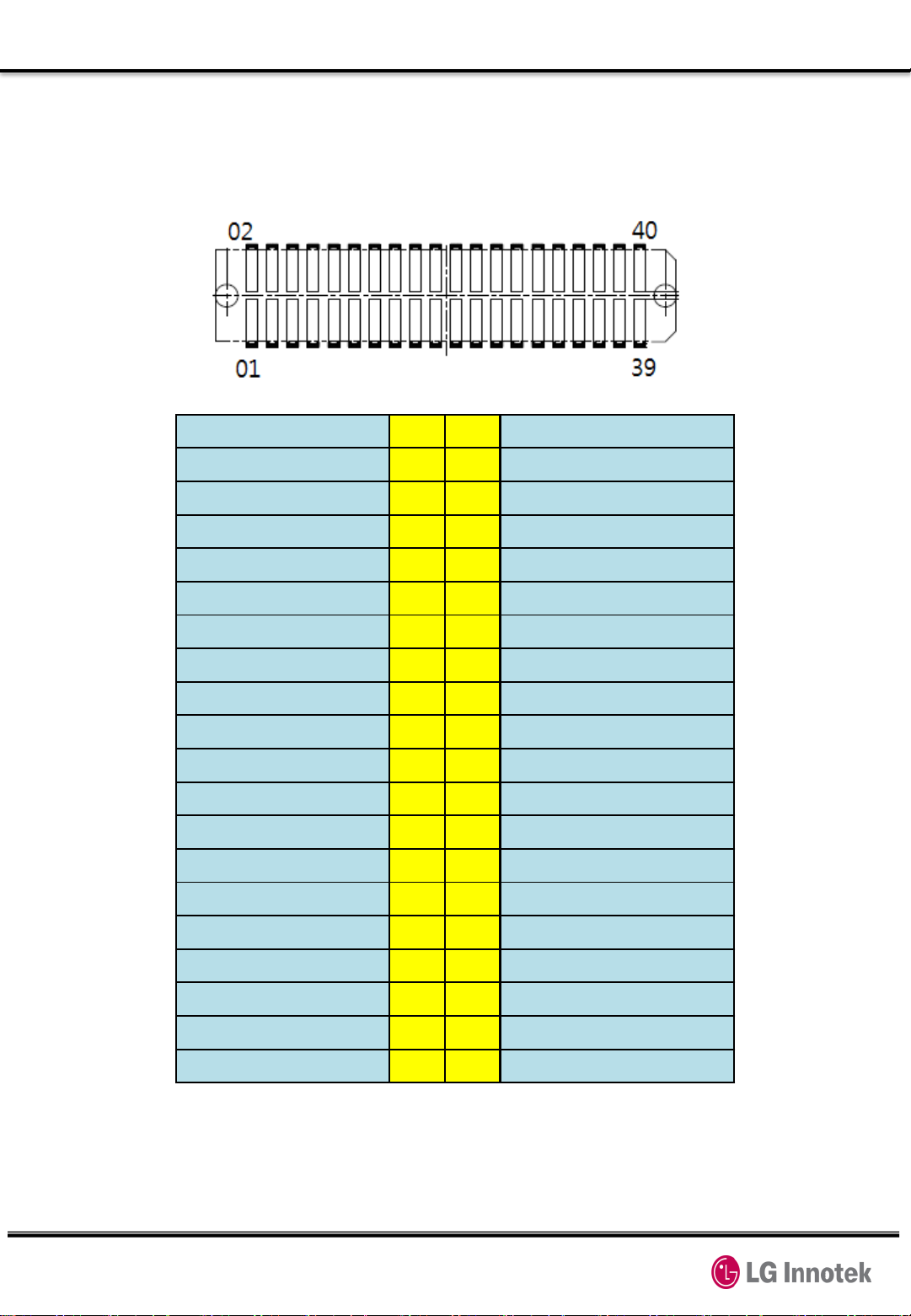
3. Interface
NC 1 2 NC
GND 3 4 GND
NC 5 6 NC
NC 7 8 NC
NC 9 10 NC
BOOT_OK 11 12 MSG
NC 13 14 NC
NC 15 16 PCM_3.3V_TXD
GND 17 18 PCM_3.3V_RXD
PCM_3.3V_CLK 19 20 PCM_3.3V_SYNC
GND 21 22 GND
NC 23 24 NC
NC 25 26 NC
96H_END 27 28 RESET_IN
USB_VBUS 29 30 ACC_ON_SLEEP
V_BATT 31 32 V_BATT
GND 33 34 GND
GND 35 36 USB_D-
UART_RXD 37 38 USB_D+
UART_TXD 39 40 GND
3.1 Pin output
Customer P/N is connected with outer device using 40 pin connector
Copyright ⓒ. 2014. All Rights Reserved.
Figure 1. Connector pin arrangement

3. Interface
USB_D
USB_D
USB_VBUS
USB
USB
USB
PCM_3.3V_SYNC
PCM_3.3V_CLK
PCM_3.3V_TXD
PCM_3.3V_RXD
PCM
PCM
PCM interface digital audio data out
PCM
BOOT_
RESET_IN
MSG
96H_END
ACC
Indicates that the Modem boot is complete.
Control line to unconditionally restart the module.
Indicates
Urgent message.
Indicates
Control line to power on or 96hr
VBATT
GND
3,4,17,21,22,33
Power supply
Power supply
UART_RXD
UART_TXD
UART RX
UART TX DATA
RESERVED
1,2,5,6,7,8,9,10
,13,14,15,23,24
Reserved pins. Please leave
3.2 Pin description
Signal Name
Type
Pin
Description
USB
Audio
PCM
User
Interface
Power
+
-
OK
_ON_SLEEP
IO
IO
I
I
I
O
I
O
I
O
O
I
I
-
38
36
29
20
19
16
18
11
28
12
27
30
31,32
,35,40
differential data line (+)
differential data line (-)
power Supply
interface sync
interface clock
interface digital audio data in
that the Modem receive
that the 96hr sleep mode is end.
input (+)
input (-)
sleep mode.
UART
NC
Copyright ⓒ. 2014. All Rights Reserved.
I
O
-
Table 1. Pin descriptions
37
39
,25,26
DATA
these unconnected

3. Interface
3.3 USB
This device supports universal serial bus (USB) connections for high-speed
data communication. The relevant hardware satisfies the USB 2.0
specifications and supports maximum communications speeds of 480 Mbps
Pin NO. Signal Name
38
36
29
USB_D+
USB_D-
USB_VBUS
Pin I/O
(Modem host)
IO
IO
I
Function Description
USB Differential data line (+)
USB Differential data line (-)
Table 2. USB Pin descriptions
USB Power Supply
Copyright ⓒ. 2014. All Rights Reserved.

3. Interface
3.4 Audio
This module includes a PCM interface. The pull-up and pull-down resistors
attached to these pin must provide more than 50 Kohm of resistance.
Pin NO.
20 PCM_3.3V_SYNC
19 PCM_3.3V_CLK
16 PCM_3.3V_TXD
18
PCM_3.3V_RXD
Signal Name
3.5 User interface
Pin No.
Signal Name Direction
Pin I/O
(Modem host)
I
I
O
I
PCM Interface sync
PCM Interface clock
PCM Interface digital audio data out
PCM Interface digital audio data in
Table 3. PCM Pin descriptions
Function Description
Function
11
BOOT_OK
O
28 RESET_IN I
12 MSG O
27 96H_END O
30 ACC_ON_SLEEP
I
Table 4. User interface Pin descriptions
Indicates that the Modem boot is complete.
Control line to unconditionally restart the
module.
Indicates that the Modem receive Urgent
message.
Indicates that the 96hr sleep mode is end.
Control line to power on or 96hr sleep mode.
Copyright ⓒ. 2014. All Rights Reserved.

4. Electrical specifications
4.1 Power supply specifications
The host system provides the power supply (V_BATT)DC 4 V, 1.5 A to the
device. The internal power supply module manages the power supplied to the
integral circuits and maintains constant voltages. This module also controls
each power block to minimize power consumption.
In particular, the PAM (power amplifier module) consumes a lot of power, so it
receives a direct power supply of 4 V from the V_BATT. Therefore the
V_BATT signal inputs only the supply power of the PAM, even when the
absolute rating is higher. In addition, the entire power input module blocks and
protects against high surges and ESD in the NAD module.
Pin No. Signal Name Direction MIN TYP MAX
31,32 V_BATT I TBD V 4 V TBD V
Table 5. Power supply specifications
Copyright ⓒ. 2014. All Rights Reserved.

4. Electrical specifications
ACC_ON_SLEEP
4.2 Logic level specifications
4.2.1 Digital logic level specifications
Signal Name Type
BOOT_OK O -0.3 0.63 1.17 2.1
RESET_IN I 0 0.45 1.35 1.8
MSG O -0.3 0.63 1.17 2.1
96H_END O -0.3 0.63 1.17 2.1
I 0 0.45 1.35 1.8
Low High
Min Max Min Max
Table 6. Digital logic level specifications
Unit
V
Copyright ⓒ. 2014. All Rights Reserved.
5. RF specifications
20.51dBm ~ 25.5dBm
5.1 WCDMA
5.1.1 Receiver
.- Bandwidth : 5MHz
.- Frequency : 869MHz – 894MHz (B5), 1930MHz – 1990MHz (B2)
.- RF to Baseband Direct conversion (Zero IF)
.- Modulation method : QPSK, 16QAM
.- Sensitivity : ≤-104dBm (BER = Under 0.1%)
5.1.2 Transmitter
.- Frequency: 824MHz – 849MHz (B5), 1850MHz – 1910MHz (B2)
.- Maximum RF Output : Power class3 , 20.3dBm ~ 25.7dBm
.- Modulation method : QPSK
.- Baseband to RF Direct conversion (Zero IF)
Copyright ⓒ. 2014. All Rights Reserved.

6. Mechanical specifications
6.1 Environment specifications
.- Storage temp.: -40 ℃ - +85 ℃
.- Operating temp.: -20 ℃ - +70 ℃
(-20 ℃ - +70 ℃ : 3GPP specifications are satisfied
-30 ℃ - -20 ℃, +70 ℃ - +80 ℃ : May cause performance degradation)
.- Operating humidity: 80% (60℃) relative humidity
Copyright ⓒ. 2014. All Rights Reserved.
 Loading...