

Page 1
()Preliminary Specification
(●) Final Specification
Title 17.3” FHD TFT LCD
LP173WF3
Liquid Crystal Display
Product Specification
SPECIFICATION
FOR
APPROVAL
BUYER
MODEL
APPROVED BY SIGNATURE
/
/
/
SUPPLIER LG Display Co., Ltd.
*MODEL LP173WF3
Suffix SLB3
*When you obtain standard approval,
please use the above model name without suffix
APPROVED BY
S. R. Kim / S.Manager
REVIEWED BY
M. J. Lee / S.Manager
PREPARED BY
S. I. Joo / Engineer
J. P. Lee / Engineer
SIGNATURE
Please return 1 copy for your confirmation with
your signature and comments.
Ver. 1.1
Ver. 1.1
20. Oct. 2011
20. Oct. 2011
Products Engineering Dept.
LG Display Co., Ltd
1/ 34
Page 2
Product Specification
Contents
LP173WF3
Liquid Crystal Display
No ITEM
COVER
CONTENTS
RECORD OF REVISIONS
1 GENERAL DESCRIPTION
2 ABSOLUTE MAXIMUM RATINGS
3 ELECTRICAL SPECIFICATIONS
3-1 ELECTRICAL CHARACTREISTICS
3-2 INTERFACE CONNECTIONS
3-3 LVDS SIGNAL TIMING SPECIFICATIONS
3-4 SIGNAL TIMING SPECIFICATIONS
3-5 SIGNAL TIMING WAVEFORMS
3-6 COLOR INPUT DATA REFERNECE
3-7 POWER SEQUENCE
4 OPTICAL SFECIFICATIONS
Page
1
2
3
4
5
6
7
8
11
11
12
13
14
Ver. 1.1
Ver. 1.1
5 MECHANICAL CHARACTERISTICS
6 RELIABLITY
7 INTERNATIONAL STANDARDS
7-1 SAFETY
7-2 EMC
8 PACKING
8-1 DESIGNATION OF LOT MARK
8-2 PACKING FORM
9 PRECAUTIONS
A APPENDIX. Enhanced Extended Display Identification Data
20. Oct. 2011
20. Oct. 2011
18
27
28
28
29
29
30
32-34
2 / 34
Page 3
Product Specification
RECORD OF REVISIONS
LP173WF3
Liquid Crystal Display
Revision No Revision Date Page Description
1.0 17. Aug. 2011 - Final Specification 1.0
1.1 20. Oct. 2011 20 Update Rear View Drawing 1.0
EDID
ver
Ver. 1.1
Ver. 1.1
20. Oct. 2011
20. Oct. 2011
3 / 34
Page 4
LP173WF3
Liquid Crystal Display
Product Specification
1. General Description
The LP173WF3 is a Color Active Matrix Liquid Crys tal Disp lay with an integral RGB LED backligh t s ystem.
The matrix employs a-Si Thin Film Transistor as the active element. It is a transmissive type display
operating in the normally black mode. This TFT-LCD has 17.3 inches diagonally measured active display
area with Full HD resolution(1920 horizontal by 1080 vertical pixel ar ray). Each pixel is divided into Red,
Green and Blue sub-pixels or dots which are arranged in ver tica l s tripes . G ray scale or the br ightness o f the
sub-pixel color is determined with a 10-bit gray scale signal for each dot, thus, presenting a palette of more
than 1.073G(True) colors.
The LP173WF3 has been designed to apply the inte rface me thod that enables low power, high speed, low
EMI. The LP173WF3 is intended to support applications where thin thickness, low power are critical factors
and graphic displays are important. In combination with the vertical arrangement of the sub-pixels, the
LP173WF3(SLB3) characteris tics provide an excellent flat display for office automation products such as
Notebook PC.
17.3 TFT-LCD Pa n el
17.3 TFT-LCD Pa n el
General Features
Active Screen Size 17.3 inches diagonal
Outline Dimension 398.1 (H, Typ) × 234.3 (V, Typ) × 7.2(D, Max) mm
Pixel Pitch 0.199mm × 0.199 mm
Pixel Format 1920 horiz. by 1080 vert. Pixels RGB strip arrangement
Color Depth 10-bit, 1.073G colors
Luminance, White 300 cd/m2(Typ.), 5 point
Power Consumption 18.2W (Typ.) [4.10W (Logic, Typ.) + 14.1W (B/L, Typ.)]
Weight (Max.) 830g
Display Operating Mode Transmissive mode, Normally black
Surface Treatment Hard coating(3H), Anti-Glare treatment of the front polarizer
(1920 X 1080)
(1920 X 1080)
Ver. 1.1
Ver. 1.1
20. Oct. 2011
20. Oct. 2011
4 / 34
Page 5
LP173WF3
Liquid Crystal Display
Product Specification
2. Absolute Maximum Ratings
The following are maximum values which, if exceeded, may cause faulty operation or damage to the unit.
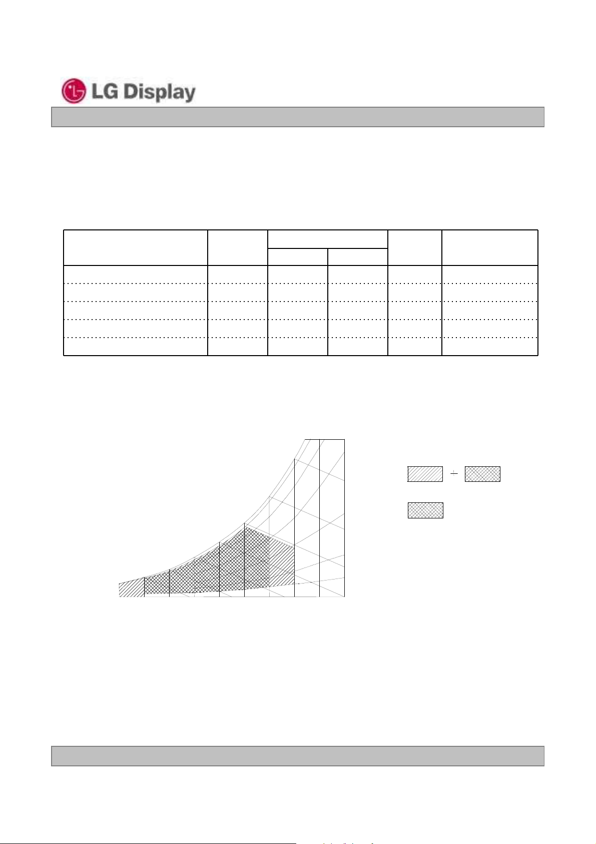
Table 1. ABSOLUTE MAXIMUM RATINGS
Parameter Symbol
Power Input Voltage
Operating Temperature
Storage Temperature
Operating Ambient Humidity
Storage Humidity
VCC -0.3 4.0 Vdc at 25 5C
TOP 050C1
HST -20 60 C1
HOP 10 90 %RH 1
HST 10 90 %RH 1
Values
Units Notes
Min Max
Note : 1. Temperature and relative humidity range are shown in the figure below.
Wet bulb temperature should be 39
C Max, and no condensation of water.
Note : 2. Storage Condition is guaranteed under packing condition.
90% 80%
60%
Humidity[(%)RH]
Storage
40%
Operation
20%
10%
Wet Bulb
Temperature [℃]
20
10
0
60
50
40
30
Ver. 1.1
Ver. 1.1
-20
10
20 30 40 50
Dry Bulb Temperature [℃]
20. Oct. 2011
20. Oct. 2011
60 70 800
5 / 34
Page 6
LP173WF3
Liquid Crystal Display
Product Specification
3. Electrical Specifications
3-1. Electrical Characteristics
The LP173WF3(SLB3)requires two power inputs. One is employed to power the LC D electronics and to
drive the TFT array and liquid crys tal. The second input which powers the LED, is typically genera ted by an
LED Driver. The LED Driver is an internal unit to the LCD.
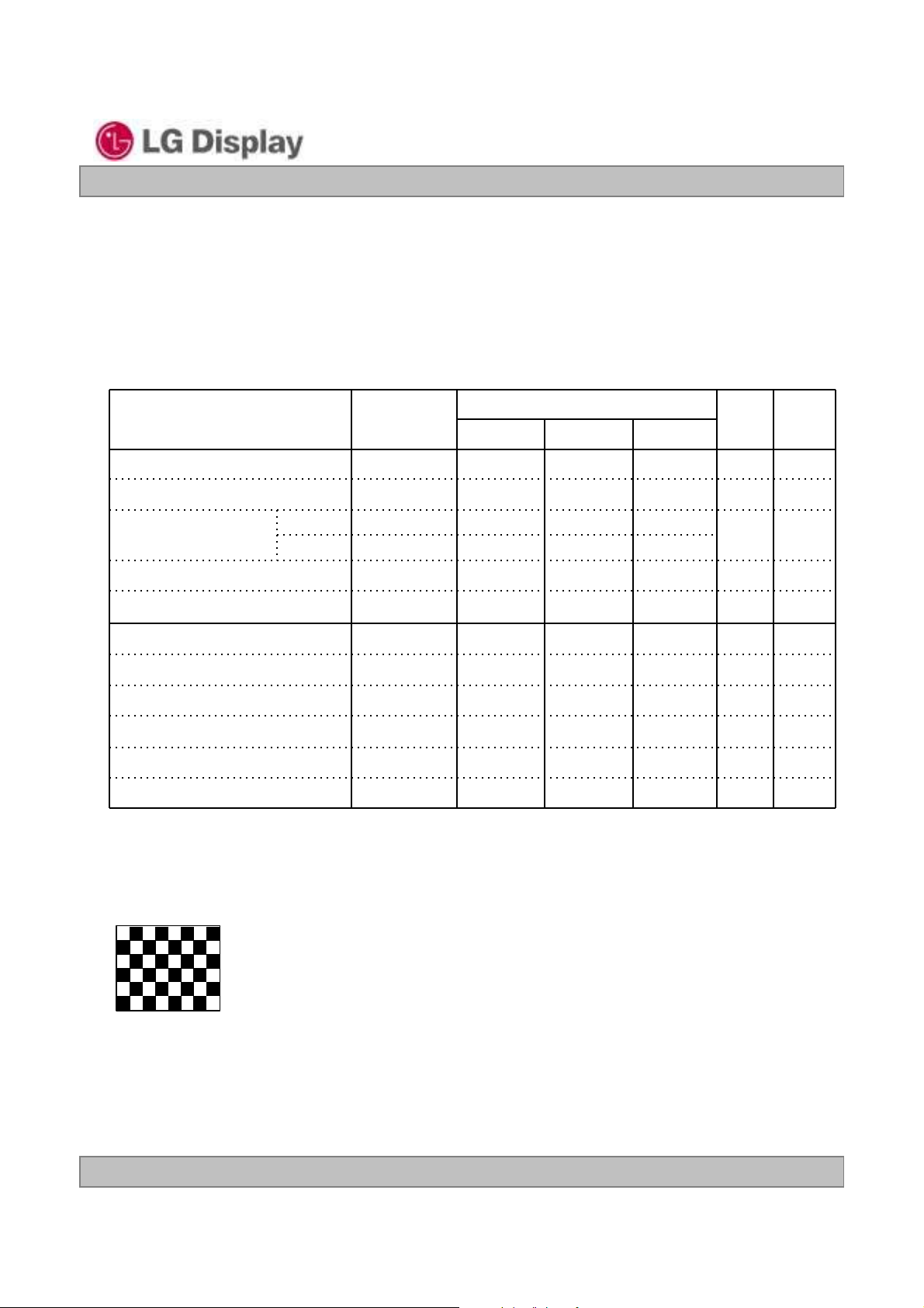
Table 2. ELECTRICAL CHARACTERISTICS
Parameter Symbol
MODULE :
Power Supply Input Voltage VCC 3.0 3.3 3.6 V
Power Supply Input
Current
Power Consumption (Mosaic) Pc - 4.1 4.92 Watt 1
Differential Impedance
LED Backlight :
Power Supply Input Voltage V
Operating Voltage V
Operating Current per string I
Power Consumption P
Life Time 15,000 - - Hrs 5
Mosaic I
White I
CC
CC
Zm
BL+
LED (R,G,B)
LED (R,G,B)
BL
Min Typ Max
1.03 1.24 1.49
1.29 1.52 1.75
90 100 110 Ohm 2
7.5 14.4 21 V
--45V3
--50mA3
Values
Unit Notes
DC
A1
DC
14.1 16.2 Watt 4
Note)
1. The specified current and power consumption are under the Vcc = 3.3V , 25℃, fv = 60Hz condition
whereas Mosaic pattern (8x6) is displayed and fv is the frame frequency.
2. This impedance value is needed to proper display and measured form LVDS Tx to the mating connector.
3. RGB LED
Operating Voltage and Operating Current per string should be within Max. SPEC.
4. The LED power consumption ( Typ ) shown above does include power of internal LED driver circuit
for typical current condition. ( Luminance = 300nit condition )
The power consumption ( Max ) condition is R,G,B LED 100% Dimming.
5. The life time is determined as the time at which brightness of LED is 50% compare to that of initial value
at the typical LED current.
Ver. 1.1
Ver. 1.1
20. Oct. 2011
20. Oct. 2011
6 / 34
Page 7
LP173WF3
Liquid Crystal Display
Product Specification
3-2. Interface Connections
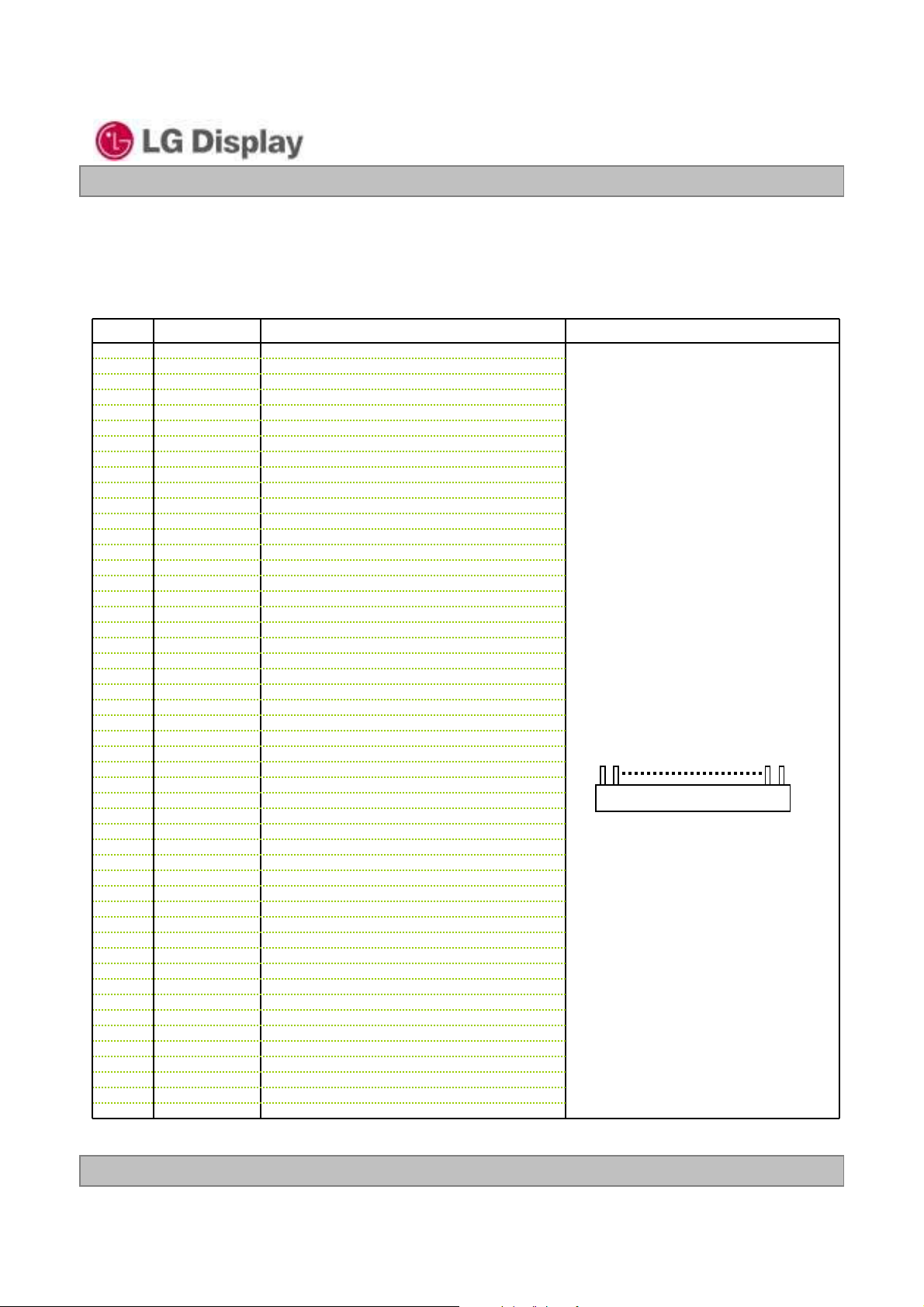
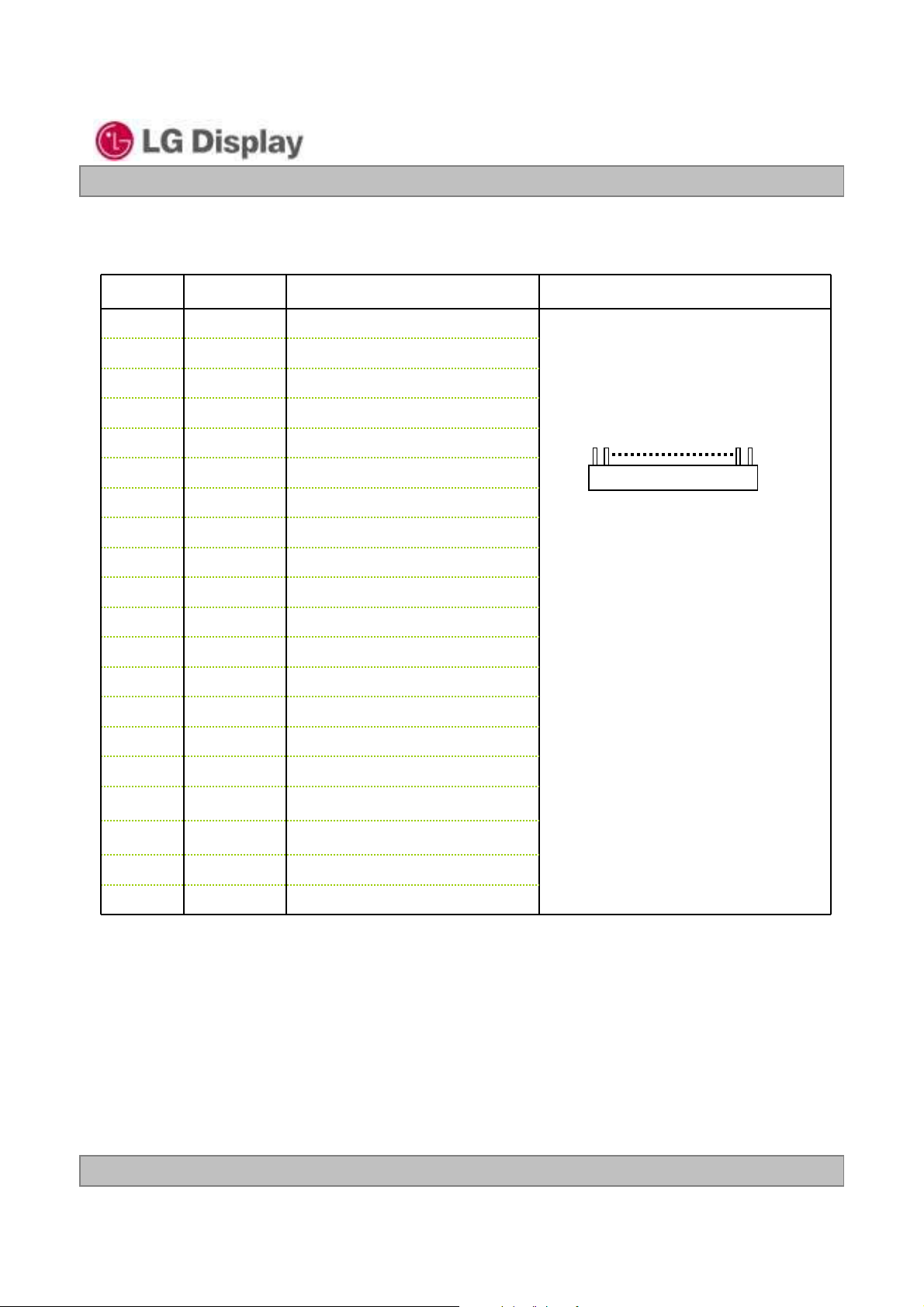
This LCD employs two interface connections, a 50 pin connector is used for the module electronics interface
and the other connector is used for the integral backlight system.
Table 3. MODULE CONNECTOR PIN CONFIGURATION (CN1
Pin Symbol Description
1 GND Ground
2 AVDD Power Supply, 3.3V Typ.
3 AVDD Power Supply, 3.3V Typ.
4 AVDD Power Supply, 3.3V Typ.
5 AVDD Power Supply, 3.3V Typ.
6 AVDD Power Supply, 3.3V Typ.
7 AVDD Power Supply, 3.3V Typ.
8 AVDD Power Supply, 3.3V Typ.
9 DVDD Digital Power supply (3.3V Typ)
10 DVDD Digital Power supply (3.3V Typ)
11 BIST BIST
12 Clk EEDID Two wire serial interface clock
13 DATA EEDID Two wire serial interface data
14 GND Ground
15 RXinO0- - LVDS differential data input, Chan 0-Odd
16 RXinO0+ + LVDS differential data input, Chan 0-Odd
17 GND Ground
18 RXinO1 - LVDS differential data input, Chan 1-Odd
19 RXinO1+ + LVDS differential data input, Chan 1-Odd
20 GND Ground
21 RXinO2- - LVDS differential data input, Chan 2-Odd
22 RXinO2+ + LVDS differential data input, Chan 2-Odd
23 GND Ground
24 RXOC- - LVDS Differential Clock input (Odd)
25 RX OC+ + LVDS Differential Clock input (Odd)
26 GND Ground
27 RXinO3- - LVDS differential data input, Chan 3-Odd
28 RXinO3+ + LVDS differential data input, Chan 3-Odd
29 GND Ground
30 RXinO4- - LVDS differential data input, Chan 4-Odd
31 RXinO4+ + LVDS differential data input, Chan 4-Odd
32 GND Ground
33 RXinE0- - LVDS differential data input, Chan 0-Even
34 RXinE0+ + LVDS differential data input, Chan 0-Even
35 GND Ground
36 RXinE1- - LVDS differential data input, Chan 1-Even
37 RXinE1+ + LVDS differential data input, Chan 1-Even
38 GND Ground
39 RXinE2- - LVDS differential data input, Chan 2-Even
40 RXinE2+ + LVDS differential data input, Chan 2-Even
41 GND Ground
42 RXEC- - LVDS Differential Clock input (Even)
43 RXEC+ + LVDS Differential Clock input (Even)
44 GND Ground
45 RXinE3- - LVDS differential data input, Chan 3-Even
46 RXinE3+ + LVDS differential data input, Chan 3-Even
47 GND Ground
48 RXinE4- - LVDS differential data input, Chan 4-Even
49 RXinE4+ + LVDS differential data input, Chan 4-Even
50 GND Ground
)
Notes
1, Interface chips
1.1 LCD : LGE (MAKO)
including LVDS Receiver,
VESA LVDS 10bit Format
1.2 System :
* Pin to Pin compatible with LVDS
2.Connector
2.1 LCD : JAE FI-VHP50S-A-HF11
or equivalent
2.2 Mating: JAE or equivalent
2.3 Connector pin arrangement
LCD rear view
1
[LCD Module Rear View]
50
Ver. 1.1
Ver. 1.1
20. Oct. 2011
20. Oct. 2011
7 / 34
Page 8
Product Specification
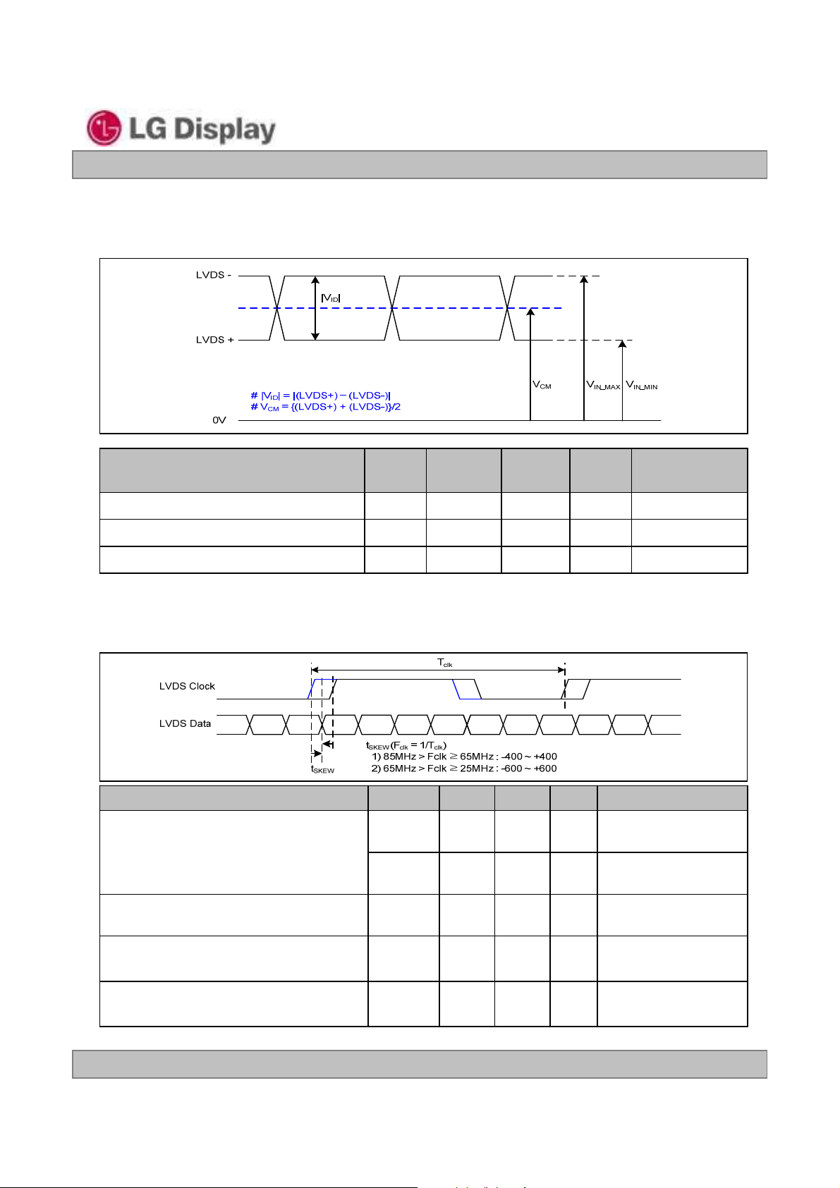
3-3. LVDS Signal Timing Specifications
3-3-1. DC Specification
LP173WF3
Liquid Crystal Display
Description
LVDS Differential Voltage |V
LVDS Common mode Voltage V
LVDS Input Voltage Range V
3-3-2. AC Specification
Description Symbol Min Max Unit Notes
LVDS Clock to Data Skew Margin
Symb
ol
| 100 600 mV -
ID
CM
IN
t
SKEW
t
SKEW
Min Max Unit Notes
0.6 1.8 V -
0.3 2.1 V -
- 400 + 400 ps
- 600 + 600 ps
85MHz > Fclk ≥
65MHz > Fclk ≥
65MHz
25MHz
LVDS Clock to Clock Skew Margin (Even
to Odd)
Maximum deviation
of input clock frequency during SSC
Maximum modulation frequency
of input clock during SSC
Ver. 1.1
Ver. 1.1
t
SKEW_EO
F
DEV
F
MOD
20. Oct. 2011
20. Oct. 2011
-1/7 + 1/7 T
clk
-
- ± 3% -
-200KHz -
8 / 34
Page 9
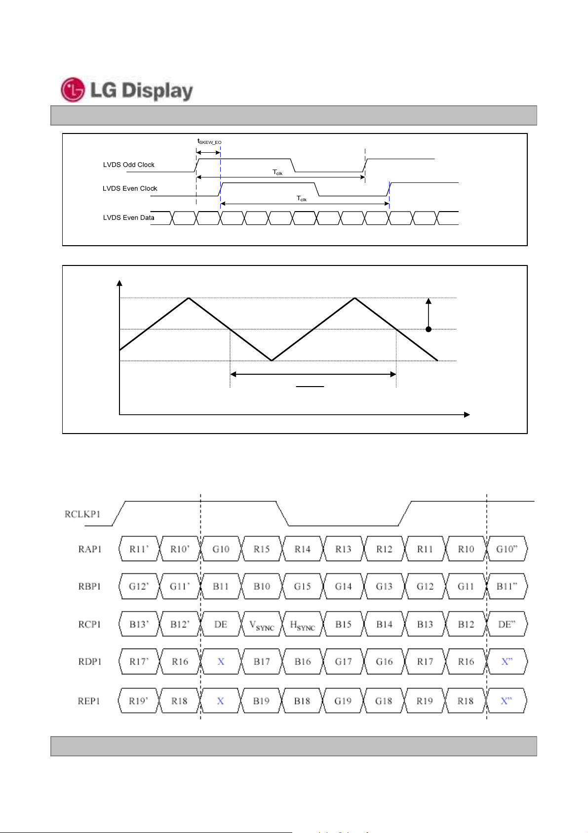
Freq.
F
max
F
center
F
min
Product Specification
< Clock skew margin between channel >
LP173WF3
Liquid Crystal Display
F
* F
center
DEV
3-3-3. Data Format
1) LVDS Data Port
1
F
MOD
< Spread Spectrum >
Time
Ver. 1.1
Ver. 1.1
< LVDS Data Format >
20. Oct. 2011
20. Oct. 2011
9 / 34
Page 10
Liquid Crystal Display
Product Specification
Table 4. BACKLIGHT CONNECTOR PIN CONFIGURATION (CN2)
Pin Symbol Description Notes
1 GND Ground
LP173WF3
2 VBL+ 7V - 20V LED Power
3 VBL+ 7V - 20V LED Power
4 VBL+ 7V - 20V LED Power
5 VBL+ 7V - 20V LED Power
6 VBL+ 7V - 20V LED Power
7VBL-Ground
8VBL-Ground
9VBL-Ground
10 VBL- Ground
11 VBL- Ground
12 NC No Connection
13 GND Ground
14 I2C_DATA DATA for RGB control
15 I2C_CLK CLK for RGB control
16 GND Ground
17 BL_Enable
18 BLIM
19 Reserved Reserved
BL On/Off Control
(On: 3.0V ~ 3.6V, Off: 0V ~ 0.5V)
PWM for Luminance Control
(200~1KHz, 3.3V, 5~100%) or DC(0~3.3v)
1. Connector
1.1 LCD : Hirose DF19KR
or equivalent
1.2 Mating : Hirose equivalent.
1.3 Connector pin arrangement
1
[LCD Module Rear View]
20
20 GND Ground
Ver. 1.1
Ver. 1.1
20. Oct. 2011
20. Oct. 2011
10 / 34
Page 11
LP173WF3
Liquid Crystal Display
Product Specification
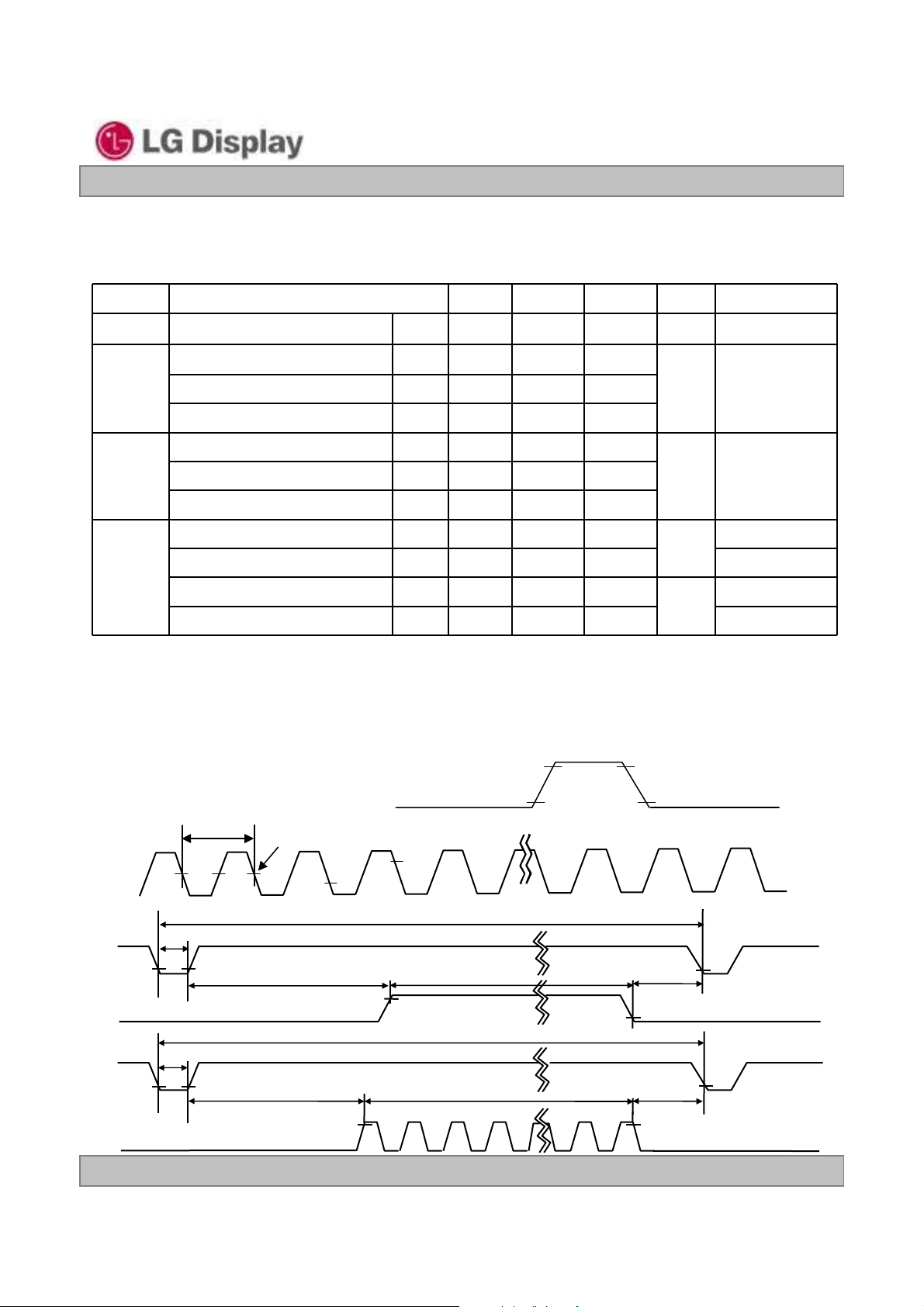
3-3. Signal Timing Specifications
This is the signal timing required at the input of the User connector. All of the interface signal timing should be
satisfied with the following specifications and specifications of LVDS Tx/Rx for its proper operation.
Table 5. TIMING TABLE
ITEM Symbol Min Typ Max Unit Note
DCLK Frequency f
Period
Hsync
Width t
Width-Active t
Period t
Vsync
Width-Active t
Horizontal back porch t
Data
Enable
Horizontal front porch t
Vertical back porch t
Vertical front porch t
CLK
t
WH
WHA
WV
WVA
HBP
HFP
VBP
VFP
67.17 69.35 72.65 MHz LVDS 2 Port
HP
1020 1040 1078
16 16 16
tCLK
960 960 960
VP
1096 1111 1122
55 5
tHPWidth t
1080 1080 1080
34 40 50
tCLK
10 24 52
10 23 28
tHP
13 9
Appendix) 1) All reliabilities are specified for timing specification based on r efresh rate of 60 Hz. Even though actual
performance in 50Hz and 48Hz for low power is displayed normally, remark and inform to user that display quality in
50 Hz and 48 Hz is out of guarantee range.
2) Timing is controlled by EEDID Timing at refresh rate of 60Hz. All display quality is guaranteed based on refresh rate
of 60Hz controlled by EEDID timing.
3-4. Signal Timing Waveforms (Normal status)
High: 0.7VCC
Condition : VCC =3.3V
Data Enable, Hsync, Vsy n c
Low: 0.3VCC
DCLK
Hsync
t
Data Enable
Vsync
Data Enable
Ver. 1.1
Ver. 1.1
t
WH
WV
tCLK
t
VBP
t
HBP
0.5 Vcc
t
HP
t
VP
20. Oct. 2011
20. Oct. 2011
tWHA
tWVA
t
HFP
t
VFP
11 / 34
Page 12
LP173WF3
Liquid Crystal Display
Product Specification
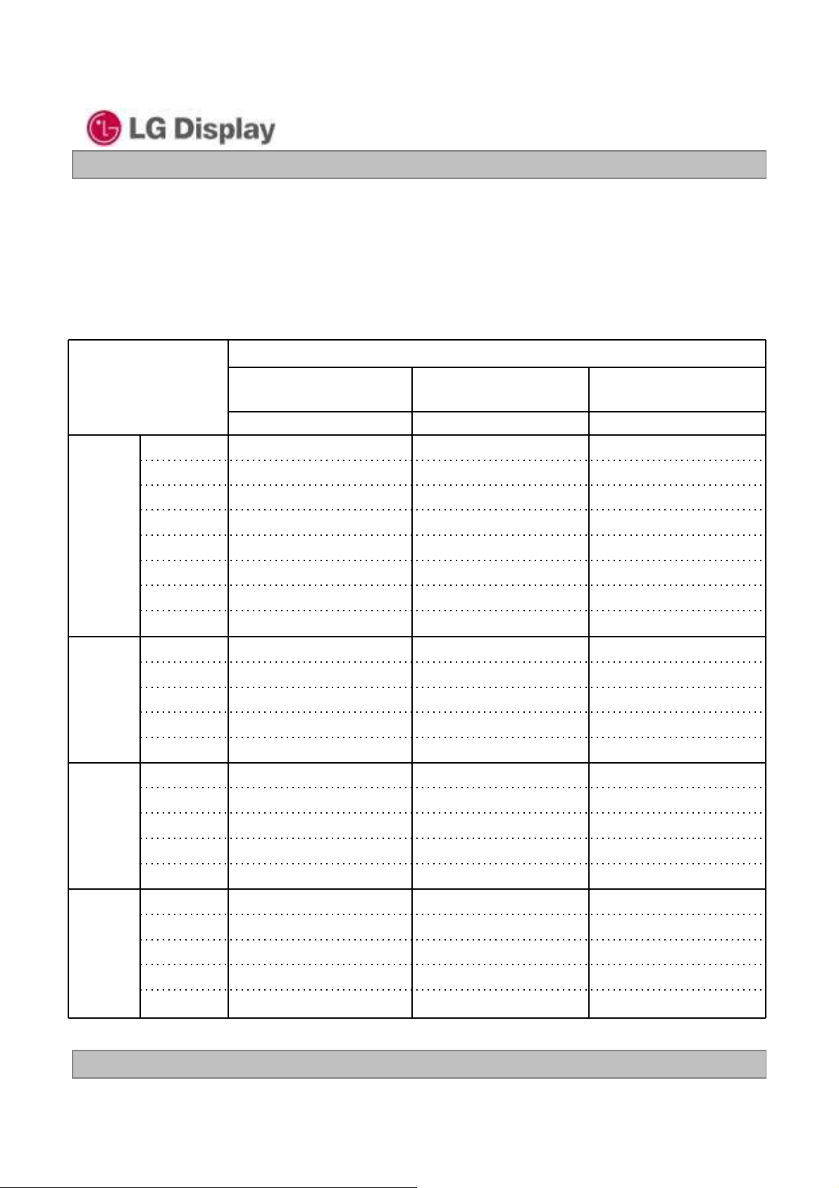
3-5. Color Input Data Reference
The brightness of each primary co lor (r ed,green and blue) is based on the 10-bit gray scale data input for the
color ; the higher the binary input, the brighter the color. The table below provides a reference for color
versus data input.
Table 6. COLOR DATA REFERENCE
Input Color Data
Basic
Color
RED
Color
Black
Red (1023)
Green (1023)
Blue (1023)
Cyan
Magenta
Yellow
White
RED (000)
RED (001)
...
RED (1022)
RED (1023)
GREEN (000)
RED
MSB LSB
R9 R8 R7 R6 R5 R4 R3 R2 R1 R0 G9 G8 G7 G6 G5 G4 G3 G2 G1 G0 B9 B8 B7 B6 B5 B4 B3 B2 B1 B0
0 0 0 0 0 0 0 0 0 0 0 0 0 0 0 0 0 0 0 0 0 0 0 0 0 0 0 0 0 0
1 1 1 1 1 1 1 1 1 1 0 0 0 0 0 0 0 0 0 0 0 0 0 0 0 0 0 0 0 0
0 0 0 0 0 0 0 0 0 0 1 1 1 1 1 1 1 1 1 1 0 0 0 0 0 0 0 0 0 0
0 0 0 0 0 0 0 0 0 0 0 0 0 0 0 0 0 0 0 0 1 1 1 1 1 1 1 1 1 1
0 0 0 0 0 0 0 0 0 0 1 1 1 1 1 1 1 1 1 1 1 1 1 1 1 1 1 1 1 1
1 1 1 1 1 1 1 1 1 1 0 0 0 0 0 0 0 0 0 0 1 1 1 1 1 1 1 1 1 1
1 1 1 1 1 1 1 1 1 1 1 1 1 1 1 1 1 1 1 1 0 0 0 0 0 0 0 0 0 0
1 1 1 1 1 1 1 1 1 1 1 1 1 1 1 1 1 1 1 1 1 1 1 1 1 1 1 1 1 1
0 0 0 0 0 0 0 0 0 0 0 0 0 0 0 0 0 0 0 0 0 0 0 0 0 0 0 0 0 0
0 0 0 0 0 0 0 0 0 1 0 0 0 0 0 0 0 0 0 0 0 0 0 0 0 0 0 0 0 0
... ... ...
1 1 1 1 1 1 1 1 1 0 0 0 0 0 0 0 0 0 0 0 0 0 0 0 0 0 0 0 0 0
1 1 1 1 1 1 1 1 1 1 0 0 0 0 0 0 0 0 0 0 0 0 0 0 0 0 0 0 0 0
0 0 0 0 0 0 0 0 0 0 0 0 0 0 0 0 0 0 0 0 0 0 0 0 0 0 0 0 0 0
MSB LSB
GREEN
BLUE
MSB LSB
GREEN
BLUE
Ver. 1.1
Ver. 1.1
GREEN (001)
...
GREEN (1022)
GREEN (1023)
BLUE (000)
BLUE (001)
...
BLUE (1022)
BLUE (1023)
0 0 0 0 0 0 0 0 0 0 0 0 0 0 0 0 0 0 0 1 0 0 0 0 0 0 0 0 0 0
... ... ...
0 0 0 0 0 0 0 0 0 0 1 1 1 1 1 1 1 1 1 0 0 0 0 0 0 0 0 0 0 0
0 0 0 0 0 0 0 0 0 0 1 1 1 1 1 1 1 1 1 1 0 0 0 0 0 0 0 0 0 0
0 0 0 0 0 0 0 0 0 0 0 0 0 0 0 0 0 0 0 0 0 0 0 0 0 0 0 0 0 0
0 0 0 0 0 0 0 0 0 0 0 0 0 0 0 0 0 0 0 0 0 0 0 0 0 0 0 0 0 1
... ... ...
0 0 0 0 0 0 0 0 0 0 0 0 0 0 0 0 0 0 0 0 1 1 1 1 1 1 1 1 1 0
0 0 0 0 0 0 0 0 0 0 0 0 0 0 0 0 0 0 0 0 1 1 1 1 1 1 1 1 1 1
20. Oct. 2011
20. Oct. 2011
12 / 34
Page 13
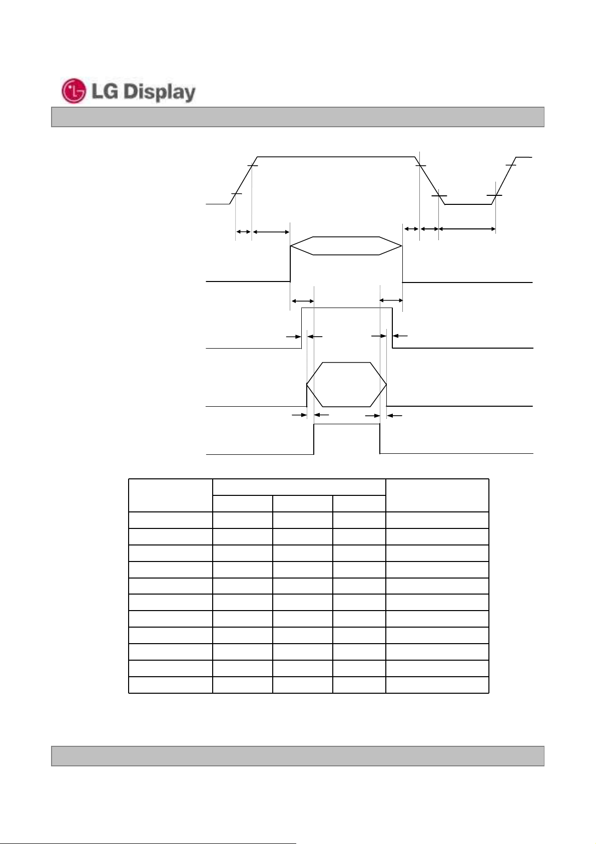
3-6. Power Sequence
Power Supply Input
VCC
0V
Product Specification
90%
LP173WF3
Liquid Crystal Display
90%
10%10%
T
7
Interface Signal, V
T
T
6
T
T
1
i
2
Valid Data
5
LVDS
0V
T
3
T
4
LED input Voltage
VLED
T
8
T
11
0V
Dimming control signal
Of LED BL
0V (Low)
Valid Data
PWM
LED on/off control Signal
LED_EN
0V (Off)
T
9
T
10
Table 6. POWER SEQUE NCE TABLE
Value
Units
Note)
Parameter
T
1
T
2
T
3
T
4
T
5
T
6
T
7
T
8
T
9
T
10
T
11
Min. Typ. Max.
0.5 - 10 ms
0-50 ms
300 - - ms
300 - - ms
0-50 ms
3-10 ms
400 - - ms
10 - - ms
10 - - ms
10 - - ms
10 - - ms
1. Valid Data is Data to meet “3-3. LVDS Signal Timing Specifications”
2. Please avoid floating state of interface signal at invalid period.
3. When the interface signal is invalid, be sure to pull down the power supply for LCD VCC to 0V.
4. Lamp power must be turn on after power supply for LCD and interface signal are valid.
Ver. 1.1
Ver. 1.1
20. Oct. 2011
20. Oct. 2011
13 / 34
Page 14
LP173WF3
Liquid Crystal Display
Product Specification
4. Optical Specification
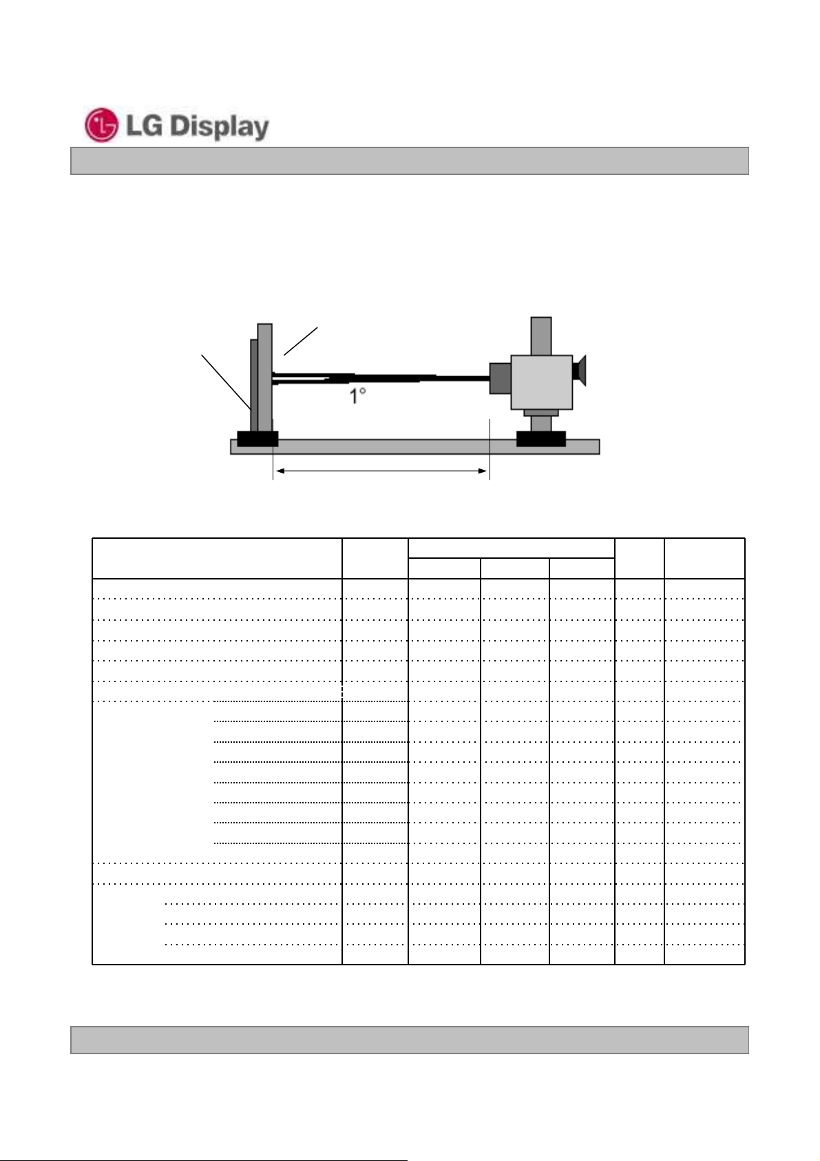
Optical characteristics are deter mined after the unit has been ‘ON ’ and stable for approximately 30 minutes in
a dark environment at 25
at a viewing angle of
FIG. 1 presents additional information concerning the measurement equipment and method.
C. The values specified are at an approximate distance 50cm from the LC D su rface
and equal to 0.
FIG. 1 Optical Characteristic Measurement Equipment and Method
Optical Stage(x,y)
LCD Module
Pritchard 880 or
equivalent
50cm
Table 8. OPTICAL CHARACTERISTICS
Ta=25C, VCC=3.3V, fV=60Hz, f
Parameter Symbol
Contrast Ratio CR 600 800 - 1
Surface Luminance, white L
Luminance Variation
Response Time 4
Rise Time+Decay Time (W to B) Tr
Color Coordinates
RED RX
GREEN GX
BLUE BX
WHITE WX 0.283 0.313 0.343
Viewing Angle 5
x axis, right(=0) r
x axis, left (=180) l
y axis, up (=90) u
y axis, down (=270) d
WH
WHITE
R +TrD
RY
GY
BY
WY 0.299 0.329 0.359
= 69.35MHz(LVDS 2Port), Finished Color Calibration
CLK
Values
Min Typ Max
250 300 - cd/m
-1.41.6 3
-3550ms
0.652 0.682 0.712
0.275 0.305 0.335
0.169 0.199 0.229
0.691 0.721 0.751
0.121 0.151 0.181
0.015 0.045 0.075
80 89 - degree
80 89 - degree
80 89 - degree
80 89 - degree
Units Notes
2
2
Ver. 1.1
Ver. 1.1
20. Oct. 2011
20. Oct. 2011
14 / 34
Page 15
Liquid Crystal Display
Product Specification
Note)
1. Contrast Ratio(CR) is defined mathematically as
Surface Luminance with all white pixels
Contrast Ratio =
Surface Luminance with all black pixels
2. Surface luminance is the 5point (1~5)average across the LCD surface 50cm from the surface
with all pixels displaying white Luminance (300nit). For more information see FIG 2.
3. Luminance % uniformity is measured for 13 point For more information see FIG 2.
δ WHITE = Maximum(LN1,LN2, ….. LN13) ÷ Minimum(LN1,LN2, ….. LN13)
LP173WF3
4. Response time is the time required for the display to transition from white to black (rise time, Tr
from black to white(Decay Time, Tr
). For additional information see FIG 3.
D
) and
R
5. Viewing angle is the angle at which the contrast ratio is greater than 10. The angles are determined
for the horizontal or x axis and the vertical or y axis with respect to the z axis which is normal to the
LCD surface. For more information see FIG 4.
6. Gray scale specification * f
=60Hz
V
Gray Level Luminance [%] (Typ)
L0
L63
L127
L191
L255
L319
L383
L447
L511
L575
L639
L703
L767
L831
L895
L959
L1023
0.10
0.23
0.79
2.13
4.49
7.70
11.7
16.3
21.4
27.9
35.2
43.1
51.8
62.1
74.4
87.6
100
Ver. 1.1
Ver. 1.1
-. △L Reference Level : 16 steps from gray 0 to gray 1023
20. Oct. 2011
20. Oct. 2011
15 / 34
Page 16
Product Specification
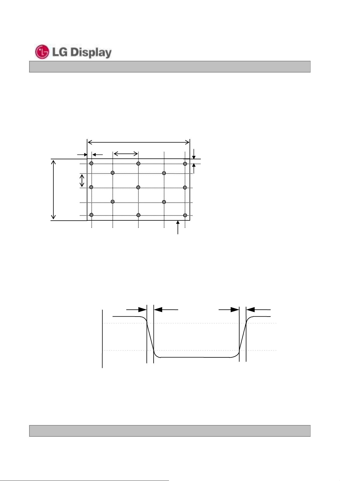
FIG. 2 Luminance
<measuring point for surface luminance & measuring point for luminance variation>
H
LP173WF3
Liquid Crystal Display
10mm
678
B
V
910
11 12
A
10mm
2
1
4
3
5
13
Active Ar e a
H,V
: ACTIVE AR EA
A : H/4 mm
B: V/4 mm
POINTS: 13 POINTS
FIG. 3 Response Time
The response time is defined as the following figure and shall be measured by switching the input signal
for “black” and “white” In condition of RGB LED Duty 100%
Tr
Tr
R
D
%
100
90
Optical
Response
10
0
white
white
black
In other condition (For example, RGB LED Duty 80%), The response time defined as measurement data
which is not lack
Ver. 1.1
Ver. 1.1
20. Oct. 2011
20. Oct. 2011
16 / 34
Page 17
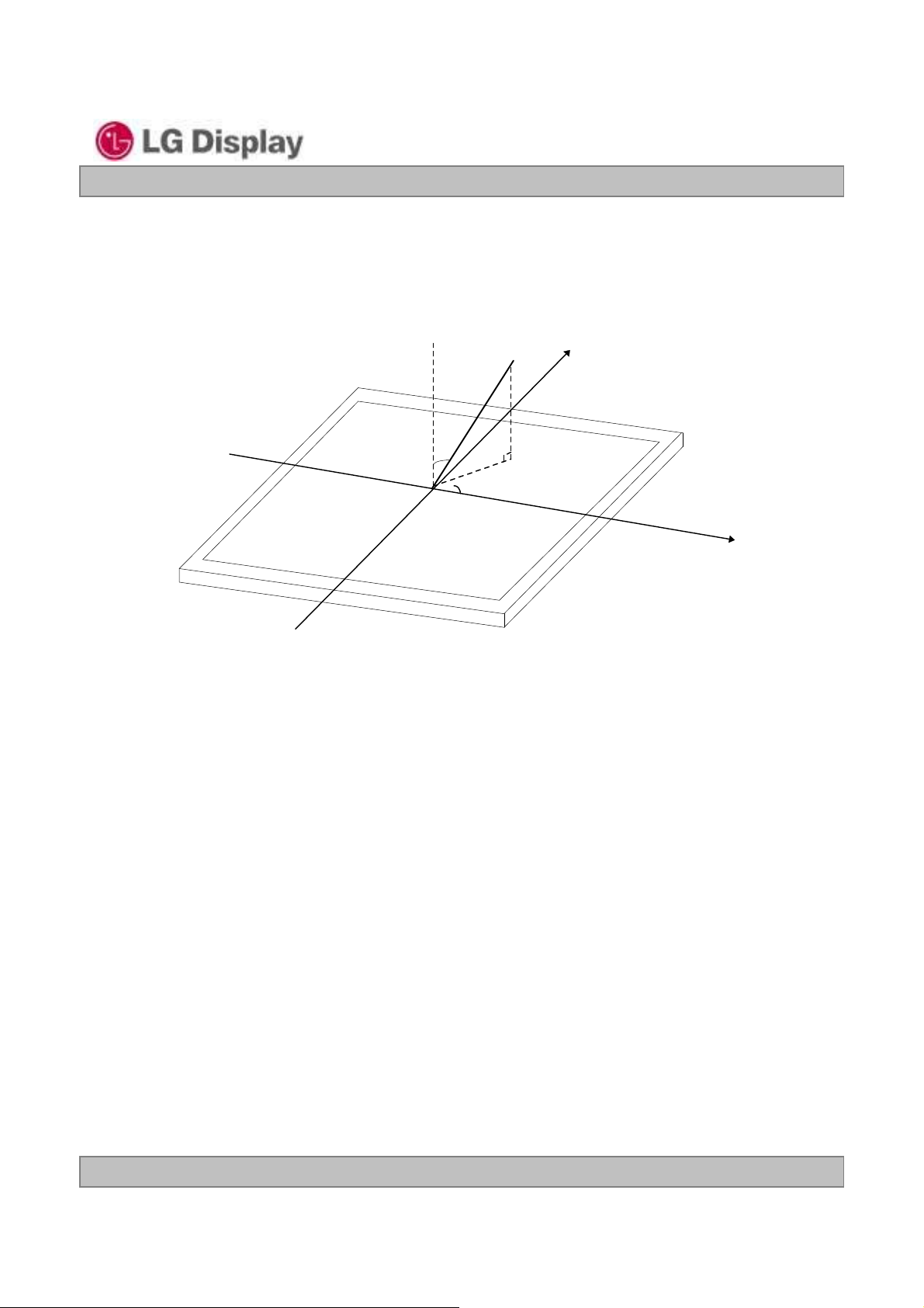
FIG. 4 Viewing angle
LP173WF3
Liquid Crystal Display
Product Specification
<Dimension of viewing angle range>
= 180
= 270
,
Left
Down
Normal
Eye
Y
= 90, Up
Right
,
= 0
,
Ver. 1.1
Ver. 1.1
20. Oct. 2011
20. Oct. 2011
17 / 34
Page 18
LP173WF3
Liquid Crystal Display
Product Specification
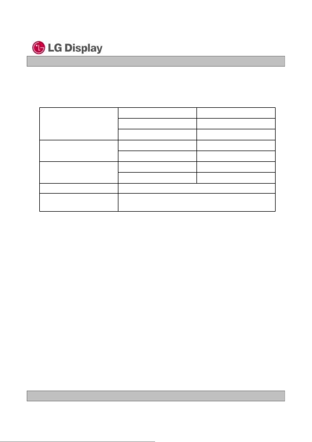
5. Mechanical Characteristics
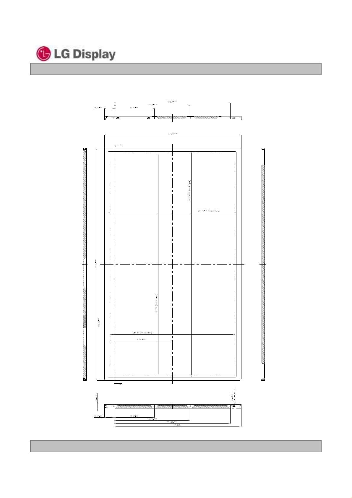
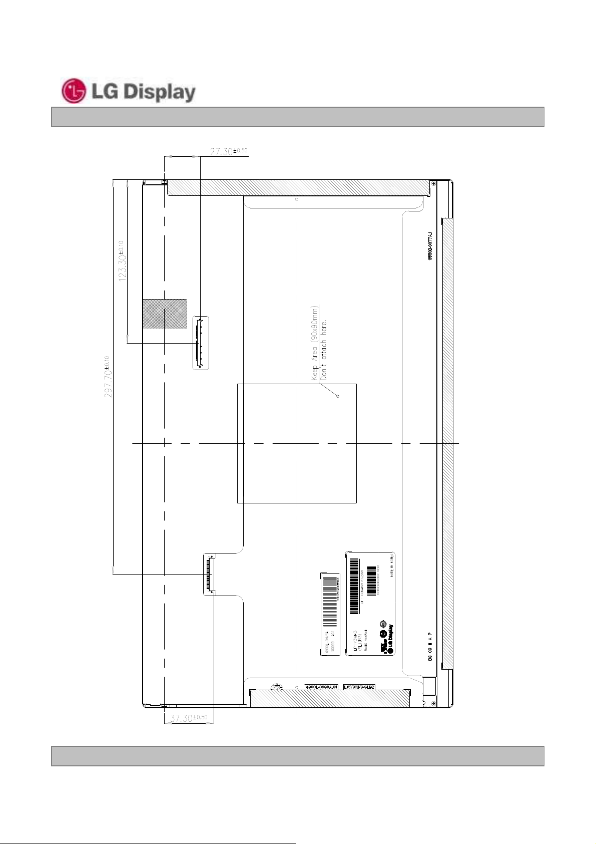
The contents provide general mechanical characteristics for the model LP173WF3(SLB3). In addition the
figures in the next page are detailed mechanical drawing of the LCD.
Horizontal 398.1 ± 0.5 mm
Outline Dimension
Bezel Area
Active Display Area
Weight 830 g (MAX)
Surface Treatment Hard coating(3H), Anti-Glare treatment of the front polarizer
Vertical 234.3 ± 0.5 mm
Depth (Max) 7.2 mm
Horizontal 386.70(H)
Vertical 219.75(V)
Horizontal 381.90 mm
Vertical 214.80 mm
Ver. 1.1
Ver. 1.1
20. Oct. 2011
20. Oct. 2011
18 / 34
Page 19
Product Specification
LP173WF3
Liquid Crystal Display
<FRONT VIEW>
Note) Unit:[mm], General tolerance:
0.5mm
Ver. 1.1
Ver. 1.1
20. Oct. 2011
20. Oct. 2011
19 / 34
Page 20
Product Specification
LP173WF3
Liquid Crystal Display
<REAR VIEW>
Note) Unit:[mm], General tolerance:
0.5mm
Ver. 1.1
Ver. 1.1
20. Oct. 2011
20. Oct. 2011
20 / 34
Page 21
Product Specification
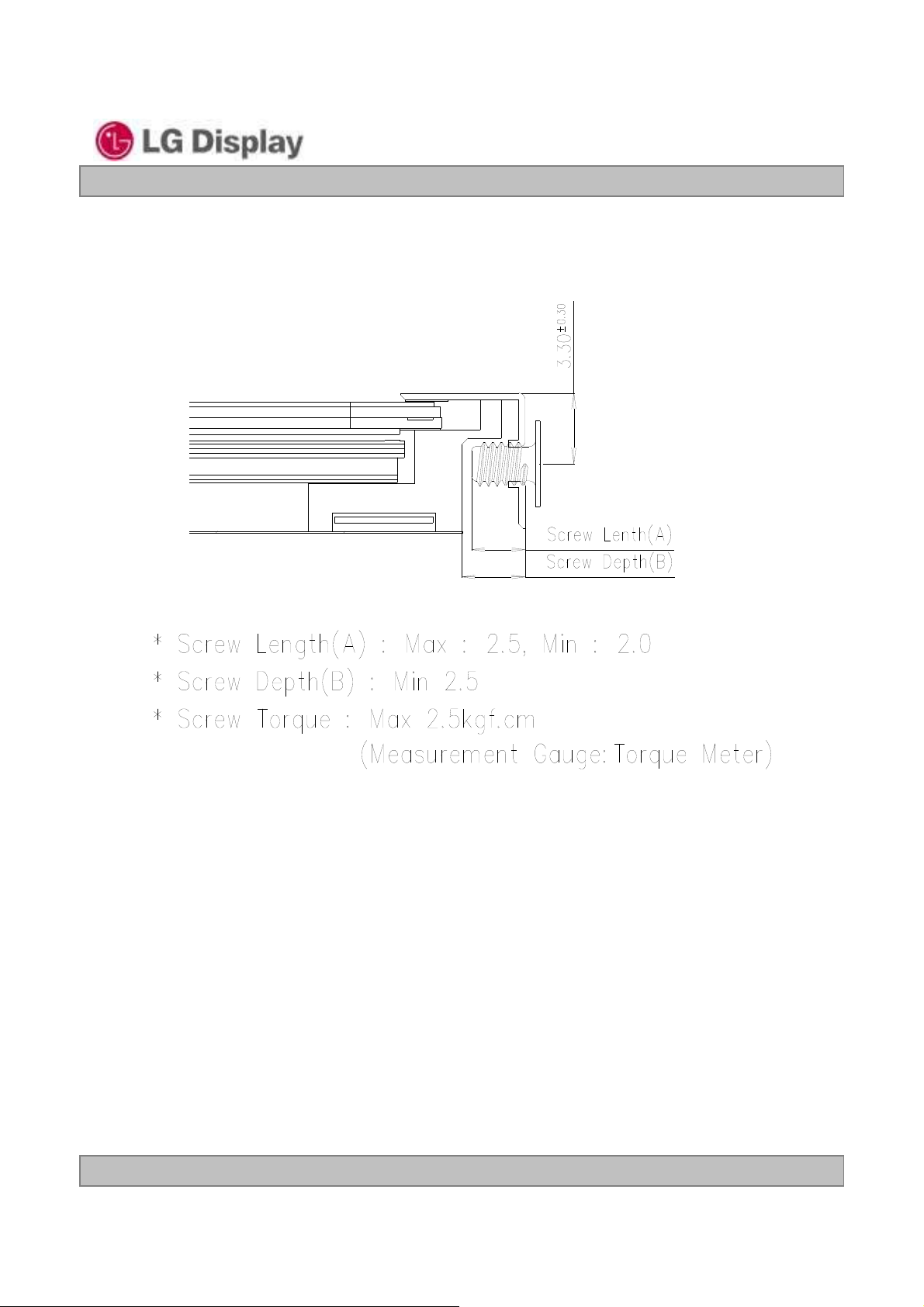
[ DETAIL DESCRIPTION OF SIDE MOUNTING SCREW ]
LP173WF3
Liquid Crystal Display
Notes : 1. Screw plated through the method of non-electrolytic nickel plating is preferred
to reduce possibility that results in vertical and/or horizontal line defect due to
the conductive particles from screw surface.
Note) Unit:[mm], General tolerance:
Ver. 1.1
Ver. 1.1
20. Oct. 2011
20. Oct. 2011
0.5mm
21 / 34
Page 22
Product Specification
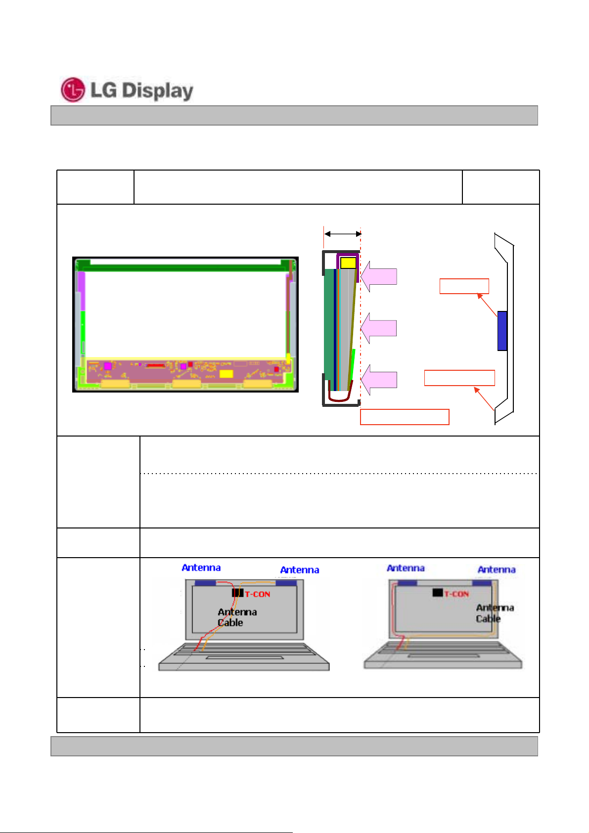
LGD Proposal for system cover design.(Appendix)
LP173WF3
Liquid Crystal Display
1
Gap check for securing the enough gap between LCM
and System cover.
Max Thickness
Sponge
LCM Reflector Side
System Cover
A Boundary Line
1.Rear side of LCM is sensitive against external stress,and previous check
about interference is highly needed.
Define
Define
Ver. 1.1
Ver. 1.1
2.In case there is something from system cover comes into the boundary
above,mechanical interference may cause the FOS defects.
(Eg:Ripple,White spot..)
2 Check if antenna cable is sufficiently apart from T-CON of LCD Module.
NO GOOD
GOOD
1.If system antenna is overlapped with T-CON,it might be cause the noise.
20. Oct. 2011
20. Oct. 2011
22 / 34
Page 23
Product Specification
LGD Proposal for system cover design.
LP173WF3
Liquid Crystal Display
3
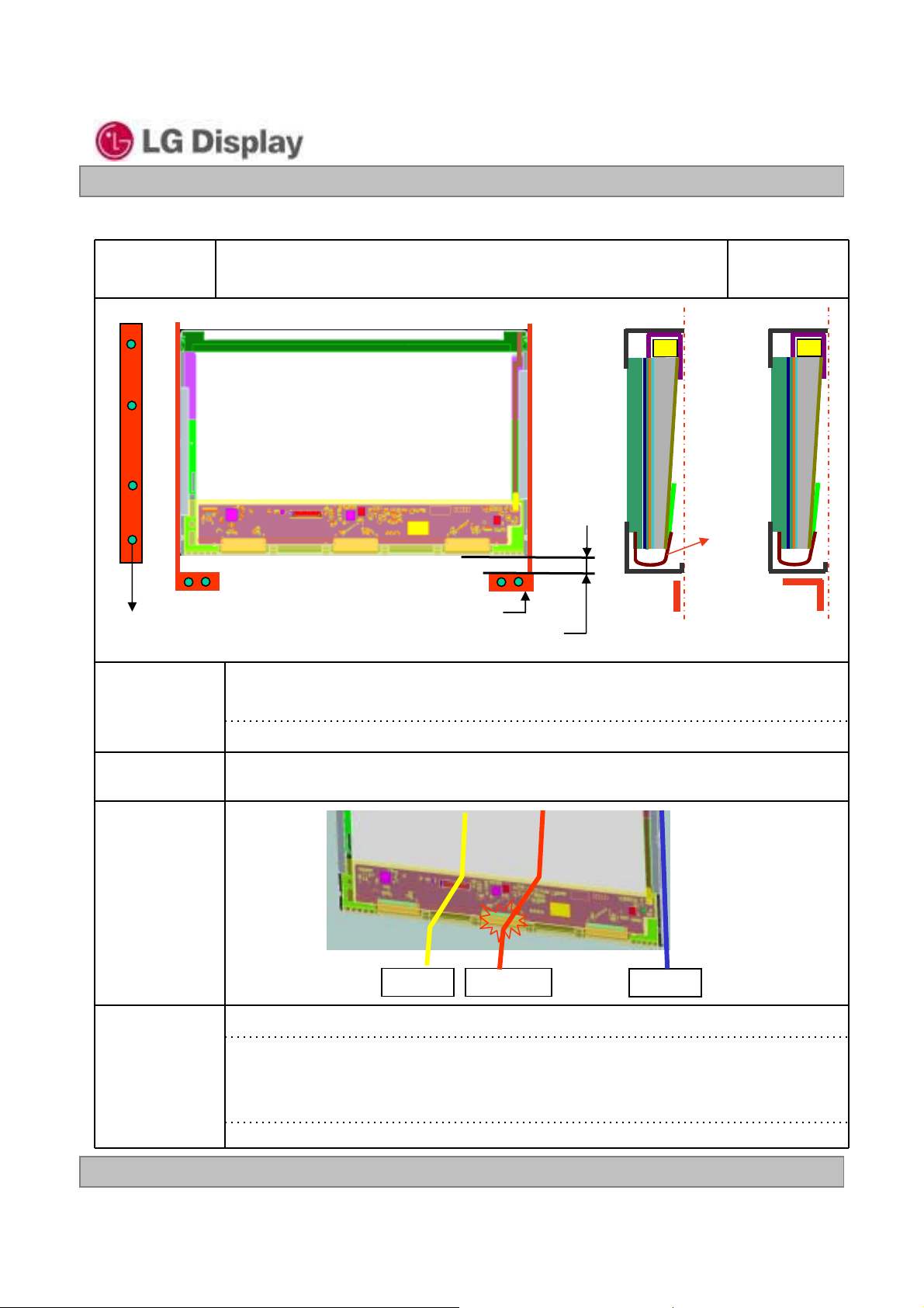
Gap check for securing the enough gap between LCM
and System hinge.
LCM Reflector Side
Side Mount Screw Hole (4ea)
1.At least 2.0mm of gap needs to be secured to prevent the shock
Define
related defects.
Hinge
GAP:Min2.0mm
(“I” TYPE)
COF
(D-IC)
(“L” TYPE)
Define
Ver. 1.1
Ver. 1.1
2.”L” type of hinge is recommended than “I” type under shock test.
4
Checking the path of the System wire.
#3
#2
Ok Bad
#1
Good
1.COF area needs to be handled with care.
2.GOOD Wire path design to system side.
OK Wire path is located between COFs.
BADWire path overlapped with COF area.
20. Oct. 2011
20. Oct. 2011
23 / 34
Page 24
Product Specification
LGD Proposal for system cover design.
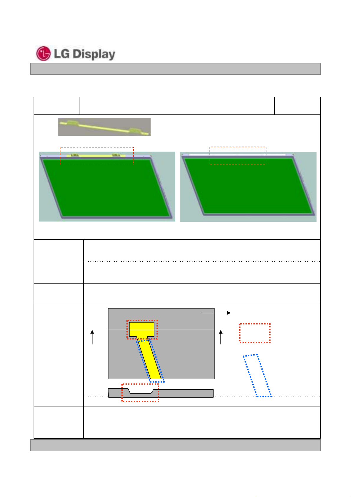
5 Using a bracket on the top of LCM is not recommended.
bracket
LP173WF3
Liquid Crystal Display
With bracket Without bracket
1.Condition without bracket is good for mechanical noise,and can minimize
the light leakage from deformation of bracket.
Define
2.The results shows that there is no difference between the condition
with or without bracket.
6 Securing additional gap on CNT area..
A
A~A-1
cut
System cover inner side.
User connector
area.
A-1
User connector
Cable pathway.
FPC:Flexible Printed Circuit.
Define
Ver. 1.1
Ver. 1.1
1.CNT area is specially sensitive against external stress,and additional
gap by cutting on system cover will be helpful on removing the Ripple.
2.Using a thinner CNT will be better. (eg: FPC type)
20. Oct. 2011
20. Oct. 2011
24 / 34
Page 25
Product Specification
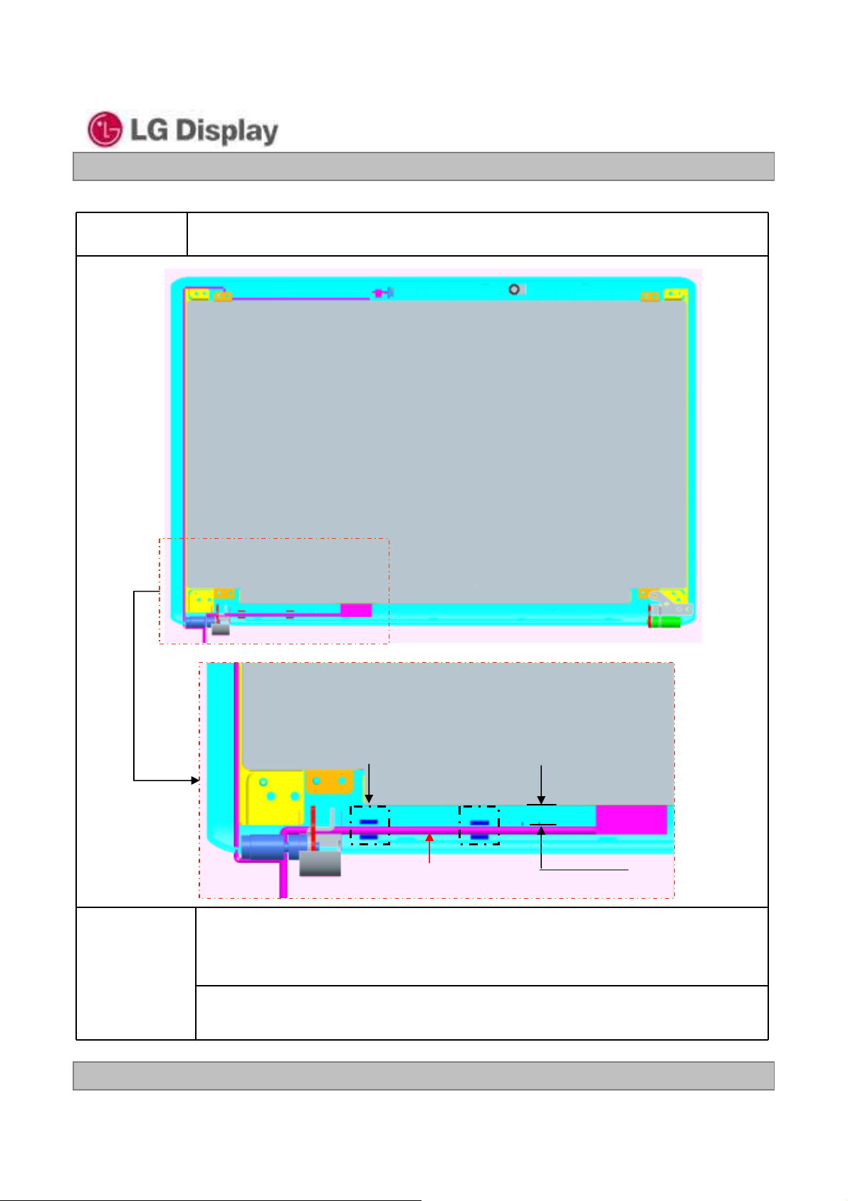
7 Checking the path of the System LVDS Cable.
See Detail “A”
LP173WF3
Liquid Crystal Display
Define
Ver. 1.1
Ver. 1.1
Detail “A”
LVDS Cable Guide
PCB
Connector
Ⓐ
LVDS Cable
1.At least 1.0mm of gap needs to be secured to prevent the overlap
between LVDS cable and PCB.(Ⓐ ≥ 1.0mm)
(This overlap may cause a Abnormal Display after hinge test)
2.”Flat” type of LVDS cable is recommended than “Cylinderical” type .
3. Making LVDS Cable Guide will be better.(Refer to detail “A”)
20. Oct. 2011
20. Oct. 2011
25 / 34
Page 26
Liquid Crystal Display
Product Specification
LGD Proposal for system cover design.
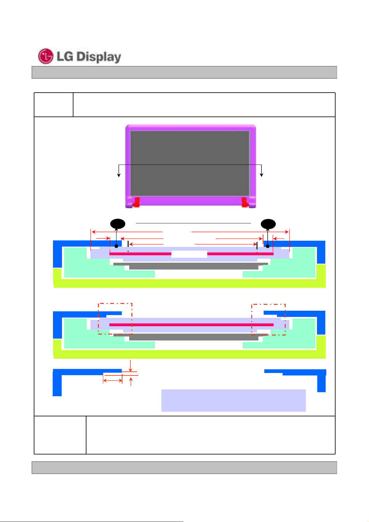
8 Securing additional gap between front cover & LCD at edge of front cover.
LP173WF3
No Good
Front Cover
Good
Front Cover
Supporter Main
Back Cover
Supporter Main
Back Cover
“A”
A
“A” : Overlap between Front Cover & Liquid Crystal area
Panel Size
Front Bezel Open Size
Active Area
Cell
Liquid Crystal
A
“A”
Define
Ver. 1.1
Ver. 1.1
Recess Depth(Ⓑ) : ?.?mm
Resses Width(Ⓐ) : ?.?mm
※ Recess Width(Ⓐ) : Up / Down /Left /Right
※ Recess Depth(Ⓑ) : Up / Down /Left /Right
1.Liquid Crystal area is sensitive against external stress, so additional
gap by making recess area at the edge of front cover will be helpful on
removing a Ripple.(Dimension of Recess depends on each model)
20. Oct. 2011
20. Oct. 2011
26 / 34
Page 27
Liquid Crystal Display
Product Specification
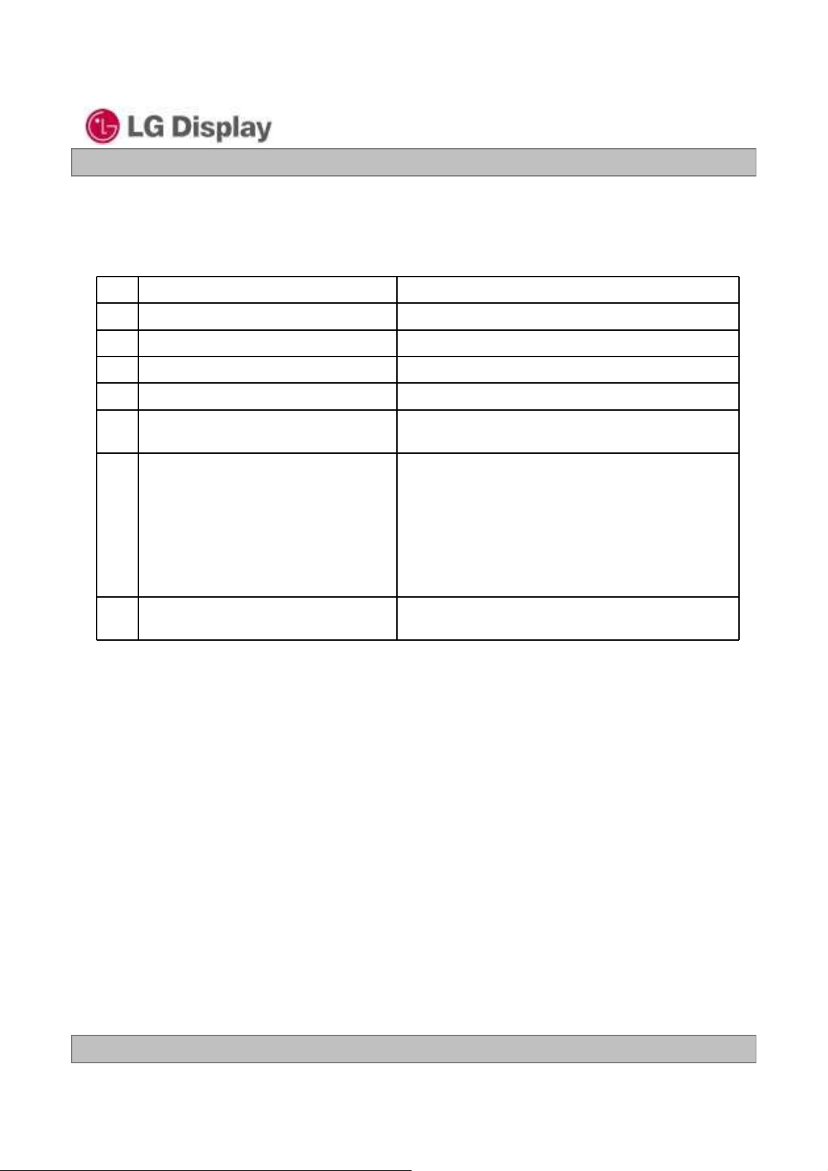
6. Reliability
Environment test condition
No. Test Item Conditions
1 High temperature storage test Ta= 60C, 240h
2 Low temperature storage test Ta= -20C, 240h
3 High temperature operation test Ta= 50C, 50%RH, 240h
4 Low temperature operation test Ta= 0C, 240h
5 Vibration test (non-operating) Sine wave, 5 ~ 150Hz, 1.5G, 0.37oct/min
3 axis, 30min/axis
6 Shock test (non-operating) - No functional or cosmetic defects following a shock
to all 6 sides delivering at least 200 G in a half sine
pulse no longer than 2 ms to the display module
- No functional defects following a shock delivering
at least 260 g in a half sine pulse no longer than 2
ms to each of 6 sides. Each of the 6 si des will be
shock tested with one each display, for a total of 6
displays
LP173WF3
7 Altitude operating
storage / shipment
0 ~ 10,000 feet (3,048m) 24Hr
0 ~ 40,000 feet (12,192m) 24Hr
{ Result Evaluation Criteria }
There should be no change which might affect the practical display function when the display quality
test is conducted under normal operating condition.
Ver. 1.1
Ver. 1.1
20. Oct. 2011
20. Oct. 2011
27 / 34
Page 28

LP173WF3
Liquid Crystal Display
Product Specification
7. International Standards
7-1. Safety
a) UL 60950-1, Second Edition, Underwriters Laboratories Inc.
Information Technology Equipment - Safety - Part 1 : General Requirements.
b) CAN/CSA C22.2 No.60950-1-07, Second Edition, Canadian Standards Association.
Information Technology Equipment - Safety - Part 1 : General Requirements.
c) EN 60950-1:2006 + A11:2009, European Committee for Electrotechnical Standardization(CENELEC).
Information Technology Equipment - Safety - Part 1 : General Requirements.
d) IEC 60950-1:2005, Second Edition, The International Electrotechnical Commission (IEC).
Information Technology Equipment - Safety - Part 1 : General Requirements.
7-2. EMC
a) ANSI C63.4 – 2003 “American National Standard for Methods of Measurement of Radio-Noise
Emissions from Low-Voltage Electrical and Electronic Equipment in the Range of 9 kHz to 40 GHz.”
American National Standards Institute (ANSI), 2003.
b) C.I.S.P.R. Pub. 22. Limits and methods of measurement of radio interference characteristics of
information technology equipment." International Special Committee on Radio Interference
(C.I.S.P.R.), 2005.
c) EN 55022 "Limits and methods of measurement of radio interference characteristics of information
technology equipment." European Committee for Electrotechnical Standardization (CENELEC), 2006.
7-3. Environment
a) RoHS, Directive 2002/95/EC of the European Parliament and of the council of 27 January 2003
Ver. 1.1
Ver. 1.1
20. Oct. 2011
20. Oct. 2011
28 / 34
Page 29
Product Specification
8. Packing
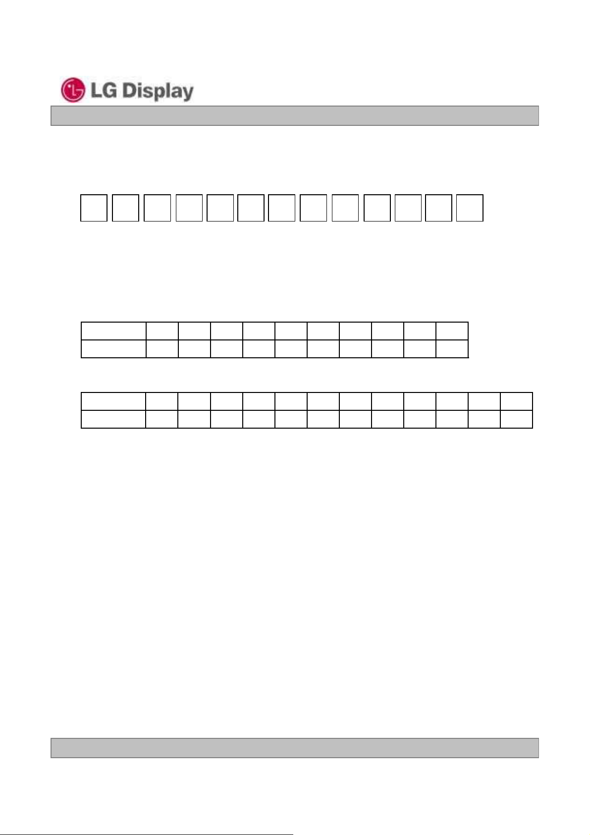
8-1. Designation of Lot Mark
a) Lot Mark
ABCDEFGHI JKLM
A,B,C : SIZE(INCH) D : YEAR
E : MONTH F ~ M : SERIAL NO.
Note
1. YEAR
LP173WF3
Liquid Crystal Display
Year
Mark
CBA
2014E2015
D
201320122011
2016G2017H2018J2019
F
2. MONTH
Month
Mark
Apr5May
4
Jun7Jul8Aug9Sep
6
b) Location of Lot Mark
Serial No. is printed on the label. The label is attached to the backside of the LCD module.
This is subject to change without prior notice.
8-2. Packing Form
a) Package quantity in one box : 20ea
b) Box Size : 480*380*280
2020
K
Oct
A
Nov
B
DecMarFebJan
C321
Ver. 1.1
Ver. 1.1
20. Oct. 2011
20. Oct. 2011
29 / 34
Page 30

LP173WF3
Liquid Crystal Display
Product Specification
9. PRECAUTIONS
Please pay attention to the followings when you use this TFT LCD module.
9-1. MOUNTING PRECAUTIONS
(1) You must mount a module using holes arranged in four corners or four sides.
(2) You should consider the mounting structure so that uneven force (ex. Twisted stress) is not applied to the
module. And the case on which a module is mounted s hould have sufficient strength so that external
force is not transmitted directly to the module.
(3) Please attach the surface transparent protective plate to the surface in order to protect the polarizer.
Transparent protective plate should have sufficient strength in order to the resist external force.
(4) You should adopt radiation structure to satisfy the temperature specification.
(5) Acetic acid type and chlorine type materials for the cover case are not des irable because the former
generates corrosive gas of attacking the polarizer at high temper ature and the latter causes cir cuit break
by electro-chemical reaction.
(6) Do not touch, push or rub the exposed polarizers with glass, tweezers or anything harder than HB
pencil lead. And please do not rub with dust clothes with chemical treatment.
Do not touch the surface of polarizer for bare hand or greasy cloth.(Some cosmetics are detrimental
to the polarizer.)
(7) When the surface becomes dusty, please wipe gently with absorbent cotton or other soft mater ials like
chamois soaks with petroleum benzene. Normal-hexane is recommended for cleaning the adhesives
used to attach front / rear polarizers. Do not use acetone, toluene and alcohol because they cause
chemical damage to the polarizer.
(8) Wipe off saliva or water drops as soon as possible. Their long time contact with polarizer causes
deformations and color fading.
(9) Do not open the case because inside circuits do not have sufficient strength.
9-2. OPERATING PRECAUTIONS
(1) The spike noise causes the mis-operation of circuits. It should be lower than following voltage :
V=± 200mV(Over and under shoot voltage)
(2) Response time depends on the temperature.(In lower temperature, it becomes longer.)
(3) Brightness depends on the temperature. (In lower temperature, it becomes lower.)
And in lower temperature, response time(required time tha t br ightness is stab le after tu rned on ) beco mes
longer.
(4) Be careful for condensation at sudden temperature change. Condensation makes damage to polarizer or
electrical contacted parts. And after fading condensation, smear or spot will occur.
(5) When fixed patterns are displayed for a long time, remnant image is likely to occur.
(6) Module has high frequency cir cuits. Sufficient suppression to the elec tromagnetic interference shall be
done by system manufacturers. Grounding and shielding methods may be important to minimized the
interference.
Ver. 1.1
Ver. 1.1
20. Oct. 2011
20. Oct. 2011
30 / 34
Page 31

LP173WF3
Liquid Crystal Display
Product Specification
9-3. ELECTROSTATIC DISCHARGE CONTROL
Since a module is composed of electronic circuits, it is not strong to elec trosta tic di scharge. Make cer tain that
treatment persons are connected to ground through wrist band etc. And don’t touch interface pin directly.
9-4. PRECAUTIONS FOR STRONG LIGHT EXPOSURE
Strong light exposure causes degradation of polarizer and color filter.
9-5. STORAGE
When storing modules as spares for a long time, the following precautions are necessary.
(1) Store them in a dark place. Do not expo se t h e mod ule to sunli g ht or flu oresce nt light. K ee p t he
temperature between 5C and 35C at normal humidity.
(2) The polarizer surface should not come in contact with any other object.
It is recommended that they be stored in the container in which they were shipped.
9-6. HANDLING PRECAUTIONS FOR PROTECTION FILM
(1) When the protection film is peeled off, static electricity is generated between the film and polarizer.
This should be peeled off slowly and carefully by people who are electrically grounded and with well
ion-blown equipment or in such a condition, etc.
(2) The protection film is attached to the polarizer with a small amount of glue. If some stress is applied
to rub the protection film against the polarizer during the time you peel off the film, the glue is apt to
remain on the polarizer.
Please carefully peel off the protection film without rubbing it against the polarizer.
(3) When the module with protection film attached is stored for a long time, sometimes there remains a
very small amount of glue still on the polarizer after the protection film is peeled off.
(4) You can remove the glue easily. When the glue remains on the polarizer surface or its vestige is
recognized, please wipe them off with absorbent cotton waste or other soft material like chamois
soaked with normal-hexane.
Ver. 1.1
Ver. 1.1
20. Oct. 2011
20. Oct. 2011
31 / 34
Page 32
Liquid Crystal Display
g
d
Product Specification
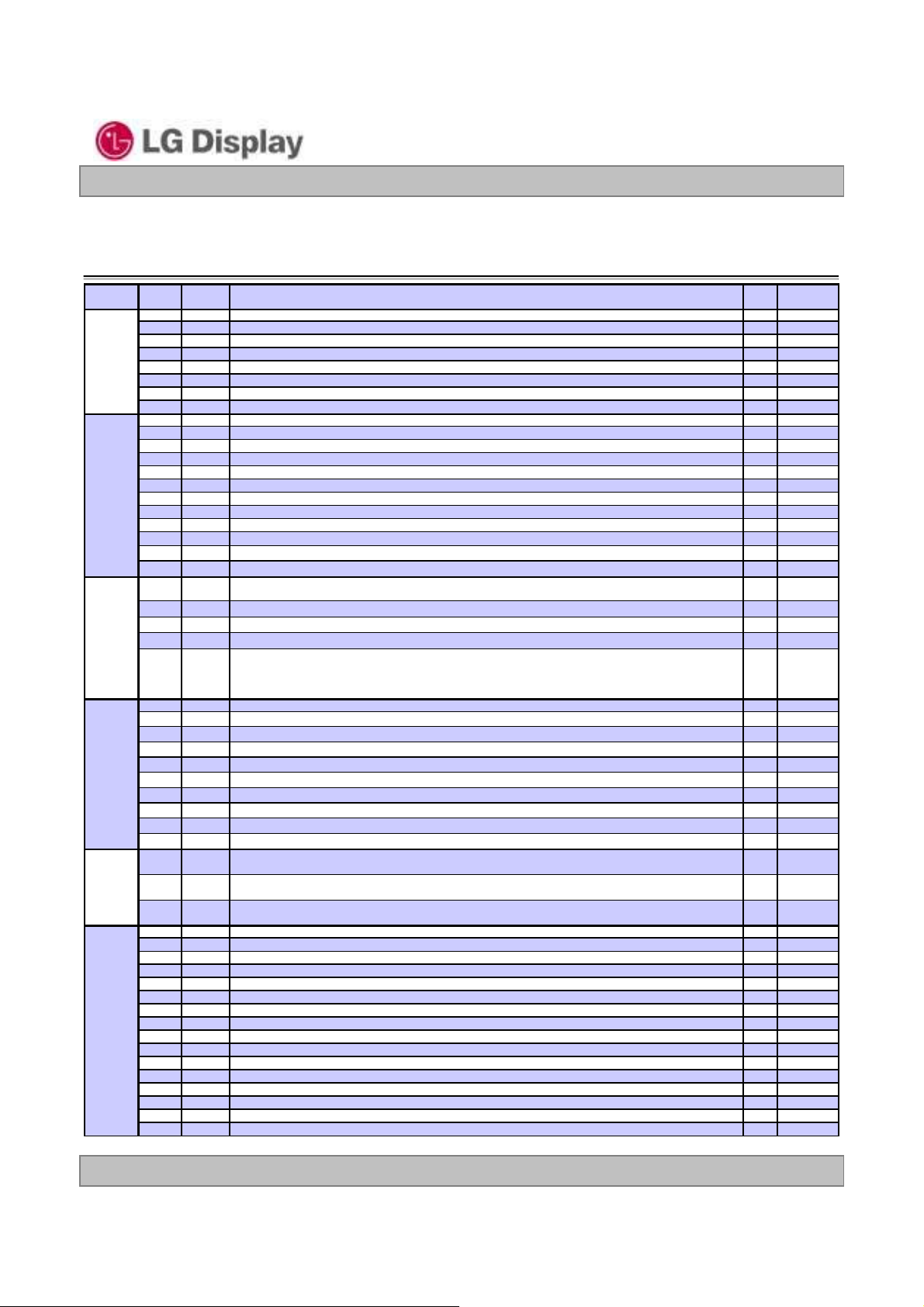
APPENDIX A. Enhanced Extended Display Identification Data (EEDIDTM) 1/3
LP173WF3
EDID Data for
Byte
(Dec)
Header
ED ID Version
Vendor / Product
Display P a ra metersPanel Color Coordinates
Timings
Esta b lish e d
Standard Timing ID
Byte
(Hex)
0
1
2
3
4
5
6
7
8
9
10
11
12
13
14
15
16
17
18
19
20
21
22
23
24
25
26
27
28
29
30
31
32
33
34
35
36
37
38
39
40
41
42
43
44
45
46
47
48
49
50
51
52
53
Header
00
Header
01
Header
02
Header
03
Header
04
Header
05
Header
06
Header
07
ID Manufacture Name LGD
08
ID Manufacture Name
09
ID Product Code 02FCh
0A
( Hex. LSB first )
0B
ID Serial No. - Op t i on a l ( "0 0h" If not used, Num ber Only and LSB First)
0C
ID Serial No. - Op t i on a l ( "0 0h" If not used, Num ber Only and LSB First)
0D
ID Serial No. - Op t i on a l ( "0 0h" If not used, Num ber Only and LSB First)
0E
ID Serial No. - Op t i on a l ( "0 0h" If not used, Num ber Only and LSB First)
0F
Week of Manufacture - Optinal 00 weeks
10
Year of Manufacture 2010 years
11
EDID structure version # = 1
12
EDID revision # = 4
13
Video input Definition = Input is a Digital Video signal Interface , Colo Bit Depth : 10 Bits per Primary Color ,
14
Di
ital Video Interface Standard Supported: Digital Interface is not define
Horizontal Screen Size ( Roun ded cm ) = 3 8 cm 3 8 cm
15
Vertical Screen Size ( Rounded cm) = 21 cm21 cm
16
Display Transfer Characteristic (Gamma) = (gamma*100)-100 = Example:(2.2*100)-100=120 = 2 . 2 Ga mm a
17
Feature Support [ Display Power Management(DPM) : Standby Mode is not supported, Suspend Mode is not
supported, Active Off = Very Low Power is not supported ,Supportted Color Encoding Forma ts : RGB 4:4:4 &
18
YCrCb 4:4:4 ,Other Feature Support Flags : No_sRGB, Preferred Timing Mode, No_Display is continuous
frequency (Multi-mode_Base EDID and Extension Block).]
Red/Green Low Bits (RxRy/GxGy)
19
Blue/White Low Bits (BxBy/WxWy)
1A
Red X Rx = 0.686
1B
Red Y Ry = 0.308
1C
Green X Gx = 0.213
1D
Green Y Gy = 0.715
1E
Blue X Bx = 0.145
1F
Blue Y By = 0.045
20
White X Wx = 0.313
21
White Y Wy = 0.329
22
Established timing 1 ( Optional_00h if not used)
23
Established timing 2 ( Optional_00h if not used)
24
Manufacturer's timin g s ( Optiona l_00h if not used)
25
Standard timing ID1 ( Optional_01h if not used)
26
Standard timing ID1 ( Optional_01h if not used)
27
Standard timing ID2 ( Optional_01h if not used)
28
Standard timing ID2 ( Optional_01h if not used)
29
Standard timing ID3 ( Optional_01h if not used)
2A
Standard timing ID3 ( Optional_01h if not used)
2B
Standard timing ID4 ( Optional_01h if not used)
2C
Standard timing ID4 ( Optional_01h if not used)
2D
Standard timing ID5 ( Optional_01h if not used)
2E
Standard timing ID5 ( Optional_01h if not used)
2F
Standard timing ID6 ( Optional_01h if not used)
30
Standard timing ID6 ( Optional_01h if not used)
31
Standard timing ID7 ( Optional_01h if not used)
32
Standard timing ID7 ( Optional_01h if not used)
33
Standard timing ID8 ( Optional_01h if not used)
34
Standard timing ID8 ( Optional_01h if not used)
35
Field Name an d Co mment s
HP Dream Color _
ver. 0.0
Value
(Hex)
00
FF
FF
FF
FF
FF
FF
00
30
E4
FC
02
00
00
00
00
00
14
01
04
B0
26
15
78
0A
B8
25
AF
4E
36
B7
25
0B
50
54
00
00
00
01
01
01
01
01
01
01
01
01
01
01
01
01
01
01
01
2010/10/27
Value
(Bin)
00000000
11111111
11111111
11111111
11111111
11111111
11111111
00000000
00110000
11100100
11111100
00000010
00000000
00000000
00000000
00000000
00000000
00010100
00000001
00000100
10110000
00100110
00010101
01111000
00001010
10111000
00100101
10101111
01001110
00110110
10110111
00100101
00001011
01010000
01010100
00000000
00000000
00000000
00000001
00000001
00000001
00000001
00000001
00000001
00000001
00000001
00000001
00000001
00000001
00000001
00000001
00000001
00000001
00000001
Ver. 1.1
Ver. 1.1
20. Oct. 2011
20. Oct. 2011
32 / 34
Page 33
Liquid Crystal Display
@
Product Specification
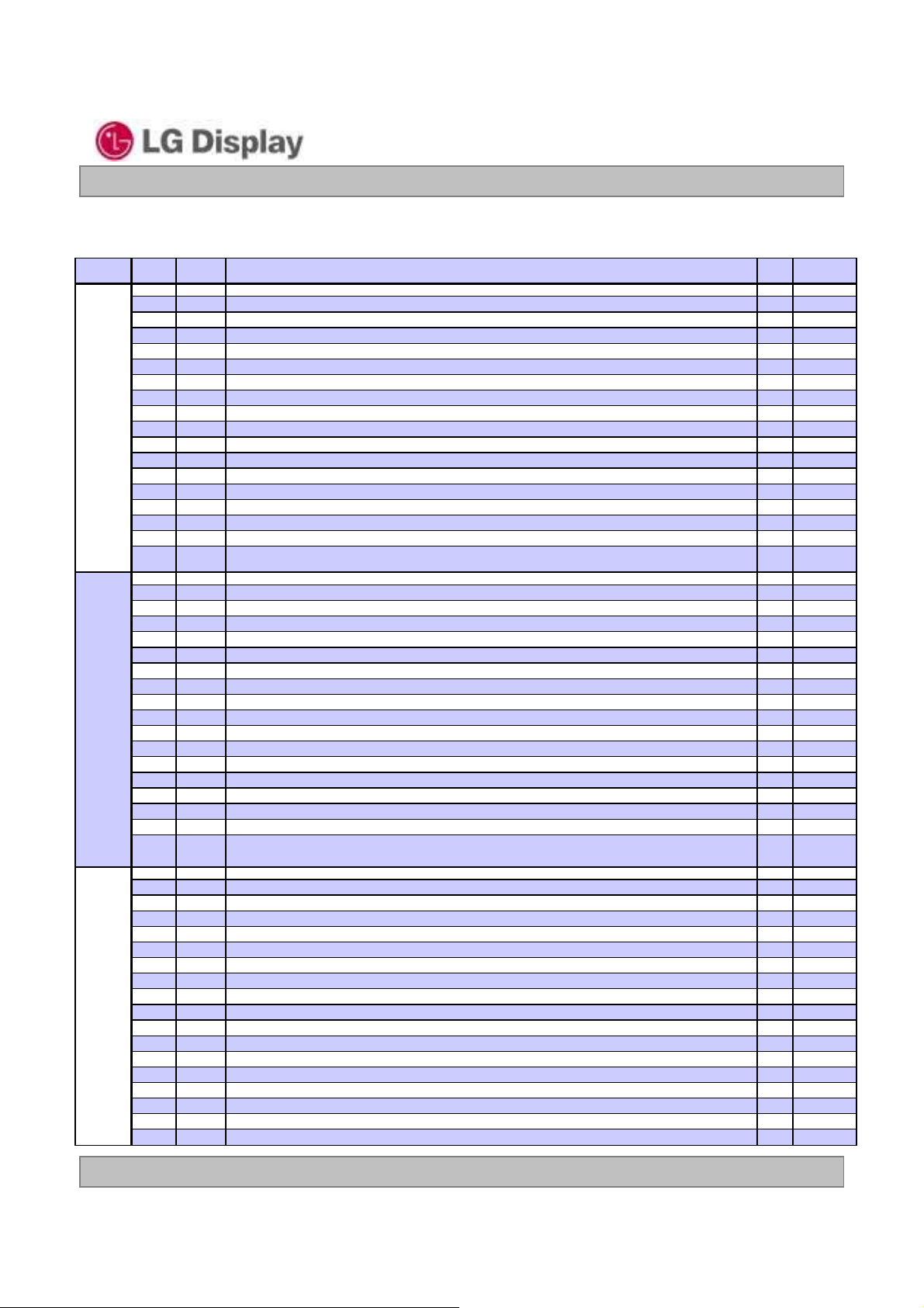
APPENDIX A. Enhanced Extended Display Identification Data (EEDIDTM) 2/3
LP173WF3
Byte
(Dec)
Timing Descriptor #3 Timing Descriptor #1Timing Descriptor #2
54
55
56
57
58
59
60
61
62
63
64
65
66
67
68
69
70
71
72
73
74
75
76
77
78
79
80
81
82
83
84
85
86
87
88
89
90
91
92
93
94
95
96
97
98
99
100
101
102
103
104
105
106
107
Byte
(He x)
Pixel Clock /10,0 00 (L SB ) 138.7 MHz
36
Pixel Clock/10,000 (MSB)
37
Horizon tal A ctive (lower 8 bits) 1920 Pixels
38
Horizon tal Bla n kin g(T h p-H A ) (lower 8 bits) 160 P ixels
39
Horizontal Active / Horizontal Blanking(Thp-HA) (upper 4:4bits)
3A
Vertical A vtive 1080 Lines
3B
Vertical Bla n kin g (T vp-H A ) (DE B lan kin g typ.for D E only pa n els) 31 Lines
3C
Vertical Active : Vertical Blanking (Tvp-HA) (upper 4:4bits)
3D
Horizon tal Syn c. Offset (Th fp) 48 Pixels
3E
Horizon tal Syn c Pulse Width (HS PW) 32 Pixels
3F
Vertical Syn c O ffset(Tvfp) : Sync W idth (V SP W ) 3 Lines : 5 Lin es
40
Horizon tal V ertical S ync O ffset/Width (upp er 2bits)
41
Horizon tal Im a ge Siz e (m m ) 382 mm
42
Vertical Im a ge S ize (m m ) 215 mm
43
Horizontal Image Size / Vertical Image Size
44
Horizontal Border = 0 (Zero for Notebook LCD)
45
Vertical Border = 0 (Zero for Notebook LCD)
46
Non-Interlace, Normal display, no stereo, Digital Separate [ Vsync_NEG, Hsync_NEG (outside of V-sync) ]
47
Pixel Clock /10,0 00 (L SB ) 110.96 MH z @ 48 Hz
48
Pixel Clock/10,000 (MSB)
49
Horizon tal A ctive (lower 8 bits) 1920 Pixels
4A
Horizon tal Bla n kin g(T h p-H A ) (lower 8 bits) 160 P ixels
4B
Horizontal Active / Horizontal Blanking(Thp-HA) (upper 4:4bits)
4C
Vertical A vtive 1080 Lines
4D
Vertical Bla n kin g (T vp-H A ) (DE B lan kin g typ.for D E only pa n els) 31 Lines
4E
Vertical Active : Vertical Blanking (Tvp-HA) (upper 4:4bits)
4F
Horizon tal Syn c. Offset (Th fp) 48 Pixels
50
Horizon tal Syn c Pulse Width (HS PW) 32 Pixels
51
Vertical Syn c O ffset(Tvfp) : Sync W idth (V SP W ) 3 Lines : 5 Lin es
52
Horizon tal V ertical S ync O ffset/Width (upp er 2bits)
53
Horizon tal Im a ge Siz e (m m ) 382 mm
54
Vertical Im a ge S ize (m m ) 215 mm
55
Horizontal Image Size / Vertical Image Size
56
Horizontal Border = 0 (Zero for Notebook LCD)
57
Vertical Border = 0 (Zero for Notebook LCD)
58
Non-Interlace, Normal display, no stereo, Digital Separate [ Vsync_NEG, Hsync_NEG (outside of V-sync) ]
59
Maximum DCLK (T-CON to Driver IC) Integer Part 144.25 M Hz
5A
Maximum DCLK (T-CON to Driver IC) Fractional Part
5B
Min im u m D C LK (T -C ON to D river IC) In teger Pa rt 133.15 M Hz
5C
Minimum DCLK (T-CON to Driver IC) Fractional Part
5D
Hblank M a xim u m Settin g (H igh byte) 248 Pixels
5E
Hblank M ax im u m Settin g (L ow Byte)
5F
Hblank M in im u m Settin g (H igh byte) 80 Pixels
60
Hblank M in im um Settin g (L ow Byte)
61
Vblan k M a ximum Settin g (Hig h byte) 31 Pixels (Typical)
62
Vblan k M a ximum Settin g (Low Byte)
63
Vblan k M in imum Settin g (Hig h byte) 31 Pixels (Typical)
64
Vblan k M in imum S etting (Low B yte)
65
Type of bus between T -C ON a n d D river IC M ini-L VD S
66
DCL K M ultip lier/D ivider In teger between T -CO N an d D river IC 1.00 T im es
67
DCL K M ultip lier/D ivider F raction al between T -C O N an d D river IC
68
Spread Spectr um Settin g between T -C on a n d D river IC SS Disabled
69
Flags
6A
Flags
6B
Field Name and Comments
60Hz
Value
(Hex)
2E
36
80
A0
70
38
1F
40
30
20
35
00
7E
D7
10
00
00
19
58
2B
80
A0
70
38
1F
40
30
20
35
00
7E
D7
10
00
00
19
90
19
85
0F
00
F8
00
50
00
1F
00
1F
01
01
00
00
00
00
Value
(Bin)
00101110
00110110
10000000
10100000
01110000
00111000
00011111
01000000
00110000
00100000
00110101
00000000
01111110
11010111
00010000
00000000
00000000
00011001
01011000
00101011
10000000
10100000
01110000
00111000
00011111
01000000
00110000
00100000
00110101
00000000
01111110
11010111
00010000
00000000
00000000
00011001
10010000
00011001
10000101
00001111
00000000
11111000
00000000
01010000
00000000
00011111
00000000
00011111
00000001
00000001
00000000
00000000
00000000
00000000
Ver. 1.1
Ver. 1.1
20. Oct. 2011
20. Oct. 2011
33 / 34
Page 34
Liquid Crystal Display
Product Specification
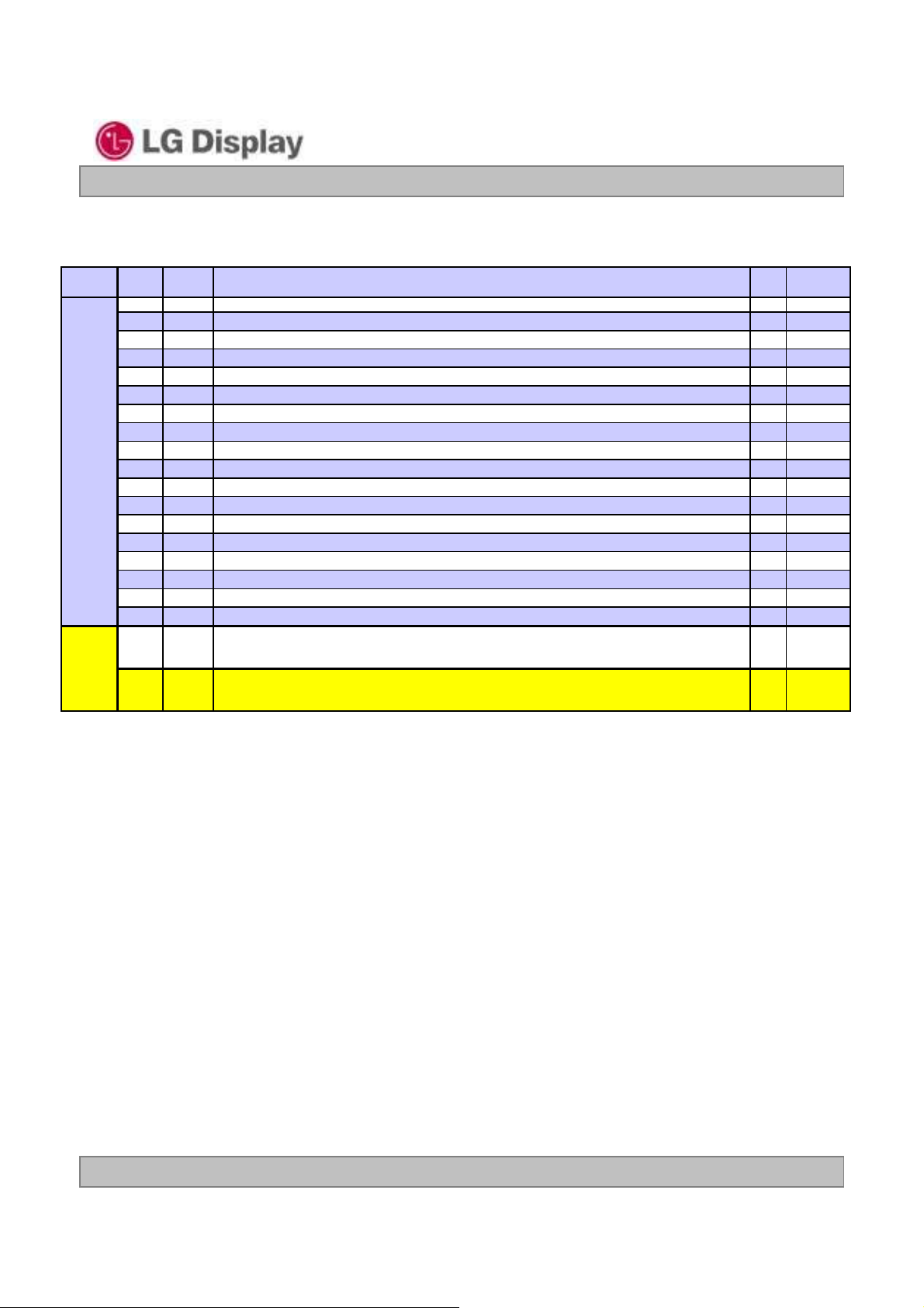
APPENDIX A. Enhanced Extended Display Identification Data (EEDIDTM) 3/3
LP173WF3
Timing Descriptor #4Checksum
Byte
(Dec)
108
109
110
111
112
113
114
115
116
117
118
119
120
121
122
123
124
125
126
127
Byte
(Hex)
Pixel Clock/10,000 (LSB) 115.58 MHz @ 50Hz
6C
Pixel Clock/10,000 (MSB)
6D
Horizontal Active (lower 8 bits) 1920 Pixels
6E
Horizontal Blanking(Thp-HA) (lower 8 bits) 160 Pixels
6F
Horizontal Active / Horizontal Blan ki ng(Thp-HA) (upper 4:4bits)
70
Vertical Avtive 1080 Lines
71
Vertical Blanking (Tvp-HA) (DE Blanking typ.for DE only panels) 31 Lines
72
Vertical Active : Vertical Blanking (Tvp-HA) (upper 4:4bits)
73
Horizontal Sync. Offset (Thfp) 48 Pixels
74
Horizontal Sync Pulse Width (HSPW) 32 Pixels
75
Vertical Sync Offset(Tvfp) : Sync Width (VSPW) 3 Lines : 5 Lines
76
Horizontal Vertical Sync Offset/Width (upper 2bits)
77
Horizontal Image Size (mm) 382 mm
78
Vertical Image Size (mm) 215 mm
79
Horizontal Image Size / Vertical Image Size
7A
Horizont al Bor der = 0 (Zero for Notebook LCD )
7B
Vertical Borde r = 0 (Zero for Note book LCD)
7C
Non-Interlace, Norma l d i sp l a y, n o stereo, Digital Separat e [ Vsync_NE G, Hsync_NEG (outside of V-sync) ]
7D
Extension flag (# of optional 128 panel ID extension block to follow, Typ = 0)
7E
Check Sum (The 1-byte sum of all 128 bytes in this panel ID block shall = 0)
7F
Field Name and Co mments
Value
(Hex)
26
2D
80
A0
70
38
1F
40
30
20
35
00
7E
D7
10
00
00
19
00
46
Value
(Bin)
00100110
00101101
10000000
10100000
01110000
00111000
00011111
01000000
00110000
00100000
00110101
00000000
01111110
11010111
00010000
00000000
00000000
00011001
00000000
01000110
Ver. 1.1
Ver. 1.1
20. Oct. 2011
20. Oct. 2011
34 / 34
 Loading...