

Page 1
Global LCD Panel Exchange Center
www.panelook.com
LP173WD1
Liquid Crystal Display
Product Specification
SPECIFICATION
FOR
APPROVAL
)
(
(
Preliminary Specification
)
Final Specification
17.3” HD+ TFT LCDTitle
LG Display Co., Ltd.SUPPLIER
LP173WD1*MODEL
TLD3Suffix
MODEL
APPROVED BY
/
/
HPBUYER
*When you obtain standard approval,
please use the above model name without suffix
APPROVED BY SIGNATURE
SIGNATURE
K. J. KWON / S.Manager
REVIEWED BY
G. J. Han / Manager
PREPARED BY
/
Please return 1 copy for your confirmation with
your signature and comments.
Ver. 0.0 18. Sep, 2009
H. M. Yoon / Engineer
H. J. Kim / Engineer
Product Engineering Dept.
LG Display Co., Ltd
One step solution for LCD / PDP / OLED panel application: Datasheet, inventory and accessory!
1/ 31
www.panelook.com
Page 2
Global LCD Panel Exchange Center
www.panelook.com
LP173WD1
Liquid Crystal Display
Product Specification
Contents
COVER
CONTENTS
RECORD OF REVISIONS
GENERAL DESCRIPTION1
ABSOLUTE MAXIMUM RATINGS2
ELECTRICAL SPECIFICATIONS3
ELECTRICAL CHARACTREISTICS3-1
INTERFACE CONNECTIONS3-2
LVDS SIGNAL TIMING SPECIFICATIONS3-3
SIGNAL TIMING SPECIFICATIONS3-4
SIGNAL TIMING WAVEFORMS3-5
COLOR INPUT DATA REFERNECE3-6
POWER SEQUENCE3-7
OPTICAL SFECIFICATIONS4
ITEMNo
Page
1
2
3
4
5
6
8
10
10
11
12
12
MECHANICAL CHARACTERISTICS5
RELIABLITY6
INTERNATIONAL STANDARDS7
SAFETY7-1
EMC7-2
PACKING8
DESIGNATION OF LOT MARK8-1
PACKING FORM8-2
PRECAUTIONS9
APPENDIX A. Enhanced Extended Display Identification DataA
Ver. 0.0 18. Sep, 2009
16
23
24
24
25
25
26
28
2/ 31
One step solution for LCD / PDP / OLED panel application: Datasheet, inventory and accessory!
www.panelook.com
Page 3
Global LCD Panel Exchange Center
www.panelook.com
LP173WD1
Liquid Crystal Display
Product Specification
RECORD OF REVISIONS
DescriptionPageRevision DateRevision No
EDID
ver
0.0First Draft-Sep. 18. 20090.0
Ver. 0.0 18. Sep, 2009
One step solution for LCD / PDP / OLED panel application: Datasheet, inventory and accessory!
3/ 31
www.panelook.com
Page 4
Global LCD Panel Exchange Center
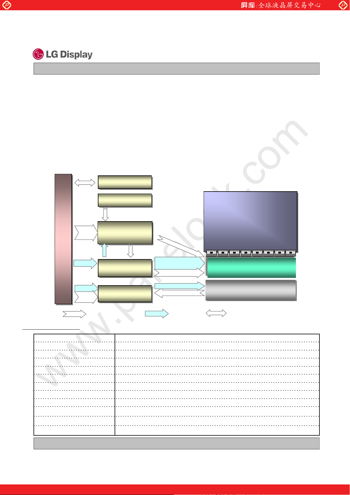
1. General Description
The LP173WD1 is a Color Active Matrix Liquid Crystal Display with an integral LED backlight system. The
matrix employs a-Si Thin Film Transistor as the active element. It is a transmissive type display operating in
the normally white mode. This TFT-LCD has 17.3 inches diagonally measured active display area with
WHD+ resolution(1600 horizontal by 900 vertical pixel array). Each pixel is divided into Red, Green and
Blue sub-pixels or dots which are arranged in vertical stripes. Gray scale or the brightness of the sub-pixel
color is determined with a 6-bit gray scale signal for each dot, thus, presenting a palette of more than
262,144 colors. The LP173WD1 has been designed to apply the interface method that enables low power,
high speed, low EMI. The LP173WD1 is intended to support applications where thin thickness, low power
are critical factors and graphic displays are important. In combination with the vertical arrangement of the
sub-pixels, the LP173WD1 characteristics provide an excellent flat display for office automation products
such as Notebook PC.
www.panelook.com
LP173WD1
Liquid Crystal Display
Product Specification
User connector
40
Pin
General Features
EEPROM Block
EEPROM Block
for EDID
for EDID
EEPROM Block
EEPROM Block
for Tcon Operating
for Tcon Operating
Timing Control
LVDS
2port
VCC
VLED
LED_EN
PWM
Timing Control
(Tcon) Block
(Tcon) Block
DVCC
Power
Block
LED Driver
LED Driver
Block
TCLKs
Power
Block
Block
VGH, VGL, GMA
Control & Data Power
17.3 inches diagonal Active Screen Size
398.1(H, Typ.) Ý 232.8(V, Typ.) Ý 6.0(D, Max.) mmOutline Dimension
0.23868 X 0.23868 mmPixel Pitch
1600 horiz. by 900 vert. Pixels RGB strip arrangementPixel Format
6-bit, 262,144 colorsColor Depth
200 cd/m
Logic : 1.5 W (Typ.@Mosaic), Back Light : 5.0W (Typ.)Power Consumption
570g (Max.)Weight
Transmissive mode, normally whiteDisplay Operating Mode
Anti-Glare treatment of the front Polarizer Surface Treatment
YesRoHS Comply
Yes all. BFR / PVC / As Free
2
(Typ., @I
M
i
n
i
-
L
V
D
S
AVCC, AVDD
GIP CLKs, DSC
VOUT_LED
FB1~6
=21mA)Luminance, White
LED
1
900
1600
TFT-LCD Panel
(HD, GIP, TN)
Source Driver
(Bottom Bent)
LED Backlight Ass’y
EDID signal & Power
Ver. 0.0 18. Sep, 2009
One step solution for LCD / PDP / OLED panel application: Datasheet, inventory and accessory!
4/ 31
www.panelook.com
Page 5
Global LCD Panel Exchange Center
2. Absolute Maximum Ratings
The following are maximum values which, if exceeded, may cause faulty operation or damage to the unit.
www.panelook.com
LP173WD1
Liquid Crystal Display
Product Specification
Table 1. ABSOLUTE MAXIMUM RATINGS
Parameter Notes
Symbol
Values
MaxMin
Units
Power Input Voltage
Operating Temperature
Storage Temperature
Operating Ambient Humidity
OP
Storage Humidity
Note : 1. Temperature and relative humidity range are shown in the figure below.
Wet bulb temperature should be 39
Wet Bulb
Temperature [
10
0
20
]
30
qC Max, and no condensation of water.
90% 80%
60
50
40
60%
Humidity[(%)RH]
40%
20%
10%
Storage
Operation
at 25 r 5qCVdc4.0-0.3VCC
1qC500TOP
1qC60-20HST
1%RH9010H
1%RH9010HST
-20
10
20 30 40 50
60 70 800
Dry Bulb Temperature []
Ver. 0.0 18. Sep, 2009
One step solution for LCD / PDP / OLED panel application: Datasheet, inventory and accessory!
5/ 31
www.panelook.com
Page 6
Global LCD Panel Exchange Center
3. Electrical Specifications
3-1. Electrical Characteristics
The LP173WD1 requires two power inputs. The first logic is employed to power the LCD electronics and to
drive the TFT array and liquid crystal. The second backlight is the input about LED BL with LED Driver.
www.panelook.com
LP173WD1
Liquid Crystal Display
Product Specification
Table 2. ELECTRICAL CHARACTERISTICS
LOGIC :
Power Supply Input Current
BACKLIGHT : ( with LED Driver)
PWM Jitter
Values
SymbolParameter
NotesUnit
MaxTypMin
CCPower Supply Input Voltage
CCMosaic
CC_maxBlack
CCPower Consumption
CC_PPower Supply Inrush Current
LVDSLVDS Impedance
LEDLED Power Input Voltage
LEDLED Power Input Current
LEDLED Power Consumption
LED_PLED Power Inrush Current
11010090Z
ȳ
1V3.63.33.0V
2mA515455-I
3mA660575-I
2W1.71.5-P
4mA18001200-I
5
6V20.012.07.0V
7mA2521-I
7W5.35.0-P
8mA1000800-I
9%100-6PWM Duty Ratio
-
10%0.2-0
PWMPWM Impedance
PWMPWM Frequency
PWM High Level Voltage
PWM Low Level Voltage
LED_EN High Voltage
LED_EN Low Voltage
Ver. 0.0 18. Sep, 2009
PWM_H
PWM_L
PWMLED_EN Impedance
V
LED_EN
LED_EN
V
_H
_L
One step solution for LCD / PDP / OLED panel application: Datasheet, inventory and accessory!
kȳ604020Z
11Hz1000-200F
V5.3-3.0V
V0.5-0V
kȳ604020Z
V5.3-3.0
V0.5-0
12Hrs--12,000Life Time
6/ 31
www.panelook.com
Page 7
Global LCD Panel Exchange Center
Note)
1. The measuring position is the connector of LCM and the test conditions are under 25, fv = 60Hz,
Black pattern.
2. The specified Icc current and power consumption are under
the Vcc = 3.3V , 25, fv = 60Hz condition whereas Mosaic pattern
is displayed and fv is the frame frequency.
3. This Spec. is the max load condition for the cable impedance designing.
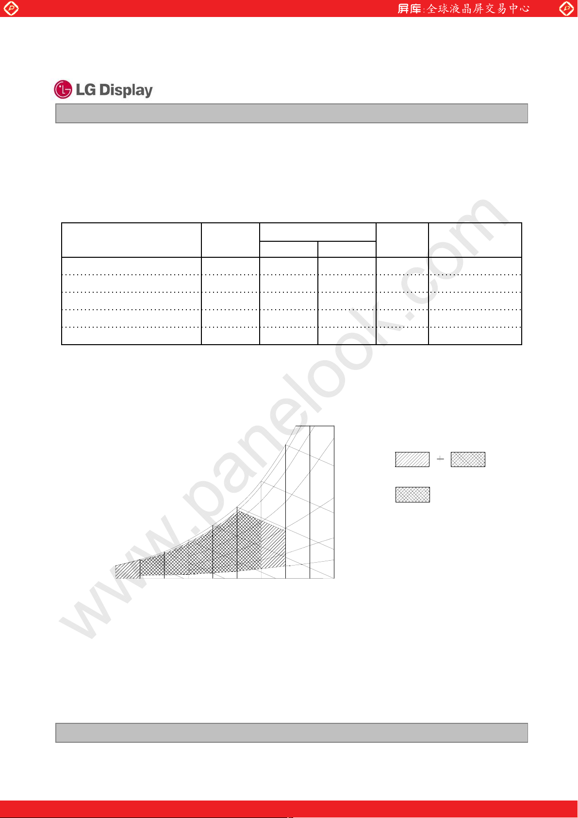
4. The below figures are the measuring Vcc condition and the Vcc control block LGD used.
The Vcc condition is same the minimum of T1 at Power on sequence.
www.panelook.com
LP173WD1
Liquid Crystal Display
Product Specification
Rising time
Vcc
0V
5. This impedance value is needed to proper display and measured form LVDS Tx to the mating connector.
6. The measuring position is the connector of LCM and the test conditions are under 25.
7. The current and power consumption with LED Driver are under the Vled = 12.0V , 25, Dimming of
Max luminance whereas White pattern is displayed and fv is the frame frequency.
8. The below figures are the measuring Vled condition
and the Vled control block LGD used.
VLED control block is same with Vcc control block.
90%
10%
0.5ms
3.3V
Rising time
LED
V
0V
10%
12.0V
90%
0.5ms
9. The operation of LED Driver below minimum dimming ratio may cause flickering or reliability issue.
10. If Jitter of PWM is bigger than maximum. It may cause flickering.
11. This Spec. is not effective at 100% dimming ratio as an exception because it has DC level equivalent
to 0Hz. In spite of acceptable range as defined, the PWM Frequency should be fixed and stable for
more consistent brightness control at any specific level desired.
12 The life time is determined as the time at which the typical brightness of LCD is 50% compare to that of
initial value at the typical LED current. These LED backlight has 6 strings on it and the typical current
of LED’s string is base on 21mA.
Ver. 0.0 18. Sep, 2009
One step solution for LCD / PDP / OLED panel application: Datasheet, inventory and accessory!
7/ 31
www.panelook.com
Page 8
Global LCD Panel Exchange Center
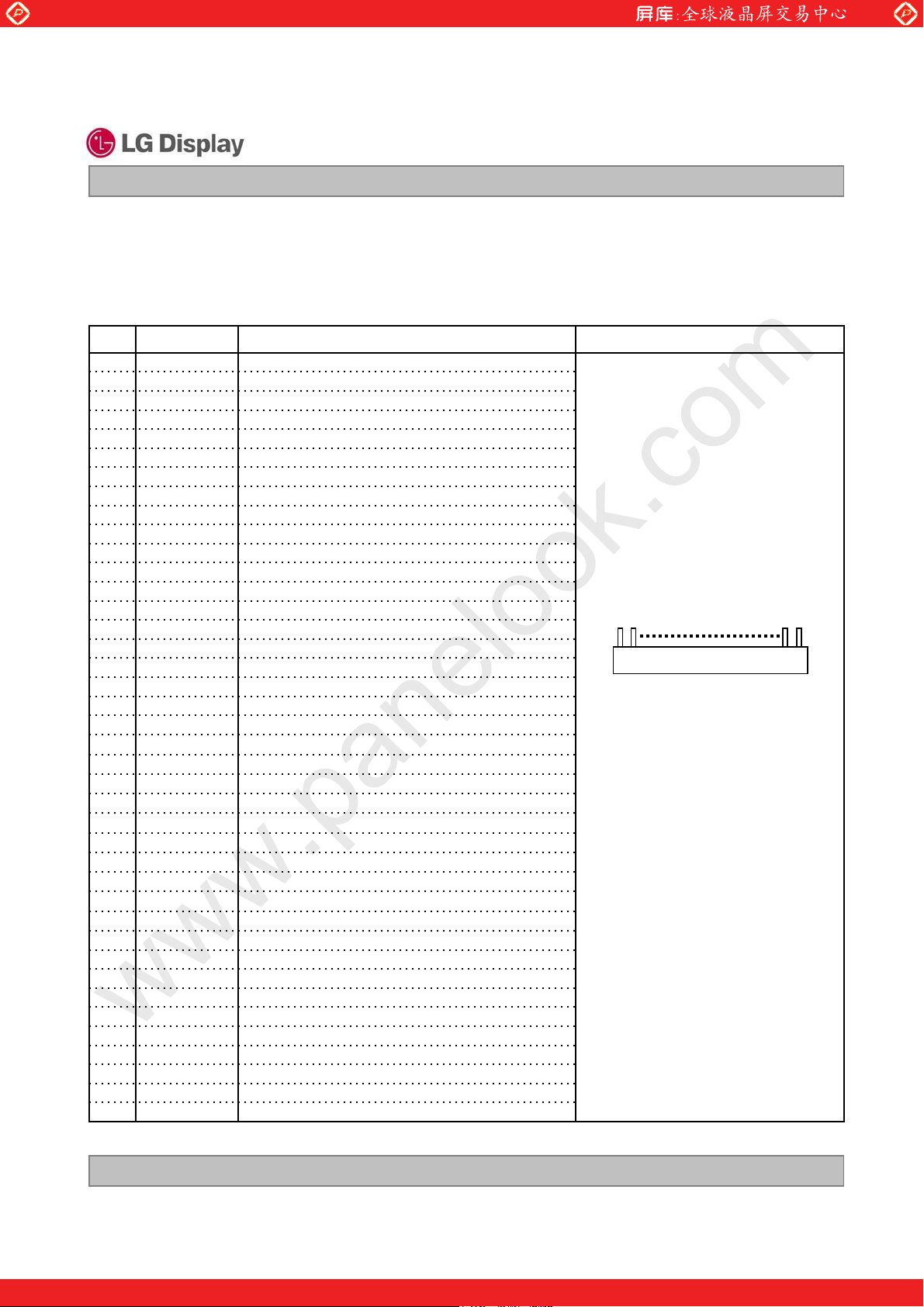
3-2. Interface Connections
This LCD employs two interface connections, a 40 pin connector is used for the module electronics interface
and the other connector is used for the integral backlight system.
The electronics interface connector is a model CABLINE-VS RECE ASS’Y manufactured by I-PEX.
Table 3. MODULE CONNECTOR PIN CONFIGURATION (CN1)
No ConnectionNC1
Power Supply, 3.3V Typ.VCC2
Power Supply, 3.3V Typ.VCC3
DDC 3.3V powerV EEDID4
No ConnectionNC5
DDC ClockClk EEDID6
DDC DataDATA EEDID7
Negative LVDS differential data inputOdd_R
0-8
IN
0+9
Positive LVDS differential data inputOdd_R
GroundGND10
1-11
Negative LVDS differential data inputOdd_R
IN
Positive LVDS differential data inputOdd_R
1+12
GroundGND13
Negative LVDS differential data inputOdd_R
2-14
IN
Positive LVDS differential data inputOdd_R
2+15
GroundGND16
Negative LVDS differential clock inputOdd_CLKIN-17
Positive LVDS differential clock inputOdd_CLKIN+18
GroundGND19
0-20
1HJDWLYH/9'6GLIIHUHQWLDOGDWDLQSXW55*
IN
3RVLWLYH/9'6GLIIHUHQWLDOGDWDLQSXW55*
*URXQG
1-23
1HJDWLYH/9'6GLIIHUHQWLDOGDWDLQSXW**%%
IN
1+24
3RVLWLYH/9'6GLIIHUHQWLDOGDWDLQSXW**%%
IN
*URXQG
1HJDWLYH/9'6GLIIHUHQWLDOGDWDLQSXW%
2-26
IN
%+696'(
3RVLWLYH/9'6GLIIHUHQWLDOGDWDLQSXW%
2+27
IN
%+696'(
*URXQG
1HJDWLYH/9'6GLIIHUHQWLDOFORFNLQSXW
3RVLWLYH/9'6GLIIHUHQWLDOFORFNLQSXW
LED Ground
LED GroundGND
LED GroundGND
No ConnectionNC
PWM for luminance control(200Hz ~ 1000Hz)PWM
Backlight On/Off ControlLED_EN
No Connection (Reserved)NC
LED Power Supply (7V-21V)VLED
LED Power Supply (7V-21V)VLED
LED Power Supply (7V-21V)VLED
21
32
33
34
35
36
37
38
39
40
IN
IN
IN
Even_R
Even_RIN0+
GND19
Even_R
Even_R
GND19
Even_R
Even_R
GND19
Even_CLKIN-29
Even_CLKIN+30
GND31
www.panelook.com
Product Specification
LP173WD1
Liquid Crystal Display
NotesDescriptionSymbolPin
1, Interface chips
1.1 LCD : SW, SW0617 (LCD Controller)
including LVDS Receiver
1.2 System : THC63LVDF823A
* Pin to Pin compatible with LVDS
2. Connector
2.1 LCD : CABLINE-VS RECE ASS’Y, I-PEX
2.2 Mating : CABLINE-VS PLUG CABLE
2.3 Connector pin arrangement
or equivalent
or its compatibles
ASS’Y or equivalent.
[LCD Module Rear View]
Ver. 0.0 18. Sep, 2009
One step solution for LCD / PDP / OLED panel application: Datasheet, inventory and accessory!
8/ 31
www.panelook.com
Page 9
Global LCD Panel Exchange Center
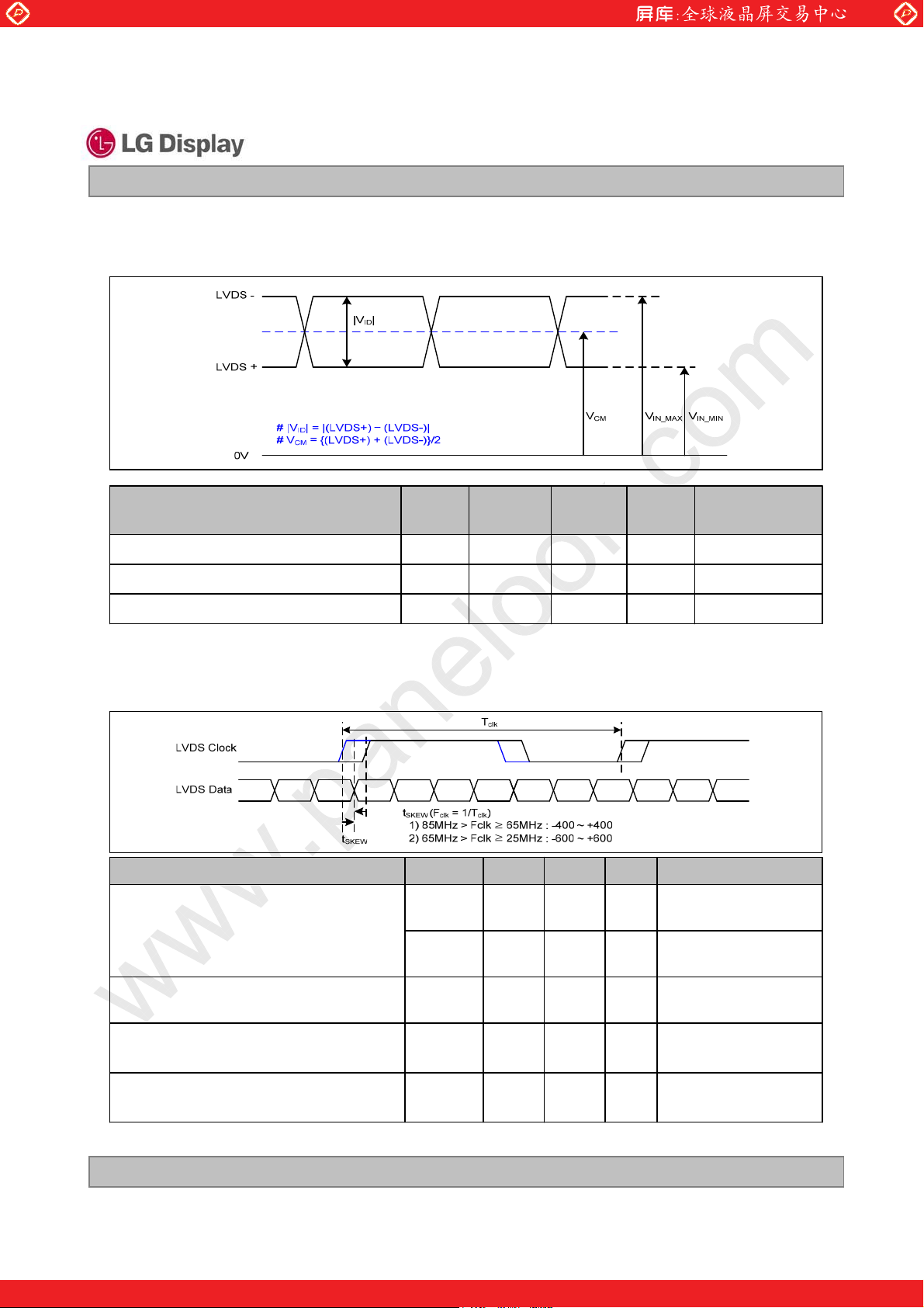
3-3. LVDS Signal Timing Specifications
3-3-1. DC Specification
www.panelook.com
LP173WD1
Liquid Crystal Display
Product Specification
Description
LVDS Common mode Voltage
LVDS Input Voltage Range
3-3-2. AC Specification
LVDS Clock to Data Skew Margin
Symb
ol
ID
CM
IN
SKEW
SKEW
NotesUnitMaxMin
|LVDS Differential Voltage
-mV600100|V
-V1.80.6V
-V2.10.3V
NotesUnitMaxMinSymbolDescription
85MHz > Fclk ˻
65MHz
65MHz > Fclk ˻
25MHz
- 600
ps+ 400- 400t
ps+ 600t
LVDS Clock to Clock Skew Margin (Even
to Odd)
SKEW_EO
Maximum deviation
of input clock frequency during SSC
DEV
Maximum modulation frequency
of input clock during SSC
Ver. 0.0 18. Sep, 2009
MOD
-1/7
+ 1/7t
T
clk
%· 3-F
KHz200-F
One step solution for LCD / PDP / OLED panel application: Datasheet, inventory and accessory!
-
-
-
9/ 31
www.panelook.com
Page 10
Global LCD Panel Exchange Center
Freq.
www.panelook.com
LP173WD1
Liquid Crystal Display
Product Specification
< Clock skew margin between channel >
F
max
F
center
F
min
3-3-3. Data Format
1) LVDS 2 Port
X
m
tvk
< Spread Spectrum >
m
QGm
Time
kl}
< LVDS Data Format >
Ver. 0.0 18. Sep, 2009
One step solution for LCD / PDP / OLED panel application: Datasheet, inventory and accessory!
10/ 31
www.panelook.com
Page 11

Global LCD Panel Exchange Center
࣪࣪࣪
3-4. Signal Timing Specifications
This is the signal timing required at the input of the User connector. All of the interface signal timing should be
satisfied with the following specifications and specifications of LVDS Tx/Rx for its proper operation.
www.panelook.com
LP173WD1
Liquid Crystal Display
Product Specification
Table 5. TIMING TABLE
ࣿ
Period
Width
Width-Active
Period
Width
Width-Active
Horizontal back porch
Horizontal front porch
Vertical back porch
Vertical front porch
3-5. Signal Timing Waveforms
ࣿࣜ
ࣽ
ࣽ
HBP
ࣾ
High: 0.7VCC
Low: 0.3VCC
ࣰࣰࣱࣱࣱࣱ࣯࣯࣬࣪ࣳࣴ࣪ࣴࣳࣳ࣪ࣳ
ࣲ࣮ࣵ࣬ࣴࣴࣵࣴࣴ
ࣰ࣯࣮࣮࣮࣬
ࣴ࣬࣬ࣴ࣬࣬ࣴ࣬࣬
ࣲ࣮࣭࣮ࣵࣵࣵ࣬ࣳ
ࣱ࣯࣮
ࣵ࣬࣬ࣵ࣬࣬ࣵ࣬࣬
ࣰࣰࣰ࣯࣮ࣴ
ࣰࣲ࣮࣮࣭ࣴ
ࣰࣱ࣭ࣳ
ࣲ࣮࣭
Condition : VCC=3.3V
ࣿ
࣮ࣜ
࣮ࣜ
࣮ࣜࣿ
t
Hsync
t
WH
t
HBP
HP
tWHA
t
HFP
Date Enable
t
VP
t
WV
Vsync
t
VBP
tWVA
t
VFP
Date Enable
Ver. 0.0 18. Sep, 2009
One step solution for LCD / PDP / OLED panel application: Datasheet, inventory and accessory!
11/ 31
www.panelook.com
Page 12

Global LCD Panel Exchange Center
3-6. Color Input Data Reference
The brightness of each primary color (red,green and blue) is based on the 6-bit gray scale data input for the
color ; the higher the binary input, the brighter the color. The table below provides a reference for color
versus data input.
www.panelook.com
LP173WD1
Liquid Crystal Display
Product Specification
Table 6. COLOR DATA REFERENCE
Input Color Data
Basic
Color
RED
GREEN
BLUE
Color
Black
Red
Green
Blue
Cyan
Magenta
Yellow
White
RED (00)
RED (01)
…
RED (62)
RED (63)
GREEN (00)
GREEN (01)
...
GREEN (62)
GREEN (63)
BLUE (00)
BLUE (01)
…
BLUE (62)
BLUE (63)
RED
MSB LSB
GREEN
MSB LSB
BLUE
MSB LSB
B5 B4 B3 B2 B1 B0G5 G4 G3 G2 G1 G0R5 R4 R3 R2 R1 R0
0 0 0 0 0 00 0 0 0 0 00 0 0 0 0 0
0 0 0 0 0 00 0 0 0 0 01 1 1 1 1 1
0 0 0 0 0 01 1 1 1 1 10 0 0 0 0 0
1 1 1 1 1 10 0 0 0 0 00 0 0 0 0 0
1 1 1 1 1 11 1 1 1 1 10 0 0 0 0 0
1 1 1 1 1 10 0 0 0 0 01 1 1 1 1 1
0 0 0 0 0 01 1 1 1 1 11 1 1 1 1 1
1 1 1 1 1 11 1 1 1 1 11 1 1 1 1 1
0 0 0 0 0 00 0 0 0 0 00 0 0 0 0 0
0 0 0 0 0 00 0 0 0 0 00 0 0 0 0 1
………
0 0 0 0 0 00 0 0 0 0 01 1 1 1 1 0
0 0 0 0 0 00 0 0 0 0 01 1 1 1 1 1
0 0 0 0 0 00 0 0 0 0 00 0 0 0 0 0
0 0 0 0 0 00 0 0 0 0 10 0 0 0 0 0
………
0 0 0 0 0 01 1 1 1 1 00 0 0 0 0 0
0 0 0 0 0 01 1 1 1 1 10 0 0 0 0 0
0 0 0 0 0 00 0 0 0 0 00 0 0 0 0 0
0 0 0 0 0 10 0 0 0 0 00 0 0 0 0 0
………
1 1 1 1 1 00 0 0 0 0 00 0 0 0 0 0
1 1 1 1 1 10 0 0 0 0 00 0 0 0 0 0
Ver. 0.0 18. Sep, 2009
One step solution for LCD / PDP / OLED panel application: Datasheet, inventory and accessory!
12/ 31
www.panelook.com
Page 13

Global LCD Panel Exchange Center
3-7. Power Sequence
Power Supply Input
VCC
0V
www.panelook.com
Product Specification
90%
LP173WD1
Liquid Crystal Display
90%
10%10%
Interface Signal, V
i
LVDS
LED on/off control Signal
LED_EN
Dimming control signal
Of LED BL
PWM
LED input Voltage
VLED
Logic
Parameter
1
2
3
4
5
6
7
Value
T
T
1
2
Valid Data
0V
T
5
3.0V
3.0V
0V (Off)
T
9
Valid Data
0V (Low)
T
8
90%
0V
10%
T
12
Table 6. POWER SEQUENCE TABLE
Max.Typ.Min.
Units
ms10-0.5T
ms50-0T
ms50-0T
ms--400T
ms--200T
ms--200T
ms10-3T
LED
Parameter
8
9
10
11
12
T
T
3
7
T
6
T
10
T
11
90%
T
4
Value
Units
Max.Typ.Min.
ms--10T
ms--0T
ms--0T
ms--10T
ms--0.5T
Note)
1. Do not insert the mating cable when system turn on.
2. Valid Data have to meet “3-3. LVDS Signal Timing Specifications”
3. LVDS, LED_EN and PWM need to pull-down condition on invalid status.
4. LGD recommend the rising sequence of VLED after the Vcc and valid status of LVDS turn on.
Ver. 0.0 18. Sep, 2009
One step solution for LCD / PDP / OLED panel application: Datasheet, inventory and accessory!
13/ 31
www.panelook.com
Page 14

Global LCD Panel Exchange Center
4. Optical Specification
Optical characteristics are determined after the unit has been ‘ON’ and stable for approximately 20 minutes in
a dark environment at 25
at a viewing angle of
FIG. 1 presents additional information concerning the measurement equipment and method.
qC. The values specified are at an approximate distance 50cm from the LCD surface
) and 4 equal to 0q.
FIG. 1 Optical Characteristic Measurement Equipment and Method
www.panelook.com
LP173WD1
Liquid Crystal Display
Product Specification
Optical Stage(x,y)
LCD Module
Table 8. OPTICAL CHARACTERISTICS
Parameter Symbol NotesUnits
Surface Luminance, white
Luminance Variation
Response Time
Color Coordinates
RED
GREEN
BLUE
x axis, right()=0q) degree404r
x axis, left ()=180q)
y axis, up ()=90q)
y axis, down ()=270q)
WH
WHITE
ࣧࣜ
RX
RY
GX
GY
BX
BY
500mm·50mm
Ta=25qC, VCC=3.3V, fV=60Hz, f
Values
0.586
0.316
0.285
0.572
0.122
0.080
0.616
0.346
0.315
0.602
0.152
0.110
Equipment
MAxTypMin
-200170L
0.646
0.376
0.345
0.632
0.182
0.140
0.3430.3130.283WXWHITE
0.3590.3290.299WY
= 97.75MHz, ILED =21 mA
CLK
1-400300CRContrast Ratio
2
degree404l
degree104u
degree304d
2cd/m
31.61.4G
4ms168-
5Viewing Angle
6--Gray Scale
Ver. 0.0 18. Sep, 2009
One step solution for LCD / PDP / OLED panel application: Datasheet, inventory and accessory!
14/ 31
www.panelook.com
Page 15

Global LCD Panel Exchange Center
Note)
1. Contrast Ratio(CR) is defined mathematically as
Surface Luminance with all white pixels
Contrast Ratio =
Surface Luminance with all black pixels
2. Surface luminance is the average of 5 point across the LCD surface 50cm from the surface with
all pixels displaying white. For more information see FIG 1.
= Average(L1,L2, … L5)
L
WH
www.panelook.com
LP173WD1
Liquid Crystal Display
Product Specification
3. The variation in surface luminance , The panel total variation (
G
) is determined by measuring L
WHITE
N
at each test position 1 through 13 and then defined as followed numerical formula.
For more information see FIG 2.
Maximum(L
G
WHITE
=
Minimum(L
4. Response time is the time required for the display to transition from white to black (rise time, Tr
from black to white(Decay Time, Tr
). For additional information see FIG 3.
D
1,L2
1,L2
, … L13)
, … L13)
) and
R
5. Viewing angle is the angle at which the contrast ratio is greater than 10. The angles are determined
for the horizontal or x axis and the vertical or y axis with respect to the z axis which is normal to the
LCD surface. For more information see FIG 4.
6. Gray scale specification * f
= 60Hz
V
Luminance [%] (Typ)Gray Level
L0
L7
L15
L23
L31
L39
L47
L55
L63
࣬࣪࣬
࣬࣪ࣴ
ࣰࣱ࣮࣪
࣭࣬࣪ࣵ
࣮࣭࣪࣬
ࣰ࣯࣪ࣴ
ࣱࣱ࣮࣪
ࣰ࣮ࣳ࣪
࣭࣬࣬
Ver. 0.0 18. Sep, 2009
One step solution for LCD / PDP / OLED panel application: Datasheet, inventory and accessory!
15/ 31
www.panelook.com
Page 16

Global LCD Panel Exchange Center
FIG. 2 Luminance
<Measuring point for Average Luminance & measuring point for Luminance variation>
www.panelook.com
Product Specification
H
A
LP173WD1
Liquid Crystal Display
D
L6
C
L2
B
V
L9
L4 L5
L11 L13
L7
L3
L1
Center Point
L12
L8
L10
H,V : ACTIVE AREA
A : H/4 mm
B : V/4 mm
C : 10 mm
D : 10 mm
POINTS : 13 POINTS
FIG. 3 Response Time
The response time is defined as the following figure and shall be measured by switching the input signal
for “black” and “white”.
Tr
Tr
R
D
%
100
90
Optical
Response
10
0
white
white
black
FIG. 4 Viewing angle
I
= 180
q
<Dimension of viewing angle range>
,
Left
Normal
Eye
Y
I
= 90q, Up
T
I
q
,
Right
I
= 270
q
,
Down
Ver. 0.0 18. Sep, 2009
I
= 0
One step solution for LCD / PDP / OLED panel application: Datasheet, inventory and accessory!
16/ 31
www.panelook.com
Page 17

Global LCD Panel Exchange Center
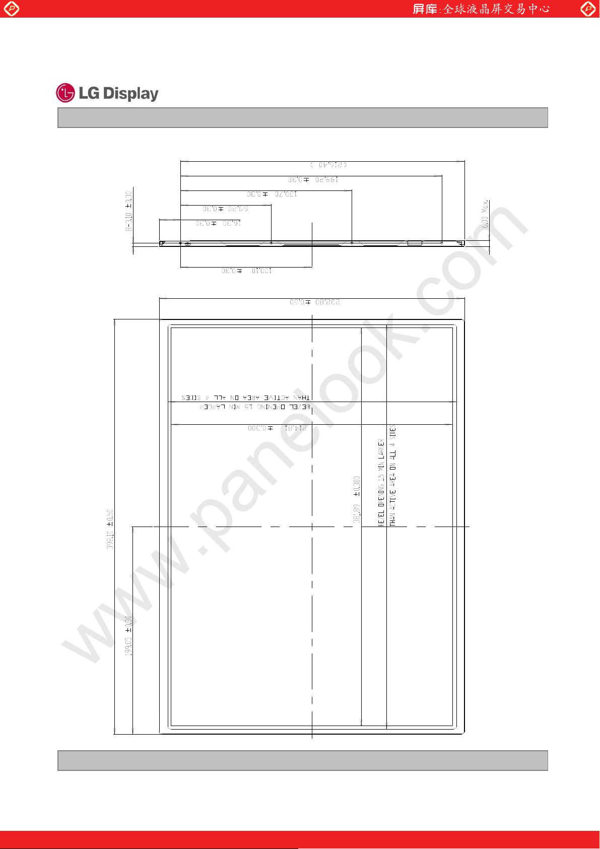
5. Mechanical Characteristics
The contents provide general mechanical characteristics for the model LP173WD1.
In addition the figures in the next page are detailed mechanical drawing of the LCD.
www.panelook.com
LP173WD1
Liquid Crystal Display
Product Specification
398.1 r 0.50mmHorizontal
Outline Dimension
Bezel Area
Active Display Area
232.8 r 0.50mmVertical
6.0mm(Max.) Depth
1.5mm Min.( Lager than Active Display Area )Horizontal
1.5mm Min.( Lager than Active Display Area )Vertical
381.89mmHorizontal
214.81 mmVertical
570g (Max.)Weight
Anti-Glare treatment of the front Polarizer (Haze 0%)Surface Treatment
Ver. 0.0 18. Sep, 2009
One step solution for LCD / PDP / OLED panel application: Datasheet, inventory and accessory!
17/ 31
www.panelook.com
Page 18
Global LCD Panel Exchange Center
www.panelook.com
LP173WD1
Liquid Crystal Display
Product Specification
<FRONT VIEW>
Note) Unit:[mm], General tolerance:
r 0.5mm
Ver. 0.0 18. Sep, 2009
One step solution for LCD / PDP / OLED panel application: Datasheet, inventory and accessory!
18/ 31
www.panelook.com
Page 19

Global LCD Panel Exchange Center
www.panelook.com
LP173WD1
Liquid Crystal Display
Product Specification
<REAR VIEW>
Note) Unit:[mm], General tolerance:
r 0.5mm
Ver. 0.0 18. Sep, 2009
One step solution for LCD / PDP / OLED panel application: Datasheet, inventory and accessory!
19/ 31
www.panelook.com
Page 20

Global LCD Panel Exchange Center
[ DETAIL DESCRIPTION OF SIDE MOUNTING SCREW ]
www.panelook.com
LP173WD1
Liquid Crystal Display
Product Specification
Ver. 0.0 18. Sep, 2009
One step solution for LCD / PDP / OLED panel application: Datasheet, inventory and accessory!
20/ 31
www.panelook.com
Page 21

Global LCD Panel Exchange Center
LGD Proposal for system cover design.(Appendix)
www.panelook.com
LP173WD1
Liquid Crystal Display
Product Specification
1
Gap check for securing the enough gap between LCM
and System cover.
Max Thickness
Sponge
LCM Reflector Side
System Cover
S-PCB
A Boundary Line
1.Rear side of LCM is sensitive against external stress,and previous check
about interference is highly needed.
Define
2.In case there is something from system cover comes into the boundary
above,mechanical interference may cause the FOS defects.
(Eg:Ripple,White spot..)
Check if antenna cable is sufficiently apart from T-CON of LCD Module.2
Define
NO GOOD
1.If system antenna is overlapped with T-CON,it might be cause the noise.
Ver. 0.0 18. Sep, 2009
GOOD
21/ 31
One step solution for LCD / PDP / OLED panel application: Datasheet, inventory and accessory!
www.panelook.com
Page 22

Global LCD Panel Exchange Center
LGD Proposal for system cover design.
www.panelook.com
LP173WD1
Liquid Crystal Display
Product Specification
3
Gap check for securing the enough gap between LCM
and System hinge.
LCM Reflector Side
Side Mount Screw Hole (4ea)
1.At least 2.0mm of gap needs to be secured to prevent the shock
Define
related defects.
S-PCB
Hinge
GAP:Min2.0mm
(“I” TYPE)
COF
(D-IC)
(“L” TYPE)
2.”L” type of hinge is recommended than “I” type under shock test.
4
Checking the path of the System wire.
Good
Ok
Bad
1.COF area needs to be handled with care.
2.GOOD ÎWire path design to system side.
Define
OKÎ Wire path is located between COFs.
BADÎWire path overlapped with COF area.
Ver. 0.0 18. Sep, 2009
#1
#1#2#3#4#5#6#7#8
22/ 31
One step solution for LCD / PDP / OLED panel application: Datasheet, inventory and accessory!
www.panelook.com
Page 23

Global LCD Panel Exchange Center
LGD Proposal for system cover design.
5 Using a bracket on the top of LCM is not recommended.
bracket
www.panelook.com
LP173WD1
Liquid Crystal Display
Product Specification
Define
With bracket Without bracket
1.Condition without bracket is good for mechanical noise,and can minimize
the light leakage from deformation of bracket.
2.The results shows that there is no difference between the condition
with or without bracket.
Securing additional gap on CNT area..6
System cover inner side.
User connector
A
A~A-1
A-1
cut
FPC:Flexible Printed Circuit.
area.
User connector
Cable pathway.
1.CNT area is specially sensitive against external stress,and additional
Define
gap by cutting on system cover will be helpful on removing the Ripple.
2.Using a thinner CNT will be better. (eg: FPC type)
Ver. 0.0 18. Sep, 2009
One step solution for LCD / PDP / OLED panel application: Datasheet, inventory and accessory!
23/ 31
www.panelook.com
Page 24

Global LCD Panel Exchange Center
6. Reliability
Environment test condition
www.panelook.com
LP173WD1
Liquid Crystal Display
Product Specification
ConditionsTest ItemNo.
Ta= 60qC, 240hHigh temperature storage test1
Ta= -20qC, 240hLow temperature storage test2
Ta= 50qC, 50%RH, 240hHigh temperature operation test3
Ta= 0qC, 240hLow temperature operation test4
Vibration test (non-operating)5
Sine wave, 5 ~ 150Hz, 1.5G, 0.37oct/min
3 axis, 30min/axis
Shock test (non-operating)6
Half sine wave, 180G, 2ms
one shock of each six faces(I.e. run 180G 2ms
for all six faces)
Altitude operating
7
storage / shipment
8
Image Sticking
1)
0 ~ 10,000 feet (3,048m) 24Hr
0 ~ 40,000 feet (12,192m) 24Hr
Ta= 25qC, Pattern : Mosaic(8 by 6),
Operating Time : 30 min
Lamp Operating Current : 6.0mA
{ Result Evaluation Criteria }
There should be no change which might affect the practical display function when the display quality
test is conducted under normal operating condition.
1)
After 30 minutes
Mosaic Pattern(8 by 6)
Half Gray
<Judgment Condition>
: Operating during 30 minutes with Mosaic Pattern(8 by 6), there is no Image Sticking
after 10 second with half gray pattern.
Ver. 0.0 18. Sep, 2009
One step solution for LCD / PDP / OLED panel application: Datasheet, inventory and accessory!
24/ 31
www.panelook.com
Page 25

Global LCD Panel Exchange Center
7. International Standards
7-1. Safety
a) UL 60950-1:2003, First Edition, Underwriters Laboratories, Inc.,
Standard for Safety of Information Technology Equipment.
b) CAN/CSA C22.2, No. 60950-1-03 1
Standard for Safety of Information Technology Equipment.
c) EN 60950-1:2001, First Edition,
European Committee for Electrotechnical Standardization(CENELEC)
European Standard for Safety of Information Technology Equipment.
www.panelook.com
Liquid Crystal Display
Product Specification
st
Ed. April 1, 2003, Canadian Standards Association,
LP173WD1
7-2. EMC
a) ANSI C63.4 “Methods of Measurement of Radio-Noise Emissions from Low-Voltage Electrical and
Electrical Equipment in the Range of 9kHZ to 40GHz. “American National Standards Institute(ANSI),
1992
b) CISPR22 “Limits and Methods of Measurement of Radio Interface Characteristics of Information
Technology Equipment.“ International Special Committee on Radio Interference.
c) EN 55022 “Limits and Methods of Measurement of Radio Interface Characteristics of Information
Technology Equipment.“ European Committee for Electrotechnical Standardization.(CENELEC), 1998
( Including A1: 2000 )
Ver. 0.0 18. Sep, 2009
One step solution for LCD / PDP / OLED panel application: Datasheet, inventory and accessory!
25/ 31
www.panelook.com
Page 26

Global LCD Panel Exchange Center
8. Packing
8-1. Designation of Lot Mark
a) Lot Mark
ABCDEFGHI JKLM
A,B,C : SIZE(INCH) D : YEAR
E : MONTH F ~ M : SERIAL NO.
www.panelook.com
LP173WD1
Liquid Crystal Display
Product Specification
Note
1. YEAR
Year
Mark
321
200452005
4
200320022001
2006720078200892009
6
2. MONTH
Month
Mark
Apr5May
4
Jun7Jul8Aug9Sep
6
b) Location of Lot Mark
Serial No. is printed on the label. The label is attached to the backside of the LCD module.
This is subject to change without prior notice.
8-2. Packing Form
a) Package quantity in one box : 20pcs
2010
0
Oct
A
Nov
B
DecMarFebJan
C321
b) Box Size :490X390X298
Ver. 0.0 18. Sep, 2009
One step solution for LCD / PDP / OLED panel application: Datasheet, inventory and accessory!
26/ 31
www.panelook.com
Page 27
Global LCD Panel Exchange Center
9. PRECAUTIONS
Please pay attention to the followings when you use this TFT LCD module.
9-1. MOUNTING PRECAUTIONS
(1) You must mount a module using holes arranged in four corners or four sides.
(2) You should consider the mounting structure so that uneven force (ex. Twisted stress) is not applied to the
module. And the case on which a module is mounted should have sufficient strength so that external
force is not transmitted directly to the module.
(3) Please attach the surface transparent protective plate to the surface in order to protect the polarizer.
Transparent protective plate should have sufficient strength in order to the resist external force.
(4) You should adopt radiation structure to satisfy the temperature specification.
(5) Acetic acid type and chlorine type materials for the cover case are not desirable because the former
generates corrosive gas of attacking the polarizer at high temperature and the latter causes circuit break
by electro-chemical reaction.
(6) Do not touch, push or rub the exposed polarizers with glass, tweezers or anything harder than HB
pencil lead. And please do not rub with dust clothes with chemical treatment.
Do not touch the surface of polarizer for bare hand or greasy cloth.(Some cosmetics are detrimental
to the polarizer.)
(7) When the surface becomes dusty, please wipe gently with absorbent cotton or other soft materials like
chamois soaks with petroleum benzene. Normal-hexane is recommended for cleaning the adhesives
used to attach front / rear polarizers. Do not use acetone, toluene and alcohol because they cause
chemical damage to the polarizer.
(8) Wipe off saliva or water drops as soon as possible. Their long time contact with polarizer causes
deformations and color fading.
(9) Do not open the case because inside circuits do not have sufficient strength.
www.panelook.com
LP173WD1
Liquid Crystal Display
Product Specification
9-2. OPERATING PRECAUTIONS
(1) The spike noise causes the mis-operation of circuits. It should be lower than following voltage :
V=· 200mV(Over and under shoot voltage)
(2) Response time depends on the temperature.(In lower temperature, it becomes longer.)
(3) Brightness depends on the temperature. (In lower temperature, it becomes lower.)
And in lower temperature, response time(required time that brightness is stable after turned on) becomes
longer.
(4) Be careful for condensation at sudden temperature change. Condensation makes damage to polarizer or
electrical contacted parts. And after fading condensation, smear or spot will occur.
(5) When fixed patterns are displayed for a long time, remnant image is likely to occur.
(6) Module has high frequency circuits. Sufficient suppression to the electromagnetic interference shall be
done by system manufacturers. Grounding and shielding methods may be important to minimized the
interference.
Ver. 0.0 18. Sep, 2009
27/ 31
One step solution for LCD / PDP / OLED panel application: Datasheet, inventory and accessory!
www.panelook.com
Page 28

Global LCD Panel Exchange Center
9-3. ELECTROSTATIC DISCHARGE CONTROL
Since a module is composed of electronic circuits, it is not strong to electrostatic discharge. Make certain that
treatment persons are connected to ground through wrist band etc. And don’t touch interface pin directly.
9-4. PRECAUTIONS FOR STRONG LIGHT EXPOSURE
Strong light exposure causes degradation of polarizer and color filter.
9-5. STORAGE
www.panelook.com
LP173WD1
Liquid Crystal Display
Product Specification
When storing modules as spares for a long time, the following precautions are necessary.
(1) Store them in a dark place. Do not expose the module to sunlight or fluorescent light. Keep the
temperature between 5qC and 35qC at normal humidity.
(2) The polarizer surface should not come in contact with any other object.
It is recommended that they be stored in the container in which they were shipped.
9-6. HANDLING PRECAUTIONS FOR PROTECTION FILM
(1) When the protection film is peeled off, static electricity is generated between the film and polarizer.
This should be peeled off slowly and carefully by people who are electrically grounded and with well
ion-blown equipment or in such a condition, etc.
(2) The protection film is attached to the polarizer with a small amount of glue. If some stress is applied
to rub the protection film against the polarizer during the time you peel off the film, the glue is apt to
remain on the polarizer.
Please carefully peel off the protection film without rubbing it against the polarizer.
(3) When the module with protection film attached is stored for a long time, sometimes there remains a
very small amount of glue still on the polarizer after the protection film is peeled off.
(4) You can remove the glue easily. When the glue remains on the polarizer surface or its vestige is
recognized, please wipe them off with absorbent cotton waste or other soft material like chamois
soaked with normal-hexane.
Ver. 0.0 18. Sep, 2009
One step solution for LCD / PDP / OLED panel application: Datasheet, inventory and accessory!
28/ 31
www.panelook.com
Page 29

Global LCD Panel Exchange Center
ٻٻڧ ګ ڌ ڒ ڎ ڲ ڟ ڌ ڈ گ ڧ ڟ ڎ ٻڠ ڈ ڠ ڟ ڤڟ ٻڟ ڜ گ ڜ ٻڃۑۀ ۍڋ ډڋ ڄ
ڄ
ڣ ۀ ڼ ڿ ۀ ۍ
ڱ ۀ ۉ ڿ ۀ ۍڊ
ګ ۍۊ ڿ ې ھ ۏٻڤڟ
ڠ ڟ ڤڟ ٻڱ ۀ ۍێۄۊ ۉ ڊ
ڭ ۀ ۑ ۄێ ۄۊ ۉ
ڟ ۄێ ۋ ۇڼ ۔ ٻ
ګ ڼ ۍڼ ۈ ۀ ۏۀ ۍ
ڞ ۊ ۇۊ ۍ
ڞ ۃ ڼ ۍڼ ھ ۏۀ ۍۄێ ۏۄھ
ڠ ێ ۏڼ ڽ ۇۄێ ۃ ۀ ڿ
گ ۄۈ ۄۉ ۂ ێ
ڮ ۏڼ ۉ ڿ ڼ ۍڿ
گ ۄۈ ۄۉ ۂ ٻڤڟ
APPENDIX A. Enhanced Extended Display Identification Data (EEDIDTM) 1/3
www.panelook.com
LP173WD1
Liquid Crystal Display
Product Specification
ڝ۔ۏۀپ ڝ۔ۏۀپ
ڃڿۀھۄۈ ڼۇ
ڃڣ ڠ ڳ ڄ
ڋڋڋڣۀڼڿۀۍ ڋڋ
ڌڋڌ ڡڡ
ڍڋڍ ڡڡ
ڎڋڎ ڡڡ
ڏڋڏ ڡڡ
ڐڋڐ ڡڡ
ڑڋڑ ڡڡ
ڒڋڒ ڋڋ
ړ ڋړ ڠ ڤڮ ڜ ٻۈ ڼۉېہڼھۏېۍۀۍٻھۊ ڿۀٻژٻڧڢ ڟ ڎ ڋ
ڔڋڔ ڠڏ
ڌڋ ڋڜ ګۍۊڿېھۏٻھۊڿۀٻژٻڋڍڒڝ ڒ ڝ
ڌ ڌ ڋ ڝ ڃڣ ۀ ۓ ڇٻڧ ڮ ڝ ٻہۄۍێ ۏڄ ڋ ڍ
ڌ ڍ ڋ ڞ ڎ ڍ ڈ ڽ ۄۏٻ ێ ۀ ۍۄڼ ۇٻ ۉ ې ۈ ڽ ۀ ۍٻ ڋ ڋ
ڌڎ ڋڟ ڋڋ
ڌڏ ڋڠ ڋڋ
ڌڐ ڋڡ ڋڋ
ڌڑ ڌڋ ڲ ۀۀۆٻۊہٻۈ ڼۉېہڼھۏېۍۀ ڋ ڋ
ڌڒ ڌڌ ڴۀڼۍٻۊہٻۈ ڼۉېہڼھۏېۍۀٻژٻڍڋڋڔ ڌ ڎ
ڌړ ڌڍ ڠڟ ڤڟ ٻڮۏۍېھۏېۍۀٻۑۀۍێۄۊ ۉٻپٻژٻڌ ڋ ڌ
ڌڔ ڌڎ ڠڟ ڤڟ ٻڭۀۑۄێۄۊۉٻپٻژٻڎ ڋ ڎ
ڍڋ ڌڏ ڱۄڿۀۊٻۄۉۋېۏٻڿۀہۄۉۄۏۄۊۉٻژٻڟ ۄۂۄۏڼۇٻڤڊۋڇۉۊۉٻگڨ ڟ ڮ ٻڞ ڭڢ ڝ ړ ڋ
ڍڌ ڌڐ ڨ ڼۓٻڣ ٻۄۈ ڼۂۀٻێۄەۀڃ༃ڄٻژٻڎړډڍڋړ༃ڃڎړڄ ڍ ڑ
ڍڍ ڌڑ ڨ ڼۓٻڱٻۄۈ ڼۂۀٻێۄەۀڃ༃ڄٻژٻڍڌډڏڔڍ༃ڃڍڌڄ ڌ ڐ
ڍڎ ڌڒ ڟ ۄێۋۇڼ۔ٻۂڼۈ ۈ ڼٻژٻڍډڍڋ ڒ ړ
ڍڏ ڌړ ڡۀڼۏېۍۀٻێېۋۋۊۍۏڃڟ ګڨ ڮڄٻژٻڜھۏۄۑۀٻۊہہڇٻڭڢ ڝ ٻڞۊۇۊۍ ڋ ڜ
ڍڐ ڌڔ ڭۀڿڊڢ ۍۀۀۉٻۇۊے ٻڝ ۄۏێ
ڍ ڑ ڌ ڜ ڝ ۇې ۀ ڊ ڲ ۃ ۄۏۀ ٻڧ ۊ ے ٻڝ ۄۏێ
ڍ ڒ ڌ ڝ ڭ ۀ ڿ ٻڳ ٻٻٻٻٻٻٻٻٻٻٻٻٻٻٻٻٻٻٻٻٻٻڭ ۓ ٻژ ٻڋ ډڑ ڌ ڑ
ڍ ړ ڌ ڞ ڭ ۀ ڿ ٻڴ ٻٻٻٻٻٻٻٻٻٻٻٻٻٻٻٻٻٻٻٻٻٻڭ ۔ ٻژ ٻڋ ډڎ ڏ ڑ
ڍ ڔ ڌ ڟ ڢ ۍۀ ۀ ۉ ٻڳ ٻٻٻٻٻٻٻٻٻٻٻٻٻٻٻٻٻٻٻڢ ۓ ٻژ ٻڋ ډڎ ڌ ڐ
ڎ ڋ ڌ ڠ ڢ ۍۀ ۀ ۉ ٻڴ ٻٻٻٻٻٻٻٻٻٻٻٻٻٻٻٻٻٻٻڢ ۔ ٻژ ٻڋ ډڑ ڋ ڍ
ڎ ڌ ڌ ڡ ڝ ۇې ۀ ٻڳ ٻٻٻٻٻٻٻٻٻٻٻٻٻٻٻٻٻٻٻٻٻڝ ۓ ٻژ ٻڋ ډڌ ڐ ڍ
ڎ ڍ ڍ ڋ ڝ ۇې ۀ ٻڴ ٻٻٻٻٻٻٻٻٻٻٻٻٻٻٻٻٻٻٻٻٻڝ ۔ ٻژ ٻڋ ډڌ ڌ ڋ
ڎ ڎ ڍ ڌ ڲ ۃ ۄۏۀ ٻڳ ٻٻٻٻٻٻٻٻٻٻٻٻٻٻٻٻٻٻٻٻڲ ۓ ٻژ ٻڋ ډڎ ڌ ڎ
ڎ ڏ ڍ ڍ ڲ ۃ ۄۏۀ ٻڴ ٻٻٻٻٻٻٻٻٻٻٻٻٻٻٻٻٻٻٻٻڲ ۔ ٻژ ٻڋ ډڎ ڍ ڔ
ڎڐ ڍڎ ڠێۏڼڽۇۄێۃۀڿٻگۄۈ ۄۉۂٻڤ ڋ ڋ
ڎڑ ڍڏ ڠێۏڼڽۇۄێۃۀڿٻگۄۈ ۄۉۂٻڤڤ ڋ ڋ
ڎڒ ڍڐ ڨ ڼۉېہڼھۏېۍۀۍڂێٻگۄۈ ۄۉۂێ ڋ ڋ
ڎ ړ ڍ ڑ ڮ ۏڼ ۉ ڿ ڼ ۍڿ ٻگ ۄۈ ۄۉ ۂ ٻڤڿ ۀ ۉ ۏۄہۄھ ڼ ۏۄۊ ۉ ٻڌ ٻے ڼ ێ ٻۉ ۊ ۏٻې ێ ۀ ڿ
ڎ ڔ ڍ ڒ ڮ ۏڼ ۉ ڿ ڼ ۍڿ ٻگ ۄۈ ۄۉ ۂ ٻڤڿ ۀ ۉ ۏۄہۄھ ڼ ۏۄۊ ۉ ٻڌ ٻے ڼ ێ ٻۉ ۊ ۏٻې ێ ۀ ڿ
ڏ ڋ ڍ ړ ڮ ۏڼ ۉ ڿ ڼ ۍڿ ٻگ ۄۈ ۄۉ ۂ ٻڤڿ ۀ ۉ ۏۄہۄھ ڼ ۏۄۊ ۉ ٻڍ ٻے ڼ ێ ٻۉ ۊ ۏٻې ێ ۀ ڿ
ڏ ڌ ڍ ڔ ڮ ۏڼ ۉ ڿ ڼ ۍڿ ٻگ ۄۈ ۄۉ ۂ ٻڤڿ ۀ ۉ ۏۄہۄھ ڼ ۏۄۊ ۉ ٻڍ ٻے ڼ ێ ٻۉ ۊ ۏٻې ێ ۀ ڿ
ڏ ڍ ڍ ڜ ڮ ۏڼ ۉ ڿ ڼ ۍڿ ٻگ ۄۈ ۄۉ ۂ ٻڤڿ ۀ ۉ ۏۄہۄھ ڼ ۏۄۊ ۉ ٻڎ ٻے ڼ ێ ٻۉ ۊ ۏٻې ێ ۀ ڿ
ڏ ڎ ڍ ڝ ڮ ۏڼ ۉ ڿ ڼ ۍڿ ٻگ ۄۈ ۄۉ ۂ ٻڤڿ ۀ ۉ ۏۄہۄھ ڼ ۏۄۊ ۉ ٻڎ ٻے ڼ ێ ٻۉ ۊ ۏٻې ێ ۀ ڿ
ڏ ڏ ڍ ڞ ڮ ۏڼ ۉ ڿ ڼ ۍڿ ٻگ ۄۈ ۄۉ ۂ ٻڤڿ ۀ ۉ ۏۄہۄھ ڼ ۏۄۊ ۉ ٻڏ ٻے ڼ ێ ٻۉ ۊ ۏٻې ێ ۀ ڿ
ڏ ڐ ڍ ڟ ڮ ۏڼ ۉ ڿ ڼ ۍڿ ٻگ ۄۈ ۄۉ ۂ ٻڤڿ ۀ ۉ ۏۄہۄھ ڼ ۏۄۊ ۉ ٻڏ ٻے ڼ ێ ٻۉ ۊ ۏٻې ێ ۀ ڿ
ڏ ڑ ڍ ڠ ڮ ۏڼ ۉ ڿ ڼ ۍڿ ٻگ ۄۈ ۄۉ ۂ ٻڤڿ ۀ ۉ ۏۄہۄھ ڼ ۏۄۊ ۉ ٻڐ ٻے ڼ ێ ٻۉ ۊ ۏٻې ێ ۀ ڿ
ڏ ڒ ڍ ڡ ڮ ۏڼ ۉ ڿ ڼ ۍڿ ٻگ ۄۈ ۄۉ ۂ ٻڤڿ ۀ ۉ ۏۄہۄھ ڼ ۏۄۊ ۉ ٻڐ ٻے ڼ ێ ٻۉ ۊ ۏٻې ێ ۀ ڿ
ڏ ړ ڎ ڋ ڮ ۏڼ ۉ ڿ ڼ ۍڿ ٻگ ۄۈ ۄۉ ۂ ٻڤڿ ۀ ۉ ۏۄہۄھ ڼ ۏۄۊ ۉ ٻڑ ٻے ڼ ێ ٻۉ ۊ ۏٻې ێ ۀ ڿ
ڏ ڔ ڎ ڌ ڮ ۏڼ ۉ ڿ ڼ ۍڿ ٻگ ۄۈ ۄۉ ۂ ٻڤڿ ۀ ۉ ۏۄہۄھ ڼ ۏۄۊ ۉ ٻڑ ٻے ڼ ێ ٻۉ ۊ ۏٻې ێ ۀ ڿ
ڐ ڋ ڎ ڍ ڮ ۏڼ ۉ ڿ ڼ ۍڿ ٻگ ۄۈ ۄۉ ۂ ٻڤڿ ۀ ۉ ۏۄہۄھ ڼ ۏۄۊ ۉ ٻڒ ٻے ڼ ێ ٻۉ ۊ ۏٻې ێ ۀ ڿ
ڐ ڌ ڎ ڎ ڮ ۏڼ ۉ ڿ ڼ ۍڿ ٻگ ۄۈ ۄۉ ۂ ٻڤڿ ۀ ۉ ۏۄہۄھ ڼ ۏۄۊ ۉ ٻڒ ٻے ڼ ێ ٻۉ ۊ ۏٻې ێ ۀ ڿ
ڐ ڍ ڎ ڏ ڮ ۏڼ ۉ ڿ ڼ ۍڿ ٻگ ۄۈ ۄۉ ۂ ٻڤڿ ۀ ۉ ۏۄہۄھ ڼ ۏۄۊ ۉ ٻړ ٻے ڼ ێ ٻۉ ۊ ۏٻې ێ ۀ ڿ
ڐ ڎ ڎ ڐ ڮ ۏڼ ۉ ڿ ڼ ۍڿ ٻگ ۄۈ ۄۉ ۂ ٻڤڿ ۀ ۉ ۏۄہۄھ ڼ ۏۄۊ ۉ ٻړ ٻے ڼ ێ ٻۉ ۊ ۏٻې ێ ۀ ڿ
ڡ ۄۀ ۇڿ ٻک ڼ ۈ ۀ ٻڼ ۉ ڿ ٻڞ ۊ ۈ ۈ ۀ ۉ ۏێ
ڱڼۇېۀ
ڃڣ ڠ ڳ ڄ
A8
C0
9D
58
50
9A
26
1C
50
54
ڋ ڌ ڋڋڋڋ ڋڋڋڌ
ڋ ڌ ڋڋڋڋ ڋڋڋڌ
ڋ ڌ ڋڋڋڋ ڋڋڋڌ
ڋ ڌ ڋڋڋڋ ڋڋڋڌ
ڋ ڌ ڋڋڋڋ ڋڋڋڌ
ڋ ڌ ڋڋڋڋ ڋڋڋڌ
ڋ ڌ ڋڋڋڋ ڋڋڋڌ
ڋ ڌ ڋڋڋڋ ڋڋڋڌ
ڋ ڌ ڋڋڋڋ ڋڋڋڌ
ڋ ڌ ڋڋڋڋ ڋڋڋڌ
ڋ ڌ ڋڋڋڋ ڋڋڋڌ
ڋ ڌ ڋڋڋڋ ڋڋڋڌ
ڋ ڌ ڋڋڋڋ ڋڋڋڌ
ڋ ڌ ڋڋڋڋ ڋڋڋڌ
ڋ ڌ ڋڋڋڋ ڋڋڋڌ
ڋ ڌ ڋڋڋڋ ڋڋڋڌ
ڱڼۇېۀ
ڃڽ ۄۉ ڼ ۍ۔ ڄ
ڋڋڋڋ ڋڋڋڋ
ڌڌڌڌ ڌڌڌڌ
ڌڌڌڌ ڌڌڌڌ
ڌڌڌڌ ڌڌڌڌ
ڌڌڌڌ ڌڌڌڌ
ڌڌڌڌ ڌڌڌڌ
ڌڌڌڌ ڌڌڌڌ
ڋڋڋڋ ڋڋڋڋ
ڋڋڌڌ ڋڋڋڋ
ڌڌڌڋ ڋڌڋڋ
ڋڌڌڌ ڌڋڌڌ
ڋڋڋڋ ڋڋڌڋ
ڋڋڋڋ ڋڋڋڋ
ڋڋڋڋ ڋڋڋڋ
ڋڋڋڋ ڋڋڋڋ
ڋڋڋڋ ڋڋڋڋ
ڋڋڋڋ ڋڋڋڋ
ڋڋڋڌ ڋڋڌڌ
ڋڋڋڋ ڋڋڋڌ
ڋڋڋڋ ڋڋڌڌ
ڌڋڋڋ ڋڋڋڋ
ڋڋڌڋ ڋڌڌڋ
ڋڋڋڌ ڋڌڋڌ
ڋڌڌڌ ڌڋڋڋ
ڋڋڋڋ ڌڋڌڋ
ڌڋڌڋ ڌڋڋڋ
ڌڌڋڋ ڋڋڋڋ
ڌڋڋڌ ڌڌڋڌ
ڋڌڋڌ ڌڋڋڋ
ڋڌڋڌ ڋڋڋڋ
ڌڋڋڌ ڌڋڌڋ
ڋڋڌڋ ڋڌڌڋ
ڋڋڋڌ ڌڌڋڋ
ڋڌڋڌ ڋڋڋڋ
ڋڌڋڌ ڋڌڋڋ
ڋڋڋڋ ڋڋڋڋ
ڋڋڋڋ ڋڋڋڋ
ڋڋڋڋ ڋڋڋڋ
ڍڋڋڔڈڋڔډڌړ
Ver. 0.0 18. Sep, 2009
One step solution for LCD / PDP / OLED panel application: Datasheet, inventory and accessory!
29/ 31
www.panelook.com
Page 30

Global LCD Panel Exchange Center
ڄ
گ ۄۈ ۄۉ ۂ
ڟ ۀ ێ ھ ۍۄۋ ۏۊۍ
پ ڌ
ڟ ۀ ۏڼۄۇۀڿ
گ ۄۈ ۄۉ ۂ
ڟ ۀ ێ ھ ۍۄۋ ۏۄۊ ۉ
پ ڍ
ڟ ۀ ۏڼۄۇۀڿ
گ ۄۈ ۄۉ ۂ
ڟ ۀ ێ ھ ۍۄۋ ۏۄۊ ۉ
پ ڎ
APPENDIX A. Enhanced Extended Display Identification Data (EEDIDTM) 2/3
www.panelook.com
LP173WD1
Liquid Crystal Display
Product Specification
ڝ۔ۏۀپ ڝ۔ۏۀپ
ڃڿ ۀ ھ ۄۈ ڼ ۇ
ڐڏ ڎڑ ڌڑڋڋٻڳٻڔڋڋٻڛ ٻڑڋ༨ٻۈ ۊڿۀٻڕٻۋۄۓۀۇٻھۇۊھۆٻژٻڔڒډڒڐڨ ڣ ە
ڐ ڐ ڎ ڒ ڃڮ ۏۊ ۍۀ ڿ ٻڧ ڮ ڝ ٻہۄۍێ ۏڄ
ڐڑ ڎړ ڣۊۍۄەۊۉۏڼۇٻڜ ھۏۄۑۀٻژٻڌڑڋڋٻۋۄۓۀۇێ
ڐڒ ڎڔ ڣ ۊۍۄەۊۉۏڼۇٻڝۇڼۉۆۄۉۂٻژٻڌړڏٻۋۄۓۀۇێ
ڐړ ڎڜ ڣۊۍۄەۊۉۏڼۇٻڜ ھۏۄۑۀٻڕٻڣ ۊۍۄەۊۉۏڼۇٻڝۇڼۉۆۄۉۂٻژٻڌڑڋڋٻڕٻڌړڏ
ڐڔ ڎڝ ڱۀۍۏۄھڼۇٻڜۑۏۄۑۀٻژٻڔڋڋٻۇۄۉۀێ
ڑڋ ڎڞ ڱۀۍۏۄھڼۇٻڝۇڼۉۆۄۉۂٻژٻٻڌڍٻۇۄۉۀێ
ڑڌ ڎڟ ڱۀۍۏۄھڼۇٻڜھۏۄۑۀٻڕٻڱۀۍۏۄھڼۇٻڝۇڼۉۆۄۉۂٻژٻٻڔڋڋٻڕٻڌڍ
ڑڍ ڎڠ ڣۊۍۄەۊۉۏڼۇٻڮ ۔ۉھډٻڪ ہہێۀۏٻژٻڏړٻۋۄۓۀۇێ
ڑڎ ڎڡ ڣۊۍۄەۊۉۏڼۇٻڮ ۔ۉھٻګېۇێۀٻڲ ۄڿۏۃٻژٻڏړٻۋۄۓۀۇێ
ڑ ڏ ڏ ڋ ڱ ۀ ۍۏۄھ ڼ ۇٻڮ ۔ ۉ ھ ٻڪ ہہێ ۀ ۏٻژ ٻڍ ٻۇۄۉ ۀ ێ ڇٻڮ ۔ ۉ ھ ٻڲ ۄڿ ۏۃ ٻژ ٻڎ ٻۇۄۉ ۀ ێ
ڑڐ ڏڌ ڣۊۍۄەۊۉۏڼۇٻڱۀۍۏۄھڼۇٻٻڮ۔ۉھٻڪ ہہێۀۏڊڲ ۄڿۏۃٻېۋۋۀۍٻڍڽۄۏێٻژٻڋ ڋ ڋ ڋڋڋڋ ڋڋڋڋ
ڑڑ ڏڍ ڣۊۍۄەۊۉۏڼۇٻڤۈ ڼۂۀٻڮ ۄەۀٻژٻڎړڍډڋړ༂ڃڎړڍڄ ڒ ڠ ڋڌڌڌ ڌڌڌڋ
ڑڒ ڏڎ ڱۀۍۏۄھڼۇٻڤۈ ڼۂۀٻڮۄەۀٻژٻڍڌڏډڔڍ༂ڃڍڌڐڄ ڟ ڒ ڌڌڋڌ ڋڌڌڌ
ڑړ ڏڏ ڣۊۍۄەۊۉۏڼۇٻځ ٻڱۀۍۏۄھڼۇٻڤۈ ڼۂۀٻڮۄەۀ ڌ ڋ ڋڋڋڌ ڋڋڋڋ
ڑڔ ڏڐ ڣۊۍۄەۊۉۏڼۇٻڝ ۊۍڿۀۍٻژٻڋ ڋ ڋ ڋڋڋڋ ڋڋڋڋ
ڒڋ ڏڑ ڱۀۍۏۄھڼۇٻڝۊۍڿۀۍٻژٻڋ ڋ ڋ ڋڋڋڋ ڋڋڋڋ
ڒڌ ڏڒ
ڒڍ ڏړ ڟۀۏڼۄۇۀڿٻگۄۈ ۄۉۂٻڟ ۀێھۍۄۋۏۊۍٻپڍ ڋ ڋ ڋڋڋڋ ڋڋڋڋ
ڒڎ ڏڔ ڋ ڋ ڋڋڋڋ ڋڋڋڋ
ڒڏ ڏڜ ڋ ڋ ڋڋڋڋ ڋڋڋڋ
ڒڐ ڏڝ ڋ ڋ ڋڋڋڋ ڋڋڋڋ
ڒڑ ڏڞ ڋ ڋ ڋڋڋڋ ڋڋڋڋ
ڒڒ ڏڟ ڋ ڋ ڋڋڋڋ ڋڋڋڋ
ڒړ ڏڠ ڋ ڋ ڋڋڋڋ ڋڋڋڋ ڟ
ڒڔ ڏڡ ڋ ڋ ڋڋڋڋ ڋڋڋڋ گ
ړڋ ڐڋ ڋ ڋ ڋڋڋڋ ڋڋڋڋ ڟ
ړڌ ڐڌ ڋ ڋ ڋڋڋڋ ڋڋڋڋ پ
ړڍ ڐڍ ڋ ڋ ڋڋڋڋ ڋڋڋڋ
ړڎ ڐڎ ڋ ڋ ڋڋڋڋ ڋڋڋڋ
ړڏ ڐڐ ڋ ڋ ڋڋڋڋ ڋڋڋڋ
ړڐ ڐڐ ڋ ڋ ڋڋڋڋ ڋڋڋڋ
ړڑ ڐڑ ڋ ڋ ڋڋڋڋ ڋڋڋڋ
ړڒ ڐڒ ڋ ڋ ڋڋڋڋ ڋڋڋڋ
ړړ ڐړ ڋ ڋ ڋڋڋڋ ڋڋڋڋ
ړڔ ڐڔ ڋ ڋ ڋڋڋڋ ڋڋڋڋ
ڔڋ ڐڜ ڟۀۏڼۄۇۀڿٻگۄۈ ۄۉۂٻڟ ۀێھۍۄۋۏۊۍٻپڎ ڋ ڋ ڋڋڋڋ ڋڋڋڋ
ڔڌ ڐڝ ڋ ڋ ڋڋڋڋ ڋڋڋڋ
ڔڍ ڐڞ ڋ ڋ ڋڋڋڋ ڋڋڋڋ
ڔڎ ڐڟ ڡ ڠ ڌڌڌڌ ڌڌڌڋ
ڔڏ ڐڠ ڋ ڋ ڋڋڋڋ ڋڋڋڋ
ڔڐ ڐڡ ڋ ڋ ڋڋڋڋ ڋڋڋڋ
ڔڑ ڑڋ ڋ ڋ ڋڋڋڋ ڋڋڋڋ ڟ
ڔڒ ڑڌ ڋ ڋ ڋڋڋڋ ڋڋڋڋ گ
ڔړ ڑڍ ڧ ڏ ڞ ڋڌڋڋ ڌڌڋڋ ڟ
ڔڔ ڑڎ ڢ ڏ ڒ ڋڌڋڋ ڋڌڌڌ پ
ڌڋڋ ڑڏ ڟ ڏ ڏ ڋڌڋڋ ڋڌڋڋ
ڌڋڌ ڑڐ ۄ ڑ ڔ ڋڌڌڋ ڌڋڋڌ
ڌڋڍ ڑڑ ێ ڒ ڎ ڋڌڌڌ ڋڋڌڌ
ڌڋڎ ڑڒ ۋ ڒ ڋ ڋڌڌڌ ڋڋڋڋ
ڌڋڏ ڑړ ۇ ڑ ڞ ڋڌڌڋ ڌڌڋڋ
ڌڋڐ ڑڔ ڼ ڑ ڌ ڋڌڌڋ ڋڋڋڌ
ڌڋڑ ڑڜ ۔ ڒ ڔ ڋڌڌڌ ڌڋڋڌ
ڌڋڒ ڑڝ ڧڡ ڋ ڜ ڋڋڋڋ ڌڋڌڋ
ڃڣ ڠ ڳ ڄ
کۊۉڈۄۉۏۀۍۇڼ ھۀڿڇک ۊۍۈ ڼ ۇٻڿۄێ ۋ ۇڼ ۔ ڇۉ ۊ ٻێ ۏۀ ۍۀ ۊ ڇڟ ۄۂ ۄۏڼ ۇٻێ ۀ ۋ ڼ ۍڼ ۏۀ ٻێ ۔ ۉ ھ ڇ ڣ ڊ ڱ ٻۋ ۊ ۇٻۉ ۀ ۂ ڼ ۏۄۑ ۀ ێ
ڡۄۀۇڿٻک ڼۈ ۀٻڼۉڿٻڞ ۊۈ ۈ ۀۉۏێ
ڱڼۇېۀ
ڃڣ ڠ ڳ ڄ
2F
26
40
B8
60
84
0C
30
30
30
23
ڌ ڔ ڋڋڋڌ ڌڋڋڌ
ڱڼۇېۀ
ڃڽ ۄۉ ڼ ۍ۔ ڄ
ڋڋڌڋ ڌڌڌڌ
ڋڋڌڋ ڋڌڌڋ
ڋڌڋڋ ڋڋڋڋ
ڌڋڌڌ ڌڋڋڋ
ڋڌڌڋ ڋڋڋڋ
ڌڋڋڋ ڋڌڋڋ
ڋڋڋڋ ڌڌڋڋ
ڋڋڌڌ ڋڋڋڋ گ
ڋڋڌڌ ڋڋڋڋ ڟ
ڋڋڌڌ ڋڋڋڋ پ
ڋڋڌڋ ڋڋڌڌ
Ver. 0.0 18. Sep, 2009
One step solution for LCD / PDP / OLED panel application: Datasheet, inventory and accessory!
30/ 31
www.panelook.com
Page 31

Global LCD Panel Exchange Center
ڄ
ڟ ۀۏڼۄۇۀڿ
گۄۈ ۄۉۂ
ڟ ۀێھۍۄۋۏۄۊۉ
پڏ
ڠۓۏۀۉێۄۊۉٻڡۇڼۂ
ڞ ۃۀھۆێېۈ
APPENDIX A. Enhanced Extended Display Identification Data (EEDIDTM) 3/3
www.panelook.com
LP173WD1
Liquid Crystal Display
Product Specification
ڝ۔ۏۀپ ڝ۔ۏۀپ
ڃڿ ۀ ھ ۄۈڼۇ
ڌڋړ ڑڞ ڟ ۀۏڼۄۇۀڿٻگۄۈۄۉۂٻڟ ۀێھۍۄۋۏۊۍٻپڏ ڋ ڋ ڋڋڋڋ ڋڋڋڋ
ڌڋڔ ڑڟ ڋ ڋ ڋڋڋڋ ڋڋڋڋ
ڌڌڋ ڑڠ ڋ ڋ ڋڋڋڋ ڋڋڋڋ
ڌڌڌ ڑڡ ڡ ڠ ڌڌڌڌ ڌڌڌڋ
ڌڌڍ ڒڋ ڋ ڋ ڋڋڋڋ ڋڋڋڋ
ڌڌڎ ڒڌ ڧ ڏ ڞ ڋڌڋڋ ڌڌڋڋ
ڌڌڏ ڒڍ ګ ڐ ڋ ڋڌڋڌ ڋڋڋڋ ڟ
ڌڌڐ ڒڎ ڌ ڎ ڌ ڋڋڌڌ ڋڋڋڌ گ
ڌڌڑ ڒڏ ڒ ڎ ڒ ڋڋڌڌ ڋڌڌڌ ڟ
ڌڌڒ ڒڐ ڎ ڎ ڎ ڋڋڌڌ ڋڋڌڌ پ
ڌڌړ ڒڑ ڲ ڐ ڒ ڋڌڋڌ ڋڌڌڌ
ڌڌڔ ڒڒ ڟ ڏ ڏ ڋڌڋڋ ڋڌڋڋ
ڌڍڋ ڒړ ڌ ڎ ڌ ڋڋڌڌ ڋڋڋڌ
ڌڍڌ ڒڔ ڈ ڍ ڟ ڋڋڌڋ ڌڌڋڌ
ڌڍڍ ڒڜ گ ڐ ڏ ڋڌڋڌ ڋڌڋڋ
ڌڍڎ ڒڝ ڧ ڏ ڞ ڋڌڋڋ ڌڌڋڋ
ڌڍڏ ڒڞ ڟ ڏ ڏ ڋڌڋڋ ڋڌڋڋ
ڌڍڐ ڒڟ ڎ ڎ ڎ ڋڋڌڌ ڋڋڌڌ
ڌڍڑ ڒڠ ڠۓۏۀۉێۄۊۉٻہۇڼ ۂ ٻژ ٻڋ ڋ ڋ ڋ ڋ ڋ ڋ ڋ ڋ ڋ ڋ ڋ ڠ
ڌڍڒ ڒڡ ڞ ۃۀھۆێېۈ ڞ ڋ ڌڌڋڋ ڋڋڋڋ ڞ
ڃڣ ڠ ڳ ڄ
ڡۄۀۇڿٻکڼۈۀٻڼۉڿٻڞۊۈۈۀۉۏێ
ڱڼۇېۀ
ڃڣ ڠ ڳ ڄ
ڱڼۇېۀ
ڃڽ ۄۉڼۍ۔ڄ
Ver. 0.0 18. Sep, 2009
One step solution for LCD / PDP / OLED panel application: Datasheet, inventory and accessory!
31/ 31
www.panelook.com
 Loading...