

Page 1
SPECIFICATION
(◆) Preliminary Specification
( ) Final Specification
Title 19.0” SXGA TFT LCD
LM190E0A
Liquid Crystal Display
Product Specification
FOR
APPROVAL
BUYER
MODEL
SIGNATURE DATE
/
/
/
General
SUPPLIER LG Display Co., Ltd.
*MODEL LM190E0A
SUFFIX SLA1
*When you obtain standard approval,
please use the above model name without suffix
APPROVED BY
C. K. Lee / G.Manager
REVIEWED BY
H. S. Kim / Manager [C]
C.H. Song / Manager [M]
J. S. Pyo / Manager [P]
PREPARED BY
C. Y. Sung / Engineer
DATE
Please return 1 copy for your confirmation
With your signature and comments.
Ver. 0.3 Mar. 28, 2013
Product Engineering Dept.
LG Display Co., Ltd
1 / 30
Page 2
Product Specification
Contents
LM190E0A
Liquid Crystal Display
No ITEM
COVER 1
CONTENTS 2
RECORD OF REVISIONS 3
1 GENERAL DESCRIPTION 4
2 ABSOLUTE MAXIMUM RATINGS 5
3 ELECTRICAL SPECIFICATIONS 6
1) ELECTRICAL CHARACTERISTICS 6
2) INTERFACE CONNECTIONS 8
3) LVDS characteristics 11
4) SIGNAL TIMING SPECIFICATIONS 14
5) SIGNAL TIMING WAVEFORMS 15
6) COLOR INPUT DATA REFERNECE 16
7) POWER SEQUENCE 17
8) POWER DIP CONDITION 18
4 OPTICAL SFECIFICATIONS 19
Page
5 MECHANICAL CHARACTERISTICS 23
6 RELIABILITY 26
7 INTERNATIONAL STANDARDS 27
1) SAFETY 27
2) EMC 27
3) ENVIRONMENT 27
8 PACKING 28
1) DESIGNATION OF LOT MARK 28
2) PACKING FORM 28
9 PRECAUTIONS 29
1) MOUNTING PRECAUTIONS 29
2) OPERATING PRECAUTIONS 29
3) ELECTROSTATIC DISCHARGE CONTROL 30
4) PRECAUTIONS FOR STRONG LIGHT EXPOSURE 30
5) STROAGE 30
6) HANDLING PRECAUTIONS FOR PROTECTION FILM 30
Ver. 0.3 Mar. 28, 2013
2 / 30
Page 3
Product Specification
Record of revisions
LM190E0A
Liquid Crystal Display
Revision
No
0.0 Jan. 7. 2013. - First Draft(Preliminary)
0.1 Jan. 22. 2013. 4 Update power consumption
0.2 Mar. 18. 2013 4,19 Update view angle spec
0.3 Mar. 28. 2013 7 Update LED electrical spec
Revision Date Page Description
6 Update electrical characteristics
19 Update optical draft spec (only for Proto1 set build)
26 Update Grayscale spec
29 Update LCM Label
30 Update Reliability condition
31 Update international standards (7-1,Safty, 7-3 Environment)
32 Update 8-2 Packing form
33 Add 9.2.10 operation precaution
19 Update color Coordinates spec
Ver. 0.3 Mar. 28, 2013
3 / 30
Page 4
LM190E0A
Liquid Crystal Display
Product Specification
1. General description
LM190E0A-SLA1 is a Color Active Matrix Liquid Crystal Display with a Light Emitting Diode (LED) backlight
system. The matrix employs a-Si Thin Film Transistor as the active element. It is a transmissive type display
operating in the normally black mode. It has a 19.0 inch diagonally measured active display area with SXGA
resolution (1024 vertical by 1280 horizontal pixel array) Each pixel is divided into Red, Green and Blue subpixels or dots which are arranged in vertical stripes. Gray scale or the brightness of the sub-pixel color is
determined with a 8-bit gray scale signal for each dot, thus, presenting a palette of more than 16,7M colors with
Advanced-FRC(Frame Rate Control). It has been designed to apply the interface method that enables low
power, high speed, low EMI. FPD Link or compatible must be used as a LVDS(Low Voltage Differential
Signaling) chip. It is intended to support applications where thin thickness, wide viewing angle, low power are
critical factors and graphic displays are important. In combination with the vertical arrangement of the subpixels, the LM190E0A-SLA1 characteristics provide an excellent flat panel display for office automation
products such as monitors.
FIG. 1 Block diagram
LVDS
pair #1
LVDS
pair #2
CN1
(30Pin)
+5V
VLCD
Timing
controller
Power circuit
block
RGB
VLED 2ch
Source driver circuit
S1
G1
TFT-LCD Panel
(1280×RGB×1024 pixels)
G1024
Backlight assembly (W LED)
S1280
General features
Active screen size
Outline Dimension
Pixel Pitch
Pixel Format 1280 horizontal By 1024 vertical Pixels. RGB stripe arrangement
19.0 inches (479.96mm) diagonal
396.0(H) x 324.0(V) x 9.9(D) mm(Typ.)
0.0976*RGB(H)mm x 0.2928(V)mm
Interface LVDS 2Port
Color depth 16.7M colors
Luminance, white
250 cd/m2 (Center 1Point, typ)
Viewing Angle (CR>10) R/L 178(Typ.), U/D 178(Typ.)
Power Consumption
Target total 11.45 W(Typ.), (2.25 W@VLCD , 9.2W_w/o driver)
Weight 1705g(typ.)
Display operating mode Transmissive mode, normally Black
Surface treatments Hard coating (3H), Anti-glare treatment of the front polarizer
Ver. 0.3 Mar. 28, 2013
4 / 30
Page 5
Liquid Crystal Display
Product Specification
2. Absolute maximum ratings
The following are maximum values which, if exceeded, may cause faulty operation or
damage to the unit.
Table 1. Absolute maximum ratings
LM190E0A
Parameter Symbol
Units Notes
Min Max
Values
Power Supply Input Voltage V
Operating Temperature T
Storage Temperature T
Operating Ambient Humidity H
Storage Humidity H
LCM Surface Temperature
T
(Operation)
LCD
OP
ST
OP
ST
Surface
-0.3 +6.0 Vdc At 25℃
0 50 °C
-20 60 °C
1,2,3
10 90 %RH
10 90 %RH
0 65
℃
1, 4
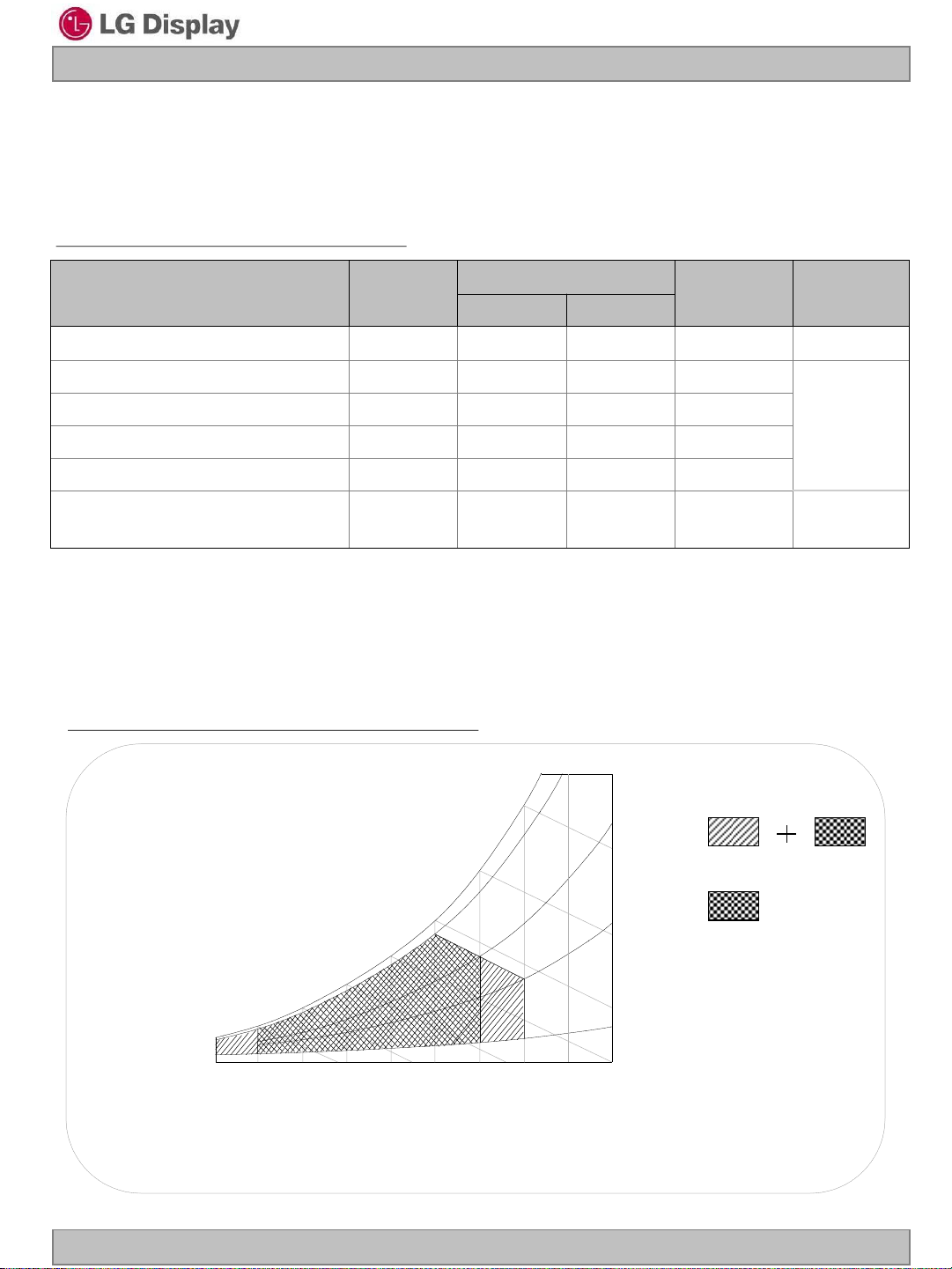
Note : 1. Temperature and relative humidity range are shown in the figure below.
Wet bulb temperature should be 39 °C Max, and no condensation of water.
2. Maximum Storage Humidity is up to 40℃, 90% RH only for 4 corner light leakage Mura.
3. Storage condition is guaranteed under packing condition
4. LCM Surface Temperature should be Min. 0℃ and Max. 65℃ under the VLCD=5.0V,
fV=60Hz, 25℃ ambient Temp. no humidity control and LED string current is typical value.
FIG. 2 Temperature and relative humidity
90%
60
50
Wet Bulb
Temperature [℃]
40
30
20
10
0
10 20 30 40 50 60 70 80 0 -20
Dry Bulb Temperature [℃]
Ver. 0.3 Mar. 28, 2013
60%
40%
10%
Storage
Operation
Humidity
[(%)RH]
5 / 30
Page 6
LM190E0A
Liquid Crystal Display
Product Specification
3. Electrical specifications
3-1. Electrical characteristics
It requires two power inputs. One is employed to power the LCD electronics and to drive the
TFT array and liquid crystal. The second input power for the LED/Backlight, is typically
generated by an LED Driver. The LED driver is an external unit to the LCDs.
Table 2. Electrical characteristics
Parameter Symbol
Values
Unit Notes
Min Typ Max
MODULE :
Power Supply Input Voltage V
Permissive Input Voltage Ripple V
I
Power Supply Input Current
LCD-MOSAIC
I
LCD-GREEN
Power Consumption P
Inrush current I
LCD
RF
LCD
RUSH
4.5 5.0 5.5 Vdc
- - 0.2 V 3
- 450 563 mA 1
- 600 750 mA 2
- 2.25 2.81 Watt 1
- - 3.0 A 4
Note :
1. The specified current and power consumption are under the VLCD=5.0V, 25 2°C,fV=60Hz
condition whereas mosaic pattern(8 x 6) is displayed and fV is the frame frequency.
2. The current is specified at the maximum current pattern.
3. Permissive power ripple should be measured under VLCD=5.0V, maximum frame rate (fV) at 25°C.
Additionally, we recommend the bandwidth configuration of oscilloscope is to be under 20MHz.
4. The duration of rush current is about 5ms and rising time of power Input is 500us 20%.
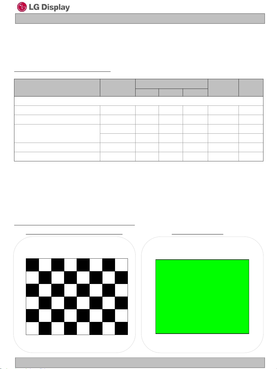
FIG.3 pattern for Electrical characteristics
power consumption measurement
power input ripple
White : 255Gray
Black : 0Gray
Mosaic Pattern(8 x 6)
Ver. 0.3 Mar. 28, 2013
Green 255
6 / 30
Page 7
Product Specification
Table 3. LED array ELECTRICAL CHARACTERISTICS
LM190E0A
Liquid Crystal Display
Parameter Symbol Condition
LED String Current Is - 100 105 mA 1,2,5
LED String Voltage Vs 42.8 45.8 48.8 V 1,5
Power
Consumption
LED Life Time LED_LT 30,000 - - Hrs 3
Notes) The LED Bar consists of 30 LED packages, 2 strings (parallel) x 15 packages (serial)
LED driver design guide
: The design of the LED driver must have specifications for the LED in LCD Assembly.
The performance of the LED in LCM, for example life time or brightness, is extremely
influenced by the characteristics of the LED driver.
So all the parameters of an LED driver should be carefully designed and output current
should be Constant current control.
Please control feedback current of each string individually to compensate the current
variation among the strings of LEDs.
When you design or order the LED driver, please make sure unwanted lighting caused by
the mismatch of the LED and the LED driver (no lighting, flicker, etc) never occurs.
When you confirm it, the LCD module should be operated in the same condition as
installed in your instrument.
Notes :
1. The specified values are for a single LED bar.
2. The specified current is defined as the input current for a single LED string with 100% duty cycle.
3. The LED life time is defined as the time when brightness of LED packages become 50% or less
than the initial value under the conditions at Ta = 25 2°C and LED string current is typical value.
4. The power consumption shown above does not include loss of external driver.
The typical power consumption is calculated as PBar = Vs(Typ.) x Is(Typ.) x No. of strings.
The maximum power consumption is calculated as PBar = Vs(Max.) x Is(Typ.) x No. of strings.
5. LED operating conditions must not exceed Max. ratings.
PBar 9.2 9.8 Watt 1,2,4
Min. Typ. Max.
Values
Unit
Note
s
Ver. 0.3 Mar. 28, 2013
7 / 30
Page 8
Product Specification
3-2. Interface connections
3-2-1. LCD Module
LCD connector(CN1) : IS100-L30O-C23(UJU), GT103-30S-H15 (LSM)
Mating connector : FI-X30H and FI-X30HL (JAE) or Equivalent
Table 4. Module connector(CN1) pin configuration
LM190E0A
Liquid Crystal Display
Pin No
1
2
3
4
5
6
7
8
9
10
11
12
13
14
15
16
17
18
19
20
21
22
23
24
25
26
27
28
29
30
Symbol Description
RXO0 RXO0+
RXO1 RXO1+
RXO2 RXO2+
GND
RXOC RXOC+
RXO3 RXO3+
RXE0 RXE0+
GND
RXE1 RXE1+
GND
RXE2 RXE2+
RXEC RXEC+
RXE3 RXE3+
GND
NC
NC
PWM_OUT
VLCD
VLCD
VLCD
Minus signal of 1st channel 0 (LVDS)
Plus signal of 1st channel 0 (LVDS)
Minus signal of 1st channel 1 (LVDS)
Plus signal of 1st channel 1 (LVDS)
Minus signal of 1st channel 2 (LVDS)
Plus signal of 1st channel 2 (LVDS)
Ground
Minus signal of 1st clock channel (LVDS)
Plus signal of 1st clock channel (LVDS)
Minus signal of 1st channel 3 (LVDS)
Plus signal of 1st channel 3 (LVDS)
Minus signal of 2nd channel 0 (LVDS)
Plus signal of 2nd channel 0 (LVDS)
Ground
Minus signal of 2nd channel 1 (LVDS)
Plus signal of 2nd channel 1 (LVDS)
Ground
Minus signal of 2nd channel 2 (LVDS)
Plus signal of 2nd channel 2 (LVDS)
Minus signal of 2nd clock channel (LVDS)
Plus signal of 2nd clock channel (LVDS)
Minus signal of 2nd channel 3 (LVDS)
Plus signal of 2nd channel 3 (LVDS)
Ground
No Connection (I2C Serial interface for LCM)
No Connection (I2C Serial interface for LCM)
For Control Burst frequency of Inverter
Power Supply (5.0V)
Power Supply (5.0V)
Power Supply (5.0V)
First Pixel data
Second Pixel data
Ver. 0.3 Mar. 28, 2013
8 / 30
Page 9
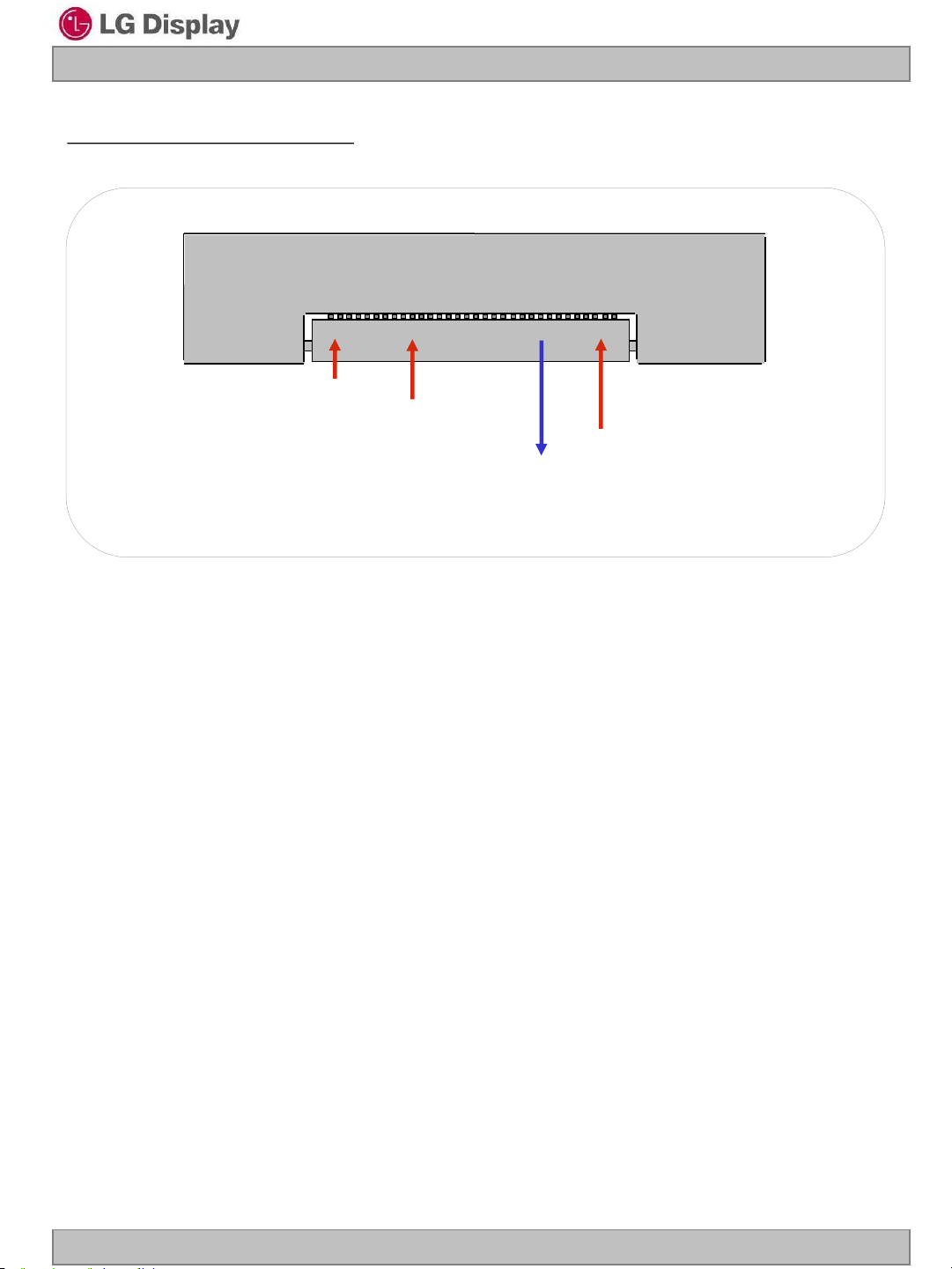
FIG. 4 Connector diagram
#
1
#1 #30
1’st signal pairs
LM190E0A
Liquid Crystal Display
Product Specification
IS100-L30O-C23(UJU)
#30
2’nd signal pairs
Power(+5V)
PWM_OUT
Rear view of LCM
Note:
1. NC: No Connection.
2. All GND(ground) pins should be connected together and to Vss which should also
be connected to the LCD’s metal frame.
3. 3. All V
(power input) pins should be connected together.
LCD
4. Input Level of LVDS signal is based on the IEA 664 Standard.
5. PWM_OUT is a reference signal for LED Driver control.
This PWM signal is synchronized with vertical frequency.
Its frequency is 6 times of vertical frequency, and its duty ratio is 50%.
If the system don’t use this pin, do not connect.
Ver. 0.3 Mar. 28, 2013
9 / 30
Page 10
LM190E0A
Liquid Crystal Display
Product Specification
3-2-2. BACKLIGHT CONNECTOR PIN CONFIGURATION(CN3)
The LED interface connector is a model SM06B-SHJH(HF) wire-locking type manufactured by JST.
The mating connector is a SHJP-06V-S(HF) or SHJP-06V-A-K(HF) and Equivalent.
The pin configuration for the connector is shown in the table below.
Table 5. LED connector pin configuration
Pin Symbol Description Notes
1 FB1 Channel1 Current Feedback
2 NC No connection
3 VLED LED Power Supply
4 VLED LED Power Supply
5 NC No connection
6 FB2 Channel2 Current Feedback
#1
Rear view of LCM
#6
[ Figure 5 ] Backlight connector view
Ver. 0.3 Mar. 28, 2013
10 / 30
Page 11
3-3. LVDS characteristics
3-3-1. DC Specification
LVDS -
LVDS +
LM190E0A
Liquid Crystal Display
Product Specification
|VID|
# |VID| = |(LVDS+) – (LVDS-)|
# VCM = {(LVDS+) + (LVDS-)}/2
0V
V
CM
V
IN_MAXVIN_MIN
Description Symbol Min Max Unit Notes
LVDS Differential Voltage |VID| 200 600 mV -
LVDS Common mode Voltage V
LVDS Input Voltage Range V
CM
IN
0.6 1.8 V -
0.3 2.1 V -
3-3-2. AC Specification
T
clk
LVDS Clock
LVDS Data
SKEW
clk
t
( F
1 ) 85 MHz > Fclk ≥ 65 MHz : - 400 ~ + 400
t
SKEW
2 ) 65 MHz > Fclk ≥ 25 MHz : - 600 ~ + 600
< Clock skew margin between channel >
= 1 / T
clk
)
Description Symbol Min Max Unit Notes
LVDS Clock to Data Skew Margin
LVDS Clock to Clock Skew Margin
(Even to Odd)
Maximum deviation
of input clock frequency during SSC
Maximum modulation frequency
of input clock during SSC
t
SKEW
t
SKEW
t
SKEW_EO
F
DEV
F
MOD
- 400 + 400 ps
- 600 + 600 ps
- 1/7 + 1/7 T
- ± 3 % -
- 200 KHz -
85MHz > Fclk ≥ 65MHz
65MHz > Fclk ≥ 25MHz
clk
-
Note :
This SSC specification is based on T-CON operation. According to various system, the
condition for optimum SSC can be varied. We recommend the SSC condition should be
adjusted in order to prevent any kinds of failure symptoms.
Ver. 0.3 Mar. 28, 2013
11 / 30
Page 12

Product Specification
t
SKEW_EO
LM190E0A
Liquid Crystal Display
LVDS Odd Clock
LVDS Even Clock
LVDS Even Data
< Clock skew margin between clock (Even/Odd) >
3-3-3. LVDS Data format
RCLK +
RXinO 0 +/ -
RXinO 1 +/ -
RXinO 2 +/ -
RXinO 3 +/ -
RXinE 0 +/ -
RXinE 1 +/ -
RXinE 2 +/ -
OR 3 OR 2 OR 1 OR 0
OG 4 OG 3 OG 2 OG 1
OB 5 OB 4 OB 3 OB 2
OG 7 OG 6 OR 7 OR 6
ER 3 ER 2 ER 1 ER 0
EG 4 EG 3 EG 2 EG 1
EB 5 EB 4 EB 3 EB 2
Tclk * 4 / 7 Tclk * 3 / 7
Tclk * 1 / 7
OG 0 OR 5 OR 4 OR 3 OR 2 OR 1 OR 0
OB 1 OB 0 OG 5 OG 4 OG 3 OG 2 OG 1
DE
EG 0 ER 5 ER 4 ER 3 ER 2 ER 1 ER 0
EB 1 EB 0 EG 5 EG 4 EG 3 EG 2 EG 1
DE
T
clk
T
clk
Tclk
VSYNC HSYNC
X OB 7 OB 6 OG 7 OG 6 OR 7 OR 6
VSYNC HSYNC
OB 5 OB 4 OB 3 OB 2
EB 5 EB 4 EB 3 EB 2
OG 0 OR 5 OR 4
OB 1 OB 0 OG 5
VSYNC HSYNC
DE
X OB 7 OB 6
EG 0 ER 5 ER 4
EB 1 EB 0 EG 5
VSYNC HSYNC
DE
MSB R 7
R 6
R 5
R 4
R 3
R 2
R 1
R 0 LSB
* ODD = 1 st Pixel
EVEN = 2 nd Pixel
RXinE 3 +/ -
EG 7 EG 6 ER 7 ER 6
X EB 7 EB 6 EG 7 EG 6 ER 7 ER 6
Current ( Nth ) Cycle Previous ( N - 1 ) th Cycle Next ( N + 1 )
< LVDS Data Format >
Ver. 0.3 Mar. 28, 2013
X EB 7 EB 6
th Cycle
12 / 30
Page 13

LM190E0A
Liquid Crystal Display
Product Specification
Table 6. Required signal assignment for Flat Link(NS:DS90CF383) transmitter
Pin # Require Signal Pin Name Pin # Require Signal Pin Name
1 Power Supply for TTL Input VCC 29 Ground pin for TTL GND
2 TTL Input (R7) D5 30 TTL Input (DE) D26
3 TTL Input (R5) D6 31 TTL Level clock Input TX CLKIN
4 TTL Input (G0) D7 32 Power Down Input PWR DWN
5 Ground pin for TTL GND 33 Ground pin for PLL PLL GND
6 TTL Input (G1) D8 34 Power Supply for PLL PLL VCC
7 TTL Input (G2) D9 35 Ground pin for PLL PLL GND
8 TTL Input (G6) D10 36 Ground pin for LVDS LVDS GND
9 Power Supply for TTL Input VCC 37 Positive LVDS differential data output 3
10 TTL Input (G7) D11 38 Negative LVDS differential data output 3
11 TTL Input (G3) D12 39 Positive LVDS differential clock output
12 TTL Input (G4) D13 40 Negative LVDS differential clock output
13 Ground pin for TTL GND 41 Positive LVDS differential data output 2
14 TTL Input (G5) D14 42 Negative LVDS differential data output 2
15 TTL Input (B0) D15 43 Ground pin for LVDS LVDS GND
16 TTL Input (B6) D16 44 Power Supply for LVDS LVDS VCC
17 Power Supply for TTL Input VCC 45 Positive LVDS differential data output 1
18 TTL Input (B7) D17
19 TTL Input (B1) D18
20 TTL Input (B2) D19
22 TTL Input (B3) D20
23 TTL Input (B4) D21
24 TTL Input (B5) D22
25 TTL Input (RSVD) D23
46 Negative LVDS differential data output 1
47 Positive LVDS differential data output 0
48 Negative LVDS differential data output 0
49 Ground pin for LVDS LVDS GND 21 Ground pin for TTL Input GND
50 TTL Input (R6) D27
51 TTL Input (R0) D0
52 TTL Input (R1) D1
53 Ground pin for TTL GND
TxOUT3+
TxOUT3-
TX CLKOUT+
TX CLKOUT-
TX OUT2+
TX OUT2-
TX OUT1+
TX OUT1-
TX OUT0+
TX OUT0-
26 Power Supply for TTL Input VCC 54 TTL Input (R2) D2
55 TTL Input (R3) D3 27 TTL Input (HSYNC) D24
56 TTL Input (R4) D4 28 TTL Input (VSYNC) D25
Notes : 1. Refer to LVDS Transmitter Data Sheet for detail descriptions.
2. 7 means MSB and 0 means LSB at R,G,B pixel data
Ver. 0.3 Mar. 28, 2013
13 / 30
Page 14

LM190E0A
Liquid Crystal Display
Product Specification
3-4. Signal timing specifications
This is the signal timing required at the input of the User connector. All of the interface signal
timing should be satisfied with the following specifications for it’s proper operation.
Table 7. Timing table
D
CLK
Horizontal
Vertical
Parameter Symbol Min. Typ. Max.
Period t
Frequency f
Horizontal Valid
H Period Total
Horizontal Blank
Hsync Frequency
Width
Horizontal Back
Porch
Horizontal Front
Porch
Vertical Valid t
V Period Total t
Vertical Blank t
Vsync Frequency f
Width t
Vertical Back
Porch
Vertical Front
Porch
CLK
CLK
t
HV
t
HP
t
HB
f
H
t
WH
t
HBP
t
HFP
VV
VP
VB
V
VVV
t
VBP
t
VFP
14.8 18.5 22.2 ns
45.0 54.0 67.5 MHz
640 640 640
704 844 960
64 204 320
53.3 64.0 80.0 kHz
16 56 80
32 124 200
16 24 40
1024 1024 1024
1032 1066 1536
8 42 512
50 60 75 Hz
2 3 250
5 38 250
1 1 12
Unit Notes
Pixel frequency
: Typ.108MHz
t
t
t
t
CLK
CLK
HP
HP
Note: Hsync period and Hsync width-active should be even number times of tCLK. If the value is odd number
times of tCLK, display control signal can be asynchronous. In order to operate this LCM a Hsync,
Vsyn, and DE(data enable) signals should be used.
1. The performance of the electro-optical characteristics may be influenced by variance of the vertical
refresh rates.
2. Vsync and Hsync should be keep the above specification.
3. Hsync Period, Hsync Width, and Horizontal Back Porch should be any times of of character
number(4).
4. The polarity of Hsync, Vsync is not restricted.
5. The Max frequency of 1280X1024 resolution is 67.5Mhz
Ver. 0.3 Mar. 28, 2013
14 / 30
Page 15

Product Specification
3-5. Signal timing waveforms
1. DCLK , DE, DATA waveforms
t
CLK
Dclk
Invalid
Data
DE(Data Enable)
t
SD
t
SI
t
HD
Valid
LM190E0A
Liquid Crystal Display
Invalid
t
HI
2. Horizontal waveform
DE(Data Enable)
3. Vertical waveform
DE(Data Enable)
tHV
tVV
tHP
t
DE
VP
DE
Ver. 0.3 Mar. 28, 2013
15 / 30
Page 16

LM190E0A
Liquid Crystal Display
Product Specification
3-6. Color input data reference
The brightness of each primary color (red,green and blue) is based on the 8bit gray scale data
input for the color ; the higher the binary input, the brighter the color. The table below
provides a reference for color versus data input.
Table 8. Color data reference
Input Color Data
Color
Red
MSB LSB
R7 R6 R5 R4 R3 R2 R1 R0 G7 G6 G5 G4 G3 G2 G1 G0 B7 B6 B5 B4 B3 B2 B1 B0
MSB LSB
Green
Blue
MSB LSB
Basic
Color
Red
Green
Blue
Black
Red (255)
Green (255)
Blue (255)
Cyan
Magenta
Yellow
White
Red(000) Dark
Red(001)
Red(002)
- - - - - - - - -
- - - - - - - - Red(253)
Red(254)
Red(255) Bright
Green(000) Dark
Green(001)
Green(002)
- - - - - - - - -
- - - - - - - - Green(253)
Green(254)
Green(255)Bright
Blue(000) Dark
Blue(001)
Blue(002)
- - - - - - - - -
- - - - - - - - Blue(253)
Blue(254)
Blue(255) Bright
0
1
0
0
0
1
1
1
0
0
0
-
-
1
1
1
0
0
0
-
0
0
0
0
0
0
-
0
0
0
0
1
0
0
0
1
1
1
0
0
0
-
-
1
1
1
0
0
0
-
0
0
0
0
0
0
-
0
0
0
0
1
0
0
0
1
1
1
0
0
0
-
-
1
1
1
0
0
0
-
0
0
0
0
0
0
-
0
0
0
0
1
0
0
0
1
1
1
0
0
0
-
-
1
1
1
0
0
0
-
0
0
0
0
0
0
-
0
0
0
0
1
0
0
0
1
1
1
0
0
0
-
-
1
1
1
0
0
0
-
0
0
0
0
0
0
-
0
0
0
0
1
0
0
0
1
1
1
0
0
0
-
-
1
1
1
0
0
0
-
0
0
0
0
0
0
-
0
0
0
0
1
0
0
0
1
1
1
0
0
1
-
-
0
1
1
0
0
0
-
0
0
0
0
0
0
-
0
0
0
0
1
0
0
0
1
1
1
0
1
0
-
-
1
0
1
0
0
0
-
0
0
0
0
0
0
-
0
0
0
0
0
1
0
1
0
1
1
0
0
0
-
-
0
0
0
0
0
0
-
1
1
1
0
0
0
-
0
0
0
0
0
1
0
1
0
1
1
0
0
0
-
-
0
0
0
0
0
0
-
1
1
1
0
0
0
-
0
0
0
0
0
1
0
1
0
1
1
0
0
0
-
-
0
0
0
0
0
0
-
1
1
1
0
0
0
-
0
0
0
0
0
1
0
1
0
1
1
0
0
0
-
-
0
0
0
0
0
0
-
1
1
1
0
0
0
-
0
0
0
0
0
1
0
1
0
1
1
0
0
0
-
-
0
0
0
0
0
0
-
1
1
1
0
0
0
-
0
0
0
0
0
1
0
1
0
1
1
0
0
0
-
-
0
0
0
0
0
0
-
1
1
1
0
0
0
-
0
0
0
0
0
1
0
1
0
1
1
0
0
0
-
-
0
0
0
0
0
1
-
0
1
1
0
0
0
-
0
0
0
0
0
1
0
1
0
1
1
0
0
0
-
-
0
0
0
0
1
0
-
1
0
1
0
0
0
-
0
0
0
0
0
0
1
1
1
0
1
0
0
0
-
-
0
0
0
0
0
0
-
0
0
0
0
0
0
-
1
1
1
0
0
0
1
1
1
0
1
0
0
0
-
-
0
0
0
0
0
0
-
0
0
0
0
0
0
-
1
1
1
0
0
0
1
1
1
0
1
0
0
0
-
-
0
0
0
0
0
0
-
0
0
0
0
0
0
-
1
1
1
0
0
0
1
1
1
0
1
0
0
0
-
-
0
0
0
0
0
0
-
0
0
0
0
0
0
-
1
1
1
0
0
0
1
1
1
0
1
0
0
0
-
-
0
0
0
0
0
0
-
0
0
0
0
0
0
-
1
1
1
0
0
0
1
1
1
0
1
0
0
0
-
-
0
0
0
0
0
0
-
0
0
0
0
0
0
-
1
1
1
0
0
0
1
1
1
0
1
0
0
0
-
-
0
0
0
0
0
0
-
0
0
0
0
0
1
-
0
1
1
0
0
0
1
1
1
0
1
0
0
0
-
-
0
0
0
0
0
0
-
0
0
0
0
1
0
-
1
0
1
Ver. 0.3 Mar. 28, 2013
16 / 30
Page 17

3-7. Power sequence
LM190E0A
Liquid Crystal Display
Product Specification
90% 90%
VLCD
Power Supply For LCD
0V
Interface Signal (Tx)
0V
Power for LED
Table 9. Power sequence
Parameter
T1 0.5 - 10 ms
T2 0.01 - 50 ms
T3 500 - - ms
10%
T2 T5 T7
T1
Valid data
T3
OFF
Min Typ Max
LED on
Values
T4
OFF
10%
Units
T4 200 - - ms
T5 0.01 - 50 ms
T7 1 - - s
Notes :
1. Please V
power on only after connecting interface cable to LCD.
LCD
2. Please avoid floating state of interface signal at invalid period.
3. When the interface signal is invalid, be sure to pull down the power supply for
LCD V
to 0V.
LCD
4. LED power must be turn on after power supply for LCD an interface signal are valid.
Ver. 0.3 Mar. 28, 2013
17 / 30
Page 18

Product Specification
LM190E0A
Liquid Crystal Display
3-8. V
Power dip condition
LCD
FIG. 6 Power dip condition
1) Dip condition
3.5V ≤V
< 4.5V , td≤20ms
LCD
2) V
< 3.5V
LCD
V
-dip conditions should also follow the Power On/Off conditions for supply voltage.
LCD
td
V
LCD
4.5V
3.5V
GND(ground)
Ver. 0.3 Mar. 28, 2013
18 / 30
Page 19

LM190E0A
Liquid Crystal Display
Product Specification
4. Optical specification
Optical characteristics are determined after the unit has been ‘ON’ for 30 minutes in a dark
environment at 25°C.
Table 10. Optical characteristics
Parameter Symbol
Ta= 25°C, V
Min Typ Max
Contrast Ratio CR 700 1000 -
Surface Luminance, white L
Surface Luminance, Black L
Luminance Variation
Response Time
Gray To Gray T
Gray-to-Gray (BW) G to G
WHITE
GTG_AVR
WH
BL
9P 75 - - %
BW
200 250 - cd/m
- - 0.6 cd/m2
- 14 25
- 8 -
Color Gamut 67.5 72 - % (PR-650)
RED
GREEN
Color Coordinates
[CIE1931]
BLUE
WHITE
Rx
Ry 0.335
Gx 0.321
Gy 0.607
Bx 0.151
Typ
-0.03
By 0.062
Wx 0.313
Wy 0.329
Viewing Angle (CR>10)
General
Horizontal H 170 178
Vertical V 170 178
Crosstalk 1.5 %
Gamma
Luminance uniformity Angular dependence
LR - - 1.73
(TCO 5.1)
Color grayscale linearity Δu’v’ 0.018
Color uniformity
Angular dependence( TCO 5.1)
- -
=5.0V, fV=60Hz f
LCD
Values
0.654
2.2
Typ
+0.03
0.025
=54.0MHz, IBL=100mA
CLK
Units Notes
(PR-880)
2
2
(PR-880)
(PR-880)
(PR-880)
ms
Ms
(RD-80S)
(PR-650)
(PR-880)
(PR-880)
(PR-880)
(PR-650)
(PR-880)
1
2
3
4
5
6
7
8
9
Ver. 0.3 Mar. 28, 2013
19 / 30
Page 20
LM190E0A
Liquid Crystal Display
Product Specification
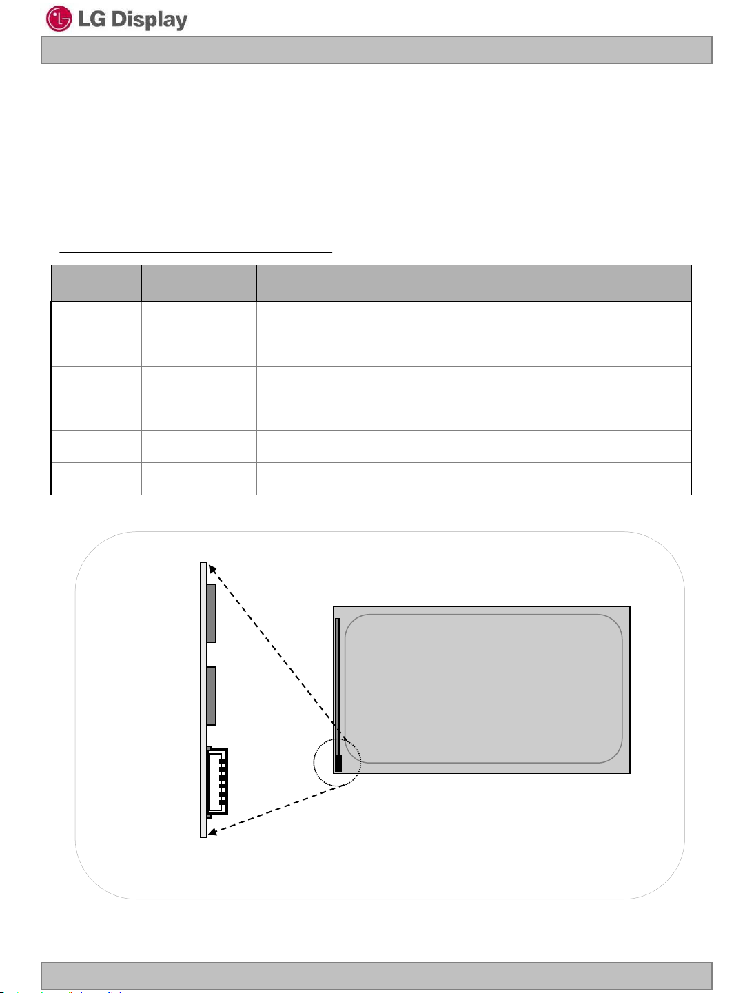
The values specified are at an approximate distance 50cm from the LCD surface at a viewing
angle of and equal to 0 °.
FIG. 7 presents additional information concerning the measurement equipment and method.
FIG. 7 Optical characteristic measurement equipment and method
Optical
LCD Module
Stage(x,y)
Pritchard 880
or equivalent
50cm
Notes :
1. Contrast ratio(CR) is defined mathematically as :It is measured at center point(1)
Surface luminance with all white pixels
Contrast ratio = ---------------------------------------------------------
Surface luminance with all black pixels
2. Surface luminance is the luminance value at center 1 point(1) across
the LCD surface 50cm from the surface with all pixels displaying white.
For more information see FIG 8.
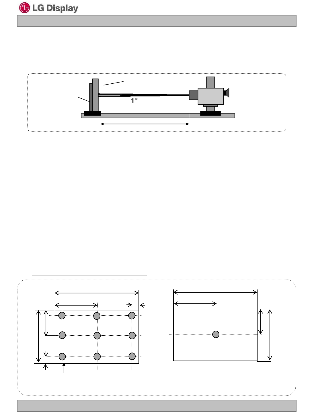
3. The variation in surface luminance ,
is defined as
WHITE
Minimum (P1,P2 …..P9)
Maximum (P1,P2 …..P9)
= --------------------------------------------- *100
WHITE
For more information see Figure 8.
FIG. 8 Luminance measuring point
<Measuring point for luminance variation> <Measuring point for surface luminance>
V
V/2
V/10
Active Area
H
H/2
3
5 6
7
1
8
H/10
4 2
H : 376.320 mm
H/2
9
H
V/2
V : 301.056 mm
@ H,V : Active Area
Ver. 0.3 Mar. 28, 2013
V
20 / 30
Page 21

LM190E0A
Liquid Crystal Display
Product Specification
Notes :
4. Response time is the time required for the display to transition from black to white
(Decay Time, TrD) and from white to black (Rise Time, TrR)
The sampling rate is 2,500 sample/sec. For additional information see FIG. 9.
The response time is defined as the following figure and shall be measured by
switching the input signal for each gray to gray.
FIG. 9 Response time (measurement equipment : RD-80S)
TrR TrD
100
90
Optical
white black white
response
[%]
10
0
The Gray to Gray response time is defined as the following figure and shall be measured by
switching the input signal for “Gray To Gray “.
- Gray step : 5 Step
- TGTG_AVR is the total average time at rising time and falling time for “Gray To Gray “.
- if system use ODC ( Over Driving Circuit) function, Gray to Gary response time may be
5ms~8ms GtG
* it depends on Overshoot rate.
Table. 11 GTG Gray Table
Gray to Gray
G255 G191 G127 G63 G0
Falling Time G255
Rising Time
G191
G127
G63
G0
Ver. 0.3 Mar. 28, 2013
21 / 30
Page 22

LM190E0A
Liquid Crystal Display
Product Specification
Notes :
5. Viewing angle is the angle at which the contrast ratio is greater than 10 or 5. The angles are
determined for the horizontal or x axis and the vertical or y axis with respect to the z axis
which is normal to the LCD surface. For more information see FIG. 10 .
FIG. 10 Viewing angle
<Dimension of viewing angle range>
= 180, Left
= 270, Down
6. Crosstalk
The equation of crosstalk : (L
(L
A[or C]2-LA[or C]1
B[or D]2-LB[or D]1
For more information see Figure 11.
FIG. 11 Crosstalk Measuring Point
Normal
E
Y
= 90, Up
= 0, Right
/L
/L
) 100(%) [Vertical],
A[or C]1
) 100(%) [Horizontal]
B[or D]1
Pattern 1
(Half gray: gray 127)
A/2
LA1
A/8
B/8
(Background: gray 127, Rectangular: gray 255 )
B
LB1
LD1
B/2
LC1
A
Ver. 0.3 Mar. 28, 2013
Pattern 2
A/4 A/2 A/4
LA2
LB2
LD2
LC2
B/4
B/2
B/4
22 / 30
Page 23

Liquid Crystal Display
Product Specification
Notes :
7. Luminance Uniformity - angular – dependence (LR& TB)
TCO 5.0 Luminance uniformity – angular dependence, is the capacity of the VDU
to present the same Luminance level independently of the viewing direction.
The angular-dependent luminance uniformity is calculated as the ratio of maximum
luminance to minimum luminance in the specified measurement areas.
- Test pattern : Full white 4˚× 4˚square size, back ground shall be set to 80%
image loading, RGB 204, 204, 204
- Test luminance : ≥150cd/㎡
- Test point : 5-point
- Test distance : D * 1.5 = 72.0㎝
- Test method : LR = ((L
TB = ((L
max.+30deg.
max.+15deg.
/ L
min. +30deg.
/ L
min. +15deg.
) + (L
)
max. -30deg.
/ L
min. -30deg.
)) / 2
LM190E0A
FIG. 12 Luminance Uniformity angular dependence
< Luminance uniformity - angular dependence measuring point >
H
H/10
H/10
V/10
V/2
D
V/10
H/2
V
Ver. 0.3 Mar. 28, 2013
23 / 31
Page 24

LM190E0A
Liquid Crystal Display
Product Specification
Notes :
8. Color grayscale linearity , Δu’v’ is defined as
22
)''()''( BABA vvuu
Where indices A and B are the two gray levels found to have the largest color differences
between them.
i.e. get the largest Δu’ and Δv’ of each 6pairs of u’ and v’ and calculate Δu’v’ .
-Test pattern : 100% full white pattern with a test pattern as shown FIG.12
Squares of 40mm by 40mm in size, filled with 255, 225, 195, 165, 135 and 105
grayscale steps should be arranged in the center of the screen.
-Test method
First gray step : move a square of 255 gray level should be moved into the center of the screen
and measure luminance and u’ and v’ coordinates.
Next gray step : move a 255 gray square into the center and measure both luminance and
u’ and v’ coordinates.
The same procedure shall then be repeated for gray steps 195, 165, 135 and 105.
FIG. 13 Color grayscale linearity
40mm
40mm
Ver. 0.3 Mar. 28, 2013
24 / 31
Page 25

Liquid Crystal Display
Product Specification
Notes :
9. Colour uniformity Angular dependence (LR)
TCO 5.1 Color uniformity – angular dependence, is the capacity of the VDU
to present the same Colour level independently of the viewing direction.
The angular-dependent colour uniformity is calculated as the largest difference in
△u'v' value
- Test pattern : Full white 4˚× 4˚square size, back ground shall be set to 80%
image loading, RGB 204, 204, 204
- Test luminance : ≥200cd/㎡
- Test point : 3-point
- Test distance : D * 1.5
- Test method
1. The screen shall then be rotated ±30 degrees around a vertical axis through
the screen centre-point and the chromaticity co-ordinates at positions PL, PR,
(u'
PL/ ± 30º
2. △u’v’ shall be calculated for each measured position using the formula
a. △u’v’
b. △u’v
3. The largest difference in △ u'v' value shall be reported
+30º
-30º
, v'
=((u'
=((u'
PL/ ± 30º
PL/ + 30º
PL/ - 30º
and u'
- u'
- u'
PR/ ± 30º
PR/ + 30º
PR/ - 30º
, v'
PR/ ± 30º
)2+(v'
)2+(v'
respectively) shall be recorded.
PL/ + 30º
PL/ - 30º
- v'
- v'
PR/ -30º
PR/ +30º
)2)^
)2)^
1/2
1/2
LM190E0A
FIG. 14 Colour uniformity Angular dependence
< Colour uniformity - angular dependence measuring point >
H
H/10
H/10
V/2
P
L
P
D
C
P
R
H/2
V
Ver. 0.3 Mar. 28, 2013
25 / 31
Page 26

Table 12. Gray Scale Specification
Gray Level Relative Luminance [%] (Typ.)
LM190E0A
Liquid Crystal Display
Product Specification
0
15
31
47
63
79
95
111
127
143
159
175
191
207
223
0.1
0.3
1.08
2.5
4.72
7.7
11.49
16.2
21.66
28.2
35.45
43.8
53.00
63.3
74.48
239
255
Ver. 0.3 Mar. 28, 2013
86.8
100
26 / 31
Page 27

LM190E0A
Liquid Crystal Display
Product Specification
5. Mechanical characteristics
The contents provide general mechanical characteristics. In addition the figures in the next
page are detailed mechanical drawing of the LCD.
Table 13. Mechanical characteristics
Horizontal 396.0 mm
Outline dimension
Bezel area
Active display area
Weight 1705g (Typ.) 1790g (Max)
Surface treatment
Notes : Please refer to a mechanic drawing in terms of tolerance at the next page.
Vertical 324.0 mm
Depth 9.9mm
Horizontal 378.8 mm
Vertical 303.0 mm
Horizontal 374.784 mm
Vertical 299.827 mm
Hard coating(3H)
Anti-glare treatment of the front polarizer
Ver. 0.3 Mar. 28, 2013
27 / 30
Page 28

<FRONT VIEW>
LM190E0A
Liquid Crystal Display
Product Specification
Ver. 0.3 Mar. 28, 2013
28 / 30
Page 29

<REAR VIEW>
LM190E0A
Liquid Crystal Display
Product Specification
Ver. 0.3 Mar. 28, 2013
29 / 30 29 / 30
Page 30

Product Specification
6. Reliability
Table 13. Environment test conditions
No Test Item Condition
LM190E0A
Liquid Crystal Display
1 High temperature storage test
2 Low temperature storage test
3 High temperature operation test
4 Low temperature operation test
5
6
7 Humidity condition Operation
8
Vibration test
(non-operating)
Shock test
(non-operating)
Altitude
operating
storage / shipment
Ta= 60°C 240h
Ta= -20°C 240h
Ta= 50°C 50%RH 240h
Ta= 0°C 240h
Wave form : random
Vibration level : 1.00G RMS
Bandwidth : 10-300Hz
Duration : X, Y, Z, 10 min
One time each direction
Shock level : 100G
Waveform : half sine wave, 2ms
Direction : ±X, ±Y, ±Z
One time each direction
Ta= 40 °C ,90%RH
0 - 16,400 feet(5,000m)
0 - 40,000 feet(12,192m)
9
{ Result evaluation criteria }
There should be no change which might affect the practical display function when the display
quality test is conducted under normal operating condition.
Ver. 0.3 Mar. 28, 2013
Maximum Storage Humidity for
4 corner light leakage Mura.
Max 70%RH , Ta=40℃
30 / 30
Page 31

Product Specification
7. International standards
7-1. Safety
a) UL 60950-1, Underwriters Laboratories Inc.
Information Technology Equipment - Safety - Part 1 : General Requirements.
b) CAN/CSA C22.2 No.60950-1-07, Canadian Standards Association.
Information Technology Equipment - Safety - Part 1 : General Requirements.
c) EN 60950-1, European Committee for Electrotechnical Standardization (CENELEC).
Information Technology Equipment - Safety - Part 1 : General Requirements.
d) IEC 60950-1, The International Electrotechnical Commission (IEC).
Information Technology Equipment - Safety - Part 1 : General Requirements.
LM190E0A
Liquid Crystal Display
7-2. EMC
a) ANSI C63.4 “American National Standard for Methods of Measurement of Radio-Noise
Emissions from Low-Voltage Electrical and Electronic Equipment in the Range of
9 kHz to 40 GHz.”
American National Standards Institute (ANSI), 2003.
b) CISPR 22 “Information technology equipment – Radio disturbance characteristics –
Limit and methods of measurement." International Special Committee on Radio
Interference (CISPR), 2005.
c) CISPR 13 “Sound and television broadcast receivers and associated equipment –
Radio disturbance characteristics – Limits and method of measurement.”
International Special Committee on Radio Interference (CISPR), 2006.
7-3. Environment
a) RoHS, Directive 2011/65/EU of the European Parliament and of the council of 8 June 2011
Ver. 0.3 Mar. 28, 2013
31 / 30
Page 32

Product Specification
8. Packing
8-1. Designation of lot mark
a) Lot mark
A B C D E F G H I J K L M
A,B,C : Size (Inch) D : Year
E : Month F ~ M : Serial No.
Note:
1. Year
LM190E0A
Liquid Crystal Display
Year
Mark
2013 2012 2011
2014 E 2015
C B A
D
2016 G 2017 H 2018 J 2019
F
2020
K
2. Month
A
Nov
B
Month
Mark
Apr 5 May
4
Jun 7 Jul 8 Aug 9 Sep
6
Oct
b) Location of lot mark
Serial No. is printed on the label. The label is attached to the backside of the LCD module.
This is subject to change without prior notice.
8-2. Packing form
a) Package quantity in one box : 14 pcs (2 Module is packed in 1 Bag)
b) Box size : 418(L)*365(W)*492(H)
Dec Mar Feb Jan
C 3 2 1
Ver. 0.3 Mar. 28, 2013
32 / 30
Page 33

LM190E0A
Liquid Crystal Display
Product Specification
9. Precautions
Please pay attention to the followings when you use this TFT LCD module.
9-1. Mounting Precautions
(1) You must mount a module using holes arranged in left & right sides.
(2) You should consider the mounting structure so that uneven force (ex. Twisted stress) is
not applied to the Module. And the case on which a module is mounted should have
sufficient strength so that external force is not transmitted directly to the module.
(3) Please attach the surface transparent protective plate to the surface in order to protect
the polarizer. Transparent protective plate should have sufficient strength in order to the
resist external force.
(4) You should adopt radiation structure to satisfy the temperature specification.
(5) Acetic acid type and chlorine type materials for the cover case are not desirable because
the former generates corrosive gas of attacking the polarizer at high temperature and the
latter causes circuit break by electro-chemical reaction.
(6) Do not touch, push or rub the exposed polarizers with glass, tweezers or anything harder
than HB pencil lead. And please do not rub with dust clothes with chemical treatment.
Do not touch the surface of polarizer for bare hand or greasy cloth.
(Some cosmetics are detrimental to the polarizer.)
(7) When the surface becomes dusty, please wipe gently with absorbent cotton or other soft
materials like chamois soaks with petroleum benzene. Normal-hexane is recommended
for cleaning the adhesives used to attach front / rear polarizers. Do not use acetone,
toluene and alcohol because they cause chemical damage to the polarizer.
(8) Wipe off saliva or water drops as soon as possible. Their long time contact with polarizer
causes deformations and color fading.
(9) Do not open the case because inside circuits do not have sufficient strength.
9-2. Operating precautions
(1) The spike noise causes the mis-operation of circuits. It should be lower than following
voltage : V=±200mV(Over and under shoot voltage)
(2) Response time depends on the temperature.(In lower temperature, it becomes longer.)
(3) Brightness depends on the temperature. (In higher temperature, it becomes lower.)
And in lower temperature, response time(required time that brightness is stable after
turned on) becomes longer.
(4) Be careful for condensation at sudden temperature change. Condensation makes damage
to polarizer or electrical contacted parts. And after fading condensation, smear or spot will
occur.
(5) When fixed patterns are displayed for a long time, remnant image is likely to occur.
(6) Module has high frequency circuits. Sufficient suppression to the electromagnetic
interference shall be done by system manufacturers. Grounding and shielding methods
may be important to minimized the interference.
(7) Please do not give any mechanical and/or acoustical impact to LCM. Otherwise, LCM can
not be operated its full characteristics perfectly.
(8) A screw which is fastened up the steels should be a machine screw (if not, it causes metal
foreign material and deal LCM a fatal blow)
(9) Please do not set LCD on its edge.
(10)Please conduct image sticking test after 2-hour aging with Full white or Rolling PTN
and normal temperature (25~40℃)
Ver. 0.3 Mar. 28, 2013
33 / 30
Page 34
LM190E0A
Liquid Crystal Display
Product Specification
9-3. Electrostatic discharge control
Since a module is composed of electronic circuits, it is not strong to electrostatic discharge.
Make certain that treatment persons are connected to ground through wrist band etc. And
don’t touch interface pin directly.
9-4. Precautions for strong light exposure
Strong light exposure causes degradation of polarizer and color filter.
9-5. Storage
When storing modules as spares for a long time, the following precautions are necessary.
(1) Store them in a dark place. Do not expose the module to sunlight or fluorescent light. Keep
the temperature between 5°C and 35°C at normal humidity.
(2) The polarizer surface should not come in contact with any other object.
It is recommended that they be stored in the container in which they were shipped.
9-6. Handling precautions for protection film
(1) The protection film is attached to the bezel with a small masking tape.
When the protection film is peeled off, static electricity is generated between
the film and polarizer. This should be peeled off slowly and carefully by people who are
electrically grounded and with well ion-blown equipment or in such a condition, etc.
(2) When the module with protection film attached is stored for a long time,
sometimes there remains a very small amount of glue still on the bezel
after the protection film is peeled off.
(3) You can remove the glue easily. When the glue remains on the bezel surface or
its vestige is recognized, please wipe them off with absorbent cotton waste or
other soft material like chamois soaked with normal-hexane.
Ver. 0.3 Mar. 28, 2013
34 / 30
 Loading...