

Page 1
MICRO Hi-Fi SYSTEM
SERVICE MANUAL
MODEL : XC102 (XCS102F)
CAUTION
BEFORE SERVICING THE UNIT, READ THE “SAFETY PRECAUTIONS”
IN THIS MANUAL
.
MODEL : XC102 (XCS102F)
SERVICE MANUAL
P/NO : AFN32840891 APRIL, 2007
http://biz.lgservice.com
Page 2

1-1
CONTENTS
SECTION 1
GENERAL
SERVICING PRECAUTIONS......................................1-2
• NOTES REGARDING HANDLING OF THE PICK-UP
•
NOTES REGARDING COMPACT DISC PLAYER REPAIRS
ESD PRECAUTIONS...................................................1-4
LOCATION OF USERS CONTROLS.........................1-5
SPECIFICATIONS ........................................................1-7
SECTION 2
EXPLODED VIEWS
CABINET EXPLODED VIEW......................................2-1
CD MECHANISM EXPLODED VIEW.........................2-3
SPEAKER EXPLODED VIEW ....................................2-5
MODEL : XCS102F................................................2-5
PACKING ACCESSORY VIEW...................................2-9
SECTION 3
AUDIO PART ELECTRICAL
AUDIO ELECTRICAL
TROUBLESHOOTING GUIDE....................................3-1
1. POWER (SMPS)................................................3-1
2. P-SENS...............................................................3-2
3. VKK CHECK.......................................................3-2
4. MICOM PART CHECK I....................................3-2
5. MICOM PART CHECK II ...................................3-3
6. IC103(KS4CD21CS) CHECK............................3-4
7. FLD DISPLAY CHECK ......................................3-5
8. PWM MODULATION PART CHECK................3-6
9. POWER AMP PART CHECK............................3-7
10. AUX FUNCTION CHECK..................................3-8
11. TUNER FUNCTION CHECK.............................3-9
12. PORTABLE IN FUNCTION CHECK...............3-10
INTERNAL BLOCK DIAGRAM OF ICs...................3-11
1. AK5358...............................................................3-11
2. BU4052...............................................................3-11
3. LC78692NW......................................................3-12
4. PS9829B............................................................3-13
5. PT6324...............................................................3-13
6. STR-W6753.......................................................3-14
7. TAS5142.............................................................3-15
8. U1739EJ2V1UD00/KF2_E...............................3-16
9. UTC MC4580.....................................................3-17
WIRING DIAGRAM ....................................................3-18
BLOCK DIAGRAM.....................................................3-20
1. SMPS BLOCK DIAGRAM...............................3-20
2. MAIN & FRONT BLOCK DIAGRAM ...............3-22
SCHEMATIC DIAGRAMS .........................................3-24
1. SMPS SCHEMATIC DIAGRAM.......................3-24
2. MAIN SCHEMATIC DIAGRAM........................3-26
3. AMP SCHEMATIC DIAGRAM..........................3-28
4. FRONT SCHEMATIC DIAGRAM.....................3-30
PRINTED CIRCUIT BOARD DIAGRAMS ...............3-32
1. MAIN P.C.BOARD............................................3-32
2. SMPS P.C.BOARD ..........................................3-36
3. FRONT P.C.BOARD ........................................3-38
SECTION 4
CD PART ELECTRICAL
CD ELECTRICAL TROUBLESHOOTING GUIDE....4-1
1. CD PART TROUBLESHOOTING.....................4-1
2. USB PART TROUBLESHOOTING...................4-9
WAVEFORMS OF MAJOR CHECK POINT............4-10
1. MICOM INTERFACE WAVEFORM.................4-10
2. SLED DRIVE AND MOTOR WAVEFORM......4-11
3. FOCUS DRIVE AND MOTOR
WAVEFORM ......................................................4-11
4. SPINDLE DRIVE AND MOTOR
WAVEFORM......................................................4-12
5. TRACK DRIVE AND MOTOR
WAVEFORM......................................................4-12
6. RF, FOCUS AND TRACKING
ERROR WAVEFORM.......................................4-12
SCHEMATIC DIAGRAMS .........................................4-13
1. CD SCHEMATIC DIAGRAM...........................4-13
2. USB SCHEMATIC DIAGRAM.........................4-15
PRINTED CIRCUIT BOARD DIAGRAM..................4-17
CD P.C.BOARD....................................................4-17
SECTION 5
REPLACEMENT PARTS LIST
........5-1
Page 3
1-2
NOTES REGARDING HANDLING OF THE PICK-UP
1. Notes for transport and storage
1) The pick-up should always be left in its conductive bag until immediately prior to use.
2) The pick-up should never be subjected to external pressure or impact.
2. Repair notes
1) The pick-up incorporates a strong magnet, and so should never be brought close to magnetic materials.
2) The pick-up should always be handled correctly and carefully, taking care to avoid external pressure and
impact. If it is subjected to strong pressure or impact, the result may be an operational malfunction and/or
damage to the printed-circuit board.
3) Each and every pick-up is already individually adjusted to a high degree of precision, and for that reason
the adjustment point and installation screws should absolutely never be touched.
4) Laser beams may damage the eyes!
Absolutely never permit laser beams to enter the eyes!
Also NEVER switch ON the power to the laser output part (lens, etc.) of the pick-up if it is damaged.
5) Cleaning the lens surface
If there is dust on the lens surface, the dust should be cleaned away by using an air bush (such as used
for camera lens). The lens is held by a delicate spring. When cleaning the lens surface, therefore, a cotton
swab should be used, taking care not to distort this.
6) Never attempt to disassemble the pick-up.
Spring by excess pressure. If the lens is extremely dirty, apply isopropyl alcohol to the cotton swab. (Do not
use any other liquid cleaners, because they will damage the lens.) Take care not to use too much of this
alcohol on the swab, and do not allow the alcohol to get inside the pick-up.
SERVICING PRECAUTIONS
SECTION 1 GENERAL
Page 4
NOTES REGARDING COMPACT DISC PLAYER REPAIRS
1. Preparations
1) Compact disc players incorporate a great many ICs as well as the pick-up (laser diode). These components
are sensitive to, and easily affected by, static electricity. If such static electricity is high voltage, components
can be damaged, and for that reason components should be handled with care.
2) The pick-up is composed of many optical components and other high-precision components. Care must be
taken, therefore, to avoid repair or storage where the temperature of humidity is high, where strong
magnetism is present, or where there is excessive dust.
2. Notes for repair
1) Before replacing a component part, first disconnect the power supply lead wire from the unit
2) All equipment, measuring instruments and tools must be grounded.
3) The workbench should be covered with a conductive sheet and grounded.
When removing the laser pick-up from its conductive bag, do not place the pick-up on the bag. (This is
because there is the possibility of damage by static electricity.)
4) To prevent AC leakage, the metal part of the soldering iron should be grounded.
5) Workers should be grounded by an armband (1M)
6) Care should be taken not to permit the laser pick-up to come in contact with clothing, in order to prevent
static electricity changes in the clothing to escape from the armband.
7) The laser beam from the pick-up should NEVER be directly facing the eyes or bare skin.
CLEARING MALFUNCTION
You can reset your unit to initial status if malfunction occur(button malfunction, display, etc.).
Using a pointed good conductor(such as driver), simply short the RESET jump wire on the inside of
the volume knob for more than 3 seconds.
If you reset your unit, you must reenter all its settings(stations, clock, timer)
NOTE: 1. To operate the RESET jump wire, pull the volume rotary knob and release it.
2. If you wish to operate the RESET jump wire, it is necessary to unplug the power cord.
1-3
Page 5
1-4
ESD PRECAUTIONS
Electrostatically Sensitive Devices (ESD)
Some semiconductor (solid state) devices can be damaged easily by static electricity. Such components
commonly are called electrostatically sensitive devices (ESD). Examples of typical ESD devices are
integrated circuits and some field-effect transistors and semiconductor chip components. The following
techniques should be used to help reduce the incidence of component damage caused by static electricity.
1. Immediately before handling any semiconductor component or semiconductor-equipped assembly, drain
off any electrostatic charge on your body by touching a know earth ground. Alternatively, obtain and
wear a commercially available discharging wrist strap device, which should be removed for potential
shock reasons prior to applying power to the unit under test.
2. After removing an electrical assembly equipped with ESD devices, place the assembly on a conductive
surface such as aluminum foil, to prevent electrostatic charge buildup or exposure of the assembly.
3. Use only a grounded-tip soldering iron to solder or unsolder ESD devices.
4. Use only an anti-static solder removal device. Some solder removal devices not classified as "anti-static"
can generate electrical charges sufficient to damage ESD devices.
5. Do not use freon-propelled chemicals These can generate electrical charges sufficient to damage ESD
devices.
6. Do not remove a replacement ESD device from its protective package until immediately before you are
ready to install it. (Most replacement ESD devices are packaged with leads electrically shorted together
by conductive foam, aluminum foil or comparable conductive materials).
7. Immediately before removing the protective material from the leads of a replacement ESD device, touch
the protective material to the chassis or circuit assembly into which the device will by installed.
CAUTION : BE SURE NO POWER IS APPLIED TO THE CHASSIS OR CIRCUIT, AND OBSERVE ALL
OTHER SAFETY PRECAUTIONS.
8. Minimize bodily motions when handing unpackaged replacement ESD devices. (Otherwise harmless
motion such as the brushing together of your clothes fabric or the lifting of your foot from a carpeted floor
can generate static electricity sufficient to damage an ESD device).
[CAUTION. GRAPHIC SYMBOLS]
THE LIGHTNING FLASH WITH ARROWHEAD SYMBOL. WITHIN AN EQUILATERAL
TRIANGLE, IS INTENDED TO ALERT THE SERVICE PERSONNEL TO THE PRESENCE
OF UNINSULATED "DANGEROUS VOLTAGE" THAT MAY BE OF SUFFICIENT
MAGNITUDE TO CONSTITUTE A RISK OF ELECTRIC SHOCK.
THE EXCLAMATION POINT WITHIN AN EQUILATERAL TRIANGLE IS INTENED TO
ALERT THE SERVICE PERSONNEL TO THE PRESENCE OF IMPORTANT SAFETY
INFORMATION IN SERVICE LITERATURE.
Page 6
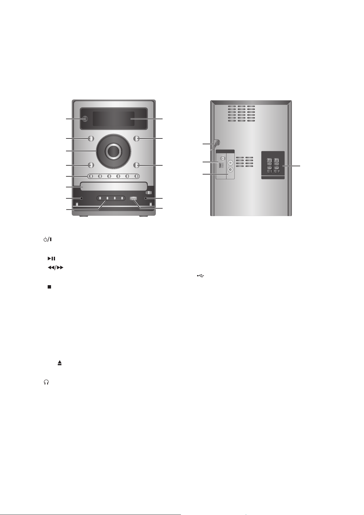
LOCATION OF USERS CONTROLS
17
15
16
14
1
2 12
11
10
13
4
5
6
7
8 9
3
1. (POWER)
2. CD
3. • (PLAY/PAUSE)
• (SKIP/SEARCH)
TUNE.-/+
• (STOP)
• VOLUME CONTROL KNOB
4. USB
5. • XDSS plus
• XTS pro
• EQ Master
• ST./MONO
• PROG.
• CD
6. DISC TRAY
7. (Headphone jack) : ø3.5mm
8. • DEMO
• TIMER
• CLOCK
• SET (RDS - OPTIONAL)
9. (USB connector)
10.PORT.IN jack
11.AUX (PORTABLE)
12.TUNER
13.DISPLAY WINDOW
14.POWER IN (POWER CORD)
15.AM/FM ANTENNA TERMINAL
16.AUX IN (AUXILIARY INPUT) connector
17.SPEAKER TERMINAL
FRONT / BACK PANEL
1-5
Page 7
1-6
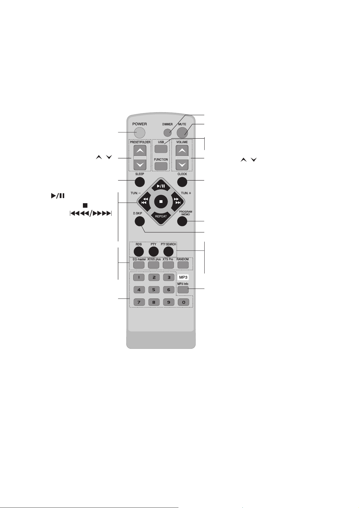
REMOTE CONTROL
POWER
PRESET/FOLDER(
)
SLEEP
•
(PLAY/PAUSE) •
(STOP) •
(SKIP/SEARCH)
TUN.-/+ •
REPEAT •
EQ master •
XDSS plus •
XTS Pro •
RANDOM •
NUMERIC
/
DIMMER
MUTE
• USB
• FUNCTION
VOLUME ( )
CLOCK
PROGRAM/MEMO
D.SKIP
RDS (Radio Data System) FUNCTION
• RDS : OPTIONAL
• PTY : OPTIONAL
• PTY SEARCH : OPTIONAL
MP3 Info
(MP3/WMA
file information display)
/
Page 8

SPECIFICATIONS
• GENERAL
Power supply Refer to the back panel of the unit.
Power consumption Refer to the back panel of the unit.
Net Weight 3.0kg
External dimensions (WxHxD) 174 x 245 x 278mm
• TUNER
FM Tuning Range 87.5 ~ 108.0MHz or 65 ~ 74MHz, 87.5 ~ 108.0MHz
Intermediate Frequency 10.7MHz
Signal to Noise Ratio 60/55dB
Frequency Response 50 ~ 10000Hz
AM Tuning Range 522 ~ 1620kHz or 520 ~ 1720kHz
Intermediate Frequency 450kHz
Signal to Noise Ratio 30dB
Frequency Response 140 ~ 1800Hz
• AMPLIFIER
Output Power 50W + 50W
T.H.D 0.5%
Frequency Response 40 ~ 20000Hz
Signal-to-noise ratio 75dB
• CD
Frequency response 40 ~ 20000Hz
Signal-to-noise ratio 75dB
Dynamic range 75dB
• SPEAKERS
Type 2 Way 2 Speaker
Impedance 4
Frequency Response 80 ~ 20000 Hz
Sound Pressure Level 82dB/W (1m)
Rated Input Power 50W
Max. Input Power 100W
Net Dimensions (WxHxD) 160 x 243 x 174mm
Net Weight (1EA) 2.02kg
1-7
Page 9

MEMO
1-8
Page 10
A
C
D
H
I
D
F
H
I
A
B
K
E
J
F
L
G
B
C
E
G
J
K
L
256
250
254
252
454
A26
A52
454
A46
305
454
454
454
A47
263
266
264
290
454
454
454
259
CAB LE 3
CAB LE 2
A43
255
257
267
256
258
SMPS
CD
MAIN
FRO NT
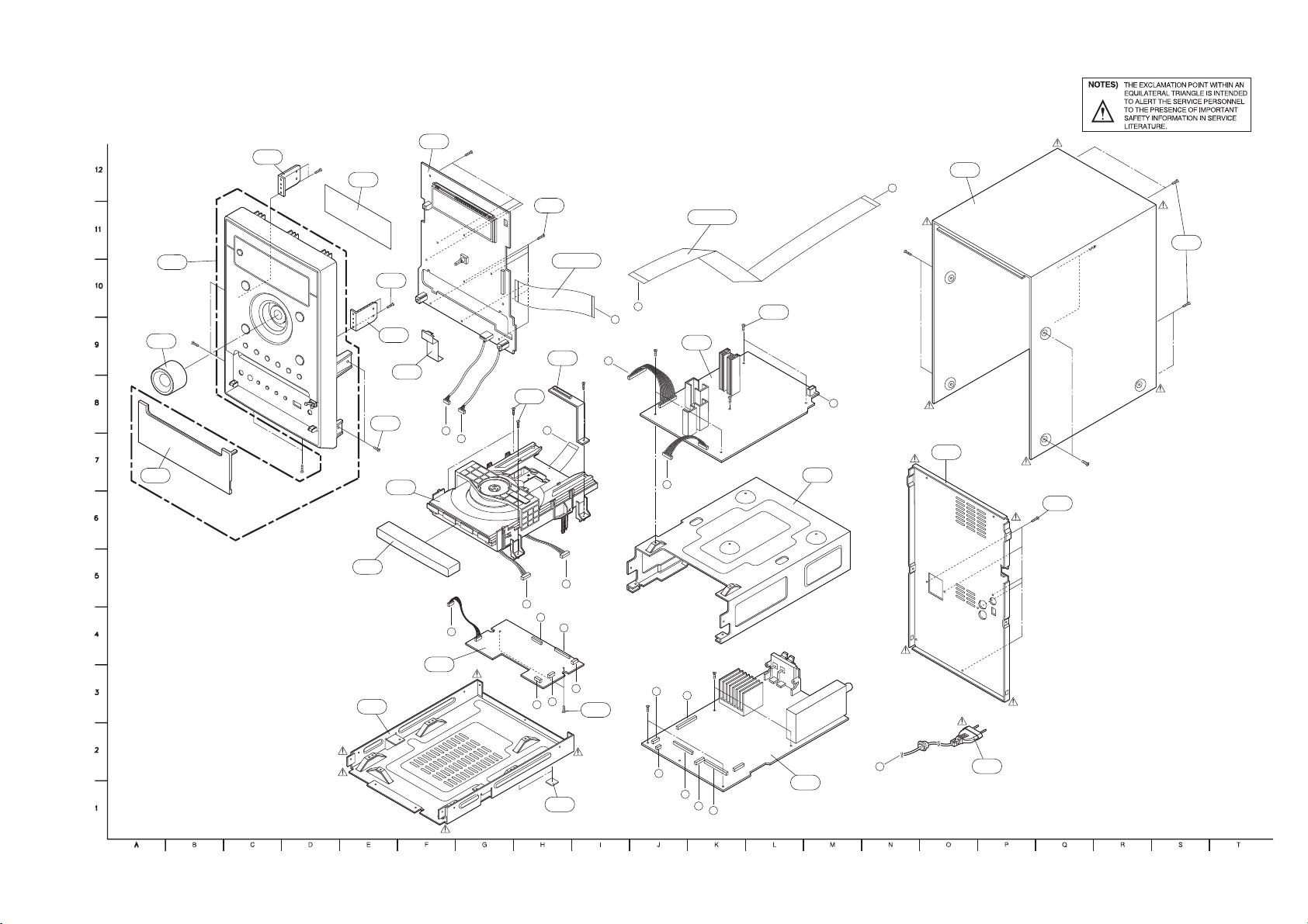
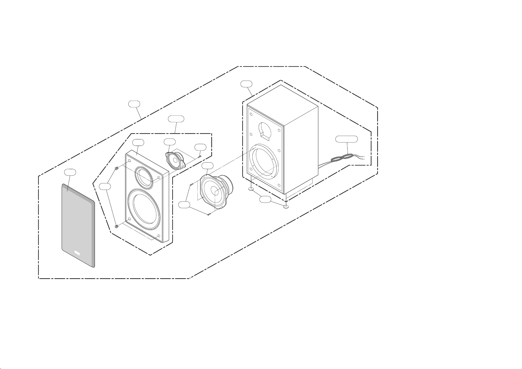
SECTION 2 EXPLODED VIEWS
CABINET EXPLODED VIEW
Page 11
A26
018
A02
020
A01
001
002
003
010
432
432
431
026
037
012
012
019
A03
016
015
036
012A
012A
439
014
013
017
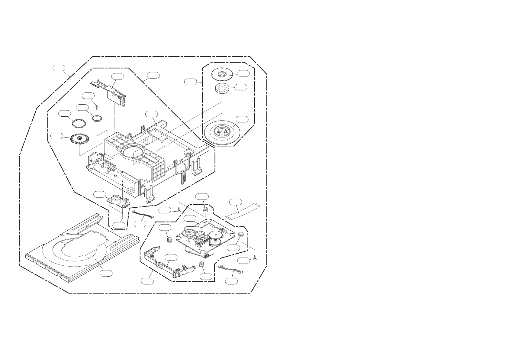
CD MECHANISM (CDM-330) EXPLODED VIEW
Page 12
850
851
852
853
854
855
856
857
858
WIRE80
A80
A80A
SPEAKER EXPLODED VIEW
MODEL : XCS102F
Page 13

MEMO MEMO
2-7 2-8
Page 14
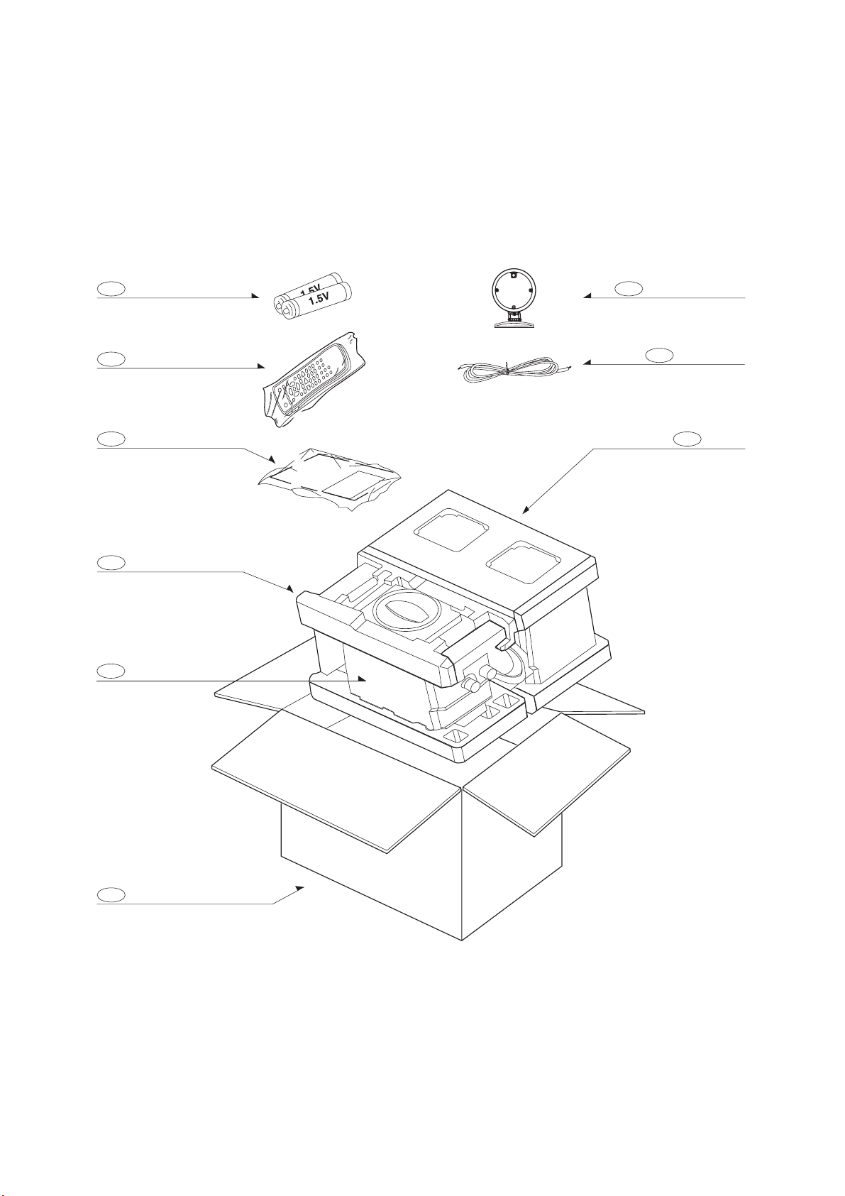
2-9
PACKING ACCESSORY VIEW
808 Battery
900 Remote Control
801 Instruction Ass'y
803 Packing
803 Packing
804 Bag
802 Box
825 Antenna (FM)
824 Antenna Loop (AM)
Page 15
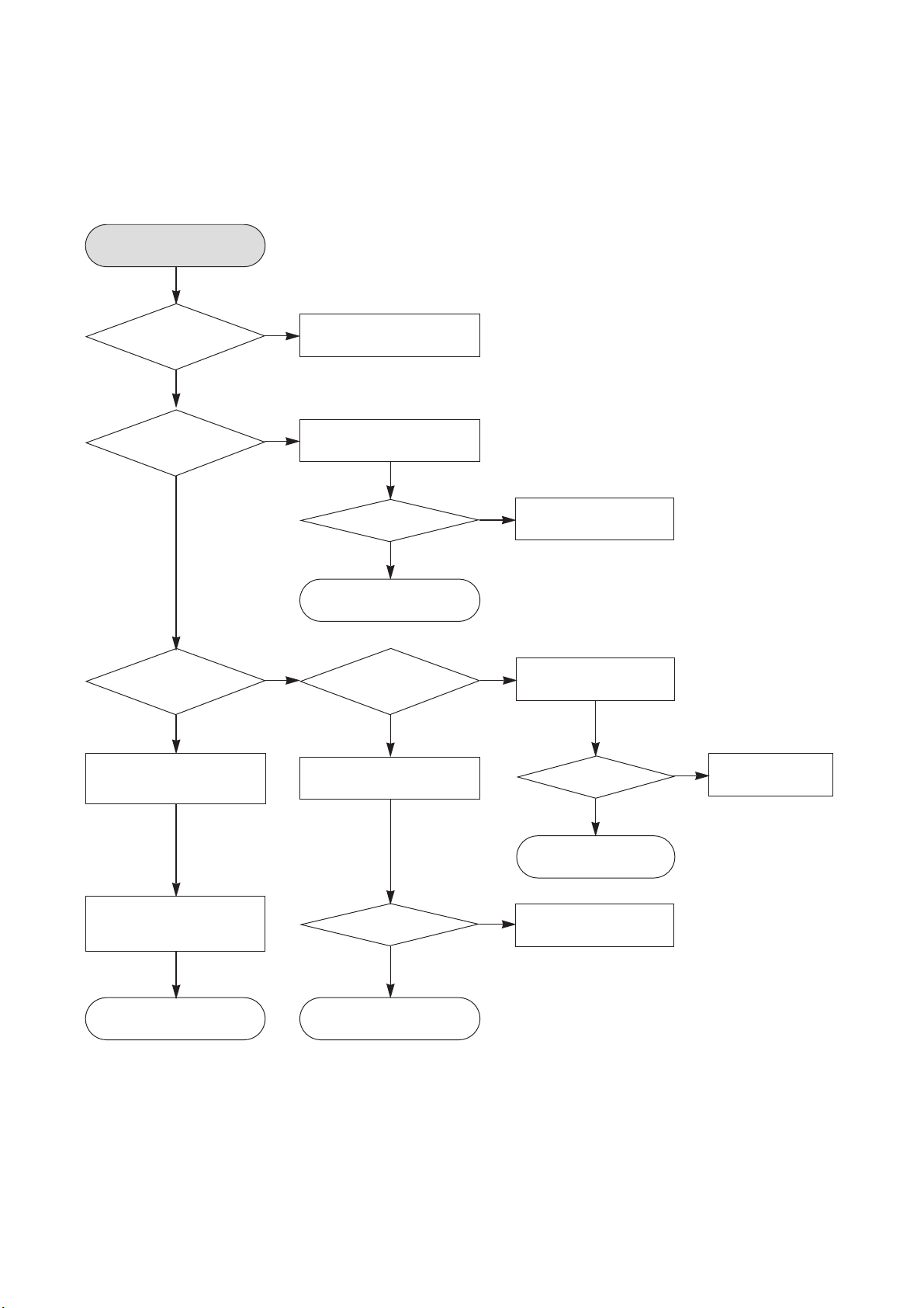
3-1
AUDIO ELECTRICAL TROUBLESHOOTING GUIDE
SECTION 3 AUDIO PART ELECTRICAL
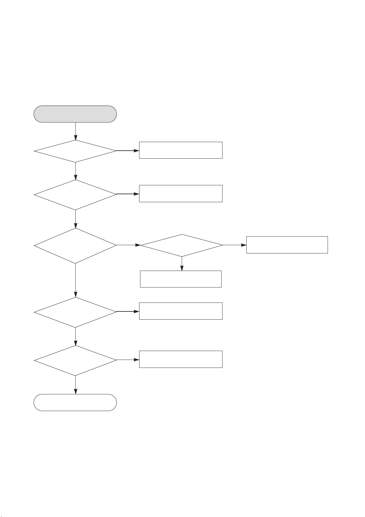
1. POWER (SMPS)
POWER (SMPS)
OK
YES
YES
YES
Replace IC 901,902
Check IC901, 902
Check the fuse
F901
NONO
NO
YES
Check short of
P9701, P9702 line
Replace the fuse
Check
the DC V of C905.
If DC V is over
400V
NO
Check BD901, LF901, 902
Check the
DC V of C981, C945.
If DC V is 6.1V
NO
Check short of P9702 line
YES
YES
Chcek the
DC V of C950, C951
If DC V is in
31.5V
NO
Check short of P9701 line
Chcek the
DC V of C909, C903,
C921 If DC V is in 14~19V
and it is steady.
YES
Page 16
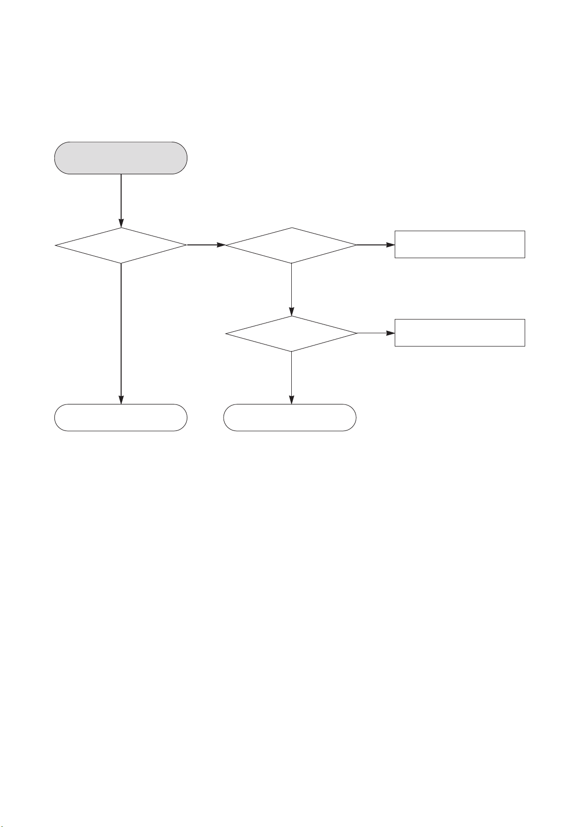
2. P-SENS
P-SENS
YES
Check
the PIN6 of P9702
If DC V is over 5.6V
3. VKK CHECK
VKK check
Check
the PIN3 of P9702
If DC V is over -28V ±2
OK
OK
YES
YES
YES
NO
NO
Check power circuit Trouble shooting
Check power circuit Trouble shooting
4. MICOM PART CHECK I
MICOM part check I
YES
Check P-SENS
(P7904)_PIN6.
YES
Check both
end voltage of IC101
(KIA7042).
YES
Check voltage of IC100
78KO/KF2_PIN1.
YES
OK OK
NO
SMPS troubleshooting.
NO
Check if IC101(KIA7042) of
output voltage is over 4.3V.
Refer to
Check
if input voltage of
IC101(KIA7042) is
over 5V.
YES
YES
3-2
NO
Check the
periphery of IC101
(KIA7042).
YES
NO
Replace IC101
(KIA7042).
Page 17
5. MICOM PART CHECK II
MICOM part check II
YES
Check if
voltage of P7904_PIN5
is 5.6V.
YES
Check
both end voltage of
D101
YES
Check
Q101_ emitter/collector
5V.
YES
Check if IC103_PIN8 and
IC100_PIN19, 20, 59 are 5V.
NO
NO
NO NO
Q102_collector 0.6V LOW.
Refer to
SMPS troubleshooting.
Check if output of
D101(RL104) is 5V.
YES
Check D101.
YES
OK
Check Q102_base
0.6V HIGH.
YES
NO
Replace D101.
Check if output of IC101
(KIA7042) is over 4.3V.
YES
Check IC101.
NO
Replace IC101.
YES
X101 : 32.768kHz
X100 : 9.8304MHz
Check the operation.
YES
OK
YES
Check Q102.
YES
OK
3-3
NO
YES
OK
Replace Q102.
Page 18
3-4
Check
IC100(78KOKF2)_
PIN 22, 24
OK
YES
YES
Refer to
micom troubleshooting
Check micom
voltage 5V.
PIN22
DATA PIN24 CLK
NONO
YES
Replace micom.
Check micom.
NO
YES
OK
6. IC103(KS4CD21CS) CHECK
Page 19

3-5
FLD display check
YES
YES
Replace WF31.
Check each
PIN voltage.
NO
NO
YES
YES
OK
Replace IC301.
Check IC301.
NO
YES
Replace IC100FLD light on?
Check IC100.
NO
YES
YES
OK
Refer to SMPS
7. FLD DISPLAY CHECK
YES
YES
Check
P7904_PIN1, 2, 3 voltage
input.
NO
Check WF31 connection.
NO
If voltage is not 5V,
check input and output
of D301(1SR35).
YES
Check WF31
connection and power.
Pin1 : FL-22 Pin2 : FL+26
Pin3 : VKK- over
26V.
YES
YES
YES
YES
OKOK
76 PIN - > DO - - >
Check DATA in Check IC100.
NO
IC100
75 PIN - > STB
77 PIN - > 4PIN DI
78 PIN - > 1PIN CLK
Check data output.
IC100 - >
Check IC301
DATA communication.
PIN PIN
75PIN - > 3PIN STB
76PIN - > 2PIN D
78PIN - > 1PIN
CLK
Check
IC301(PT6324) voltage.
Pin50 VKK : -26V
PIN9.52 : +5V
Check if both end votage
of F1, F2 are over 3.7V.
VKK : over 26V.
Page 20

8. PWM MODULATION PART CHECK
PWM modulation
part check
YES
P7905_PIN9
3.3V checking
NO
Refer to
SMPS troubleshooting.
YES
Check IC604(PS9829)
VDD PIN voltage(3, 7, 8,
10, 22, 29, 39, 47, 56, 65,
72, 94).
Check X601_PIN2 3.3V.
YES
Check
X601 12.288MHz
operation.
YES
Check IC605_
PIN3 input and PIN2
output.
YES
IC604
(PS9829) PIN86 CLK
input check
YES
Check
IC100(78KOKF2)
21->PWM_CLK
22->PWM_DATA
43->PWM_REST
output.
YES
NO
NO
NO
NO
Check X601
12.288MHz.
Check IC605_
Check IC605_
Check IC605_
PIN2 output
Check R680
(470) output.
LINE registor output.
DATA:R671, CLK:R670
YES
OK
PIN8 3.3V.
YES
PIN3 input
YES
YES
OK
YES
OK
Check
RST:R665
YES
OK
NO
NO
NO
NO
NO
NO
Replace X601.
Check FB614
BEAD input, output and
voltage.
YES
OK
Check X601
2.288MHz
YES
Replace IC605.
Replace R680.
Replace R670, R671
and R665
NO
NO
Replace FB614
Replace X601.
OK
Check IC604
(PS9829) DATA input.
78 PIN->DATA
79 PIN->CLK
YES
Check PWM
modulator output.
FL:75(+)74(-)
FR:71(+)70(-)
YES
NO
NO
Check
DVD ASS`Y(PS9829)
communication
(P7403).
YES
Check
IC604(PS9829) DATA
input.
YES
OK
Check IC604(PS9829).OK
3-6
NO
NO
Refer to
CD troubleshooting.
Check each LINE
registor output.
Page 21

3-7
Power AMP part check
YES
Check each LINE registor output voltage.
IC700 : R701, 702, 726, 727
NO
Check
IC700 PIN1,17, 18, 19, 36
+12V input.
Refer to SMPS troubleshooting.
YES
YES
YES
NO
P7905_3PIN : +12V,
PIN13, 14, 15 : 35V.
YES
Replace the coils
YES
NO
Check output line coil.
Check PWM modulator input.
Each IC PIN4, 6, 14, 16
YES
Power IC700 PIN20, 27, 29, 34 output.
Check IC700 PIN21, 26, 29, 34 input voltage.
OK
9. POWER AMP PART CHECK
Page 22

10. AUX FUNCTION CHECK
AUX function check
YES
Check JK800 connection.
YES
Check
IC200(BU4052)_
PIN4, 11 input
waveform.
YES
Check IC200(BU4052)_
PIN3, 13 output waveform.
YES
Check
IC801(MC4580)_PIN 2, 6
input waveform.
YES
NO
NO
IC200(BU4052)_PIN16
Check
VDD, PIN8 VSS
power.
YES
Replace IC200
Check
IC801(MC4580)_PIN4
VSS, PIN8 VDD
power.
YES
Replace IC801OK
NO
NO
Check µ-COM(IC301)_
PIN83, 84 commucation.
Refer to
SMPS troubleshooting.
3-8
Page 23

11. TUNER FUNCTION CHECK
TUNER function check
YES
Check TUNER
module(TU601) operation.
YES
Check IC200(BU4052)_PIN1, 12 input
waveform.
YES
Check
IC200(BU4052)_PIN3, 13
output waveform and IC601
(BU4052)_PIN2,15 input
waveform.
YES
Check IC801(MC4580)_
PIN2, 6 input waveform.
NO
NO
NO
Check TUNER module voltage(PIN2 : 9V).
Check IC200(BU4052)_
PIN16 VDD, PIN8 VSS power.
YES
Replace IC200.
Replace IC200.
Check IC801(MC4580)_
PIN4 VSS, PIN8 VDD power.
YES
OK
YES
Replace IC801.
3-9
Page 24

12. PORTABLE IN FUNCTION CHECK
PORTABLE IN function check
YES
Check JK32 connection.
YES
Check
IC200(BU4052)_
PIN5, 14 input
waveform.
YES
Check IC200(BU4052)_
PIN3, 13 output waveform.
YES
Check
IC801(MC4580)_PIN 2, 6
input waveform.
YES
NO
NO
IC200(BU4052)_PIN16
Check
VDD, PIN8 VSS
power.
YES
Replace IC200
Check
IC801(MC4580)_PIN4
VSS, PIN8 VDD
power.
YES
Replace IC801OK
NO
NO
Check µ-COM(IC301)_
PIN83, 84 commucation.
Refer to
SMPS troubleshooting.
3-10
Page 25

INTERNAL BLOCK DIAGRAM OF ICs
1. AK5358
VA AGND VD DGND MCLK
Clock Divider
AINL
AINR
VCOM
2. BU4052
Modulator
Modulator
Voltage Reference
Decimation
Filter
Decimation
Filter
Serial I/O
Interface
DIFPDNCKS0CKS1CKS2
LRCK
SCLK
SDTO
3-11
Page 26

3. LC78692NW
SLCO
80
LRVSS
RCHO
LRREF
LCHO
LRVDD
XVDD
XIN
XOUT
XVSS
AMUTEB
DOUT
DVDD
DVSS
DVDD15
VVSS2
VPDOUT2
VCOC2
VPREF
VVDD2
79
78
77
76
75
74
73
72
71
70
69
68
67
66
65
64
63
62
61
EFMIN
RFOUT
LPF
PHLPF
AIN
CIN
BIN
DIN
SLCISET
RFMON
VREFO
JITTC
EIN
FIN
PCNCNT
TEOUT
TEIN
LDD
LDS
AVSS
1
2
3
4
5
6
7
8
9
10
11
12
13
14
15
16
17
18
19
20
SLICE
LEVEL
CONTROL
RF
SIGNAL
PROCESSOR
MONITOR
VREF
TES, HFL,
DEFECT
JITIER
APC
D/A
A/D
LPF
1 Bit
DAC
GENERATOR
8FS DIGITAL
DEEMPHASIS
ATTENUATION CONTROL
Bass-Boost
INTERPOLATION MUTE
ERROR CORRECTION
Synchronization
Detection
Demodulation
CONTROL
CD PLL
CLOCK
FILTER
EFM
SERVO
DOUT
Control
DECODER
DECODER
SUBCODE
DECODER
MP3
&
WMA
ROM
TEXT
PORT
CONTROL
Audio Output
Memory I/F
PLL2
Control
Stream
Control
Memory
1M Bit
System
Control
MCU
PLL3
I/F
60
59
58
57
56
55
54
53
52
51
50
49
48
47
46
45
44
43
42
41
LRSY
DATACK
DATA
TEST1
STDATA
STCK
STREQ
TEST0
CONT0
CONT1
CONT2
INTB1
INTB0
RESB
DO
DI
CL
CE
DVSS
DVDD
21
22
23
24
25
26
27
28
29
30
31
32
33
34
35
36
37
38
39
40
FDO
AVDD
TDO
SPDO
SLDO
VVSS1
PDOUT1
PDOUT0
VVDD1
PCKIST
PUIN
DMUTEB
DEFECT
C2F
FSEQ
DVSS
DVDD
DVDD15
VVSS3
VVDD3
3-12
Page 27

4. PS9829B
MBCK
SBCK
SLRCK
MLRCK
MSDIN[0:3]
SSDIN[0:3]
MIC_MCLK
DMIX_MCLK
OLRCK
OBCK
DMIX_SDOUT
PWM1_P/M
PWM2_P/M
PWM3_P/M
PWM4_P/M
PWM5_P/M
PWM6_P/M
PWM7_P/M
PWM8_P/M
PWM_HP_L_P/M
PWM_HP_R_P/M
PWM_SWL_P/M
EPD_ENA
OVERLOAD
MIC_BCK
MIC_LRCK
MIC_SDIN
SPI/I2C
SO/SDA
SCK/SCL
SI/I2C_AD0
/
CS/I2C_AD2
EXT_MUTE
CLK_IN
/RESET
PLL_DVDD
PLL_DVSS
PLL_AVDD
PLL_AVSS
DVDD
DVSS
IO_VSS
IO_VDD
Internal Controls
Internal Clock Internal Reset
Host
Interface
(I
2
C, SPI)
Mic,
Input
Processor
Input
Mapper
Sample
Rate
Converter
Input
&
Output
MUX
Serial Audio
Output
Interface
Down
Mixer
Mixer
4 Band
EQ
Bass
Manager
Main
Volume
Trim
Volume
Serial
Audio
Output
Interface
PWM
Modulator
POP
NR
Power Supply
Output Mapper
PLL
Reset & Power Down
Automatic
Gain
Limiter
5. PT6324
SG1/KS1
SG2/KS2
SG3/KS3
SG4/KS4
SG5/KS5
SG6/KS6
SG7/KS7
SG7/KS7
SG8/KS8
SG9/KS9
SG10/KS10
SG11/KS11
SG12/KS12
SG13/KS13
SG14/KS14
SG15KS15
SG16/KS16
SG17
SG18
SG19
SG20
SG21
SG22
SG23
SG24
GR1
GR2
GR3
GR4
GR5
GR6
GR7
GR8
GR9
GR10
GR11
GR12
GR13
GR14
GR15
GR16
Segment Driver
Dimming Circuit
Grid
Driver
Control
DIN/DOUT
CLK
STB
OSC
LED1
K1 K2 VDD GND VEE
Timing Generator
Key Matrix Memory
LED
Driver
CSC
Serial
Data
Interface
Display Memory
3-13
Page 28

6. STR-W6753
4
Vcc
Start
Stop
Burst
OSC
Protection
latch
DRIVE
Reg
Delay
Burst
Control
BSD
OCP
GND
S
D
FB
FB
OCP/BD
SS/OLP
BD
Q
Q
S
S
R
R
MaxON
R Q
S
OLP
Reg&
Iconst
Soft Start
Counter
Bottom Selector
5
7
6
3
2
1
OVP
3-14
Page 29

7. TAS5142
2nd-Order L-C
Output Filter
for Each
Half-Bridge
Bootstrap
Capacitors
2-Channel
H-Bridge
BTL Mode
System
Microcontroller
OUT_A
OUT_B
OUT_C
OUT_D
BST_A
BST_B
BST_C
BST_D
RESET_AB
RESET_CD
System
Power
Supply
Hardwire
Mode
Control
PVDD
GVDD (12 V)/VDD (12 V)
GND
Hardwire
OC Limit
M1
M3
PVDD
Power
Supply
Decoupling
32 V
12 V
GND
VAC
PWM_A
PWM_C
PWM_D
PWM_B
V
ALID
M2
Left-
Channel
Output
Right-
Channel
Output
Input
HúBridge 1
Input
H-Bridge 2
GVDD
VDD
VREG
Power Supply
Decoupling
4
PVDD_A, B, C, D
GND_A, B, C, D
GVDD_A, B, C, D
4 4
VDD
GND
VREG
AGND
OC_ADJ
Bootstrap
Capacitors
2nd-Order L-C
Output Filter
for Each
Half-Bridge
SD
OTW
Output
H-Bridge 2
Output
H-Bridge 1
OTW
SD
T
AS5508
3-15
Page 30

8. U1739EJ2V1UD00/KF2_E
Port 0 P00 to P067
Port 1 P10 to P178
Port 2 P20 to P27
7
Port 3 P30 to P33
4
Port 4 P40 to P47
8
Port 5 P50 to P57
8
Port 6 P60 to P67
8
Port 7 P70 to P77
8
Port 12 P120 to P124
5
Port 13
P130
Port 14 P140 to P145
6
8
4
2
Key return
Reset control
On-chip debug
Note 2
Multiplier &
divider
System
control
Voltage
regulator
REGC
XT2/EXCLKS/P124
XT1/P123
XT1/P121
RESET
OCD0A
Note 2
/X1, OCD1A
Note 2
/P31
KR0/P70 to
KR7/P77
OCD0B
Note 2
/X2, OCD1B
Note 2
/P32
X2/EXCLK/P122
Internal high-speed
oscillator
8
Buzzer output
BUZ/P141
Clock output
control
Power on clear/
low voltage
indicator
POC/LVI
control
PCL/P140
EXLVI/P120
VDD,
EVDD
VSS,
EVSS
FLMD0
16-bit timer/
event counter 00
TO00/TI010/P01
TO01/TI011/P06
TI000/P00
TI001/P05
TOH0/P15
TOH1/P16
TI50/TO50/P17
TI51/TO51/P33
RxD0/P11
TxD0/P10
RxD6/P14
TxD6/P13
SI10/P11
SO10/P12
SI11/P03
SO11/P02
SCK11/P04
SCK11/P05
SIA0/P143
SOA0/P144
SCKA0/P142
STB0/P145
BUSY0/P141
EXSCL0/P62
SDA0/P61
SCL0/P60
AV
REF
RxD6/P14 (LINSEL)
INTP0/P120
INTP1/P30 to
INTP4/P33
INTP5/P16
INTP6/P140,
INTP7/P141
AV
SS
ANI0/P20 to
ANI7/P27
SCK10/P10
RxD6/P14 (LINSEL)
16-bit timer/
event counter 01
8-bit timer H0
8-bit timer H1
Watchdog timer
78K/0
CPU
core
Internal
high-speed
RAM
Internal
expansion
RAM
Flash
memory
BANK
Note 1
Watch timer
8-bit timer
event counter 50
8-bit timer
event counter 51
Serial
interface UART0
LINSEL
Serial
interface UART6
Serial
interface CSI10
Serial
interface CSI11
Serial
interface CSIA0
Serial
interface IIC0
A/D converter
Interrupt
control
Internal low-speed
oscillator
3-16
Page 31

9. UTC MC4580
9-2. TEST CIRCUIT
9-1. PIN CONFIGURATION
3-17
Page 32

3-18
6
P
5
P
16
P
8P
D PCB
2 CH SPK
AU
X
JACK
TUNER
MODUL
E
1
CD
INGLE M
D
P
CB
5
P
3
P
29
P
USB
PORT
IN
H/P
FRONT PCB
SMPS PCB
15
P
[Total CNT Q'ty : 10ea]
1. SMPS MAIN : 2ea
2. MAIN CD : 2ea
3. MAIN FRONT : 1ea
4. FRONT CD : 1ea
5. CD MD : 3ea
E
D
3-19
WIRING DIAGRAM
Page 33

AC INPUT
ZNR &
FILTER
T
R
A
N
S
#1
AMP
Switch
IC #
1
MAIN
Switch
IC #
2
T
R
A
N
S
#2
FL1-FL2 (4. 5V)
-12V
12V (78R12)
5V(P-SEN S)
6.1V (KIA278R05)
P9702
P9701
FEED BACK
AMP (+) 31.5V
3.5V (278R35)
-31. 5V(VKK)
RECTIFICATION
SMOOTHING
CIRCUIT
FEED BACK
3-20 3-21
BLOCK DIAGRAMS
1. SMPS BLOCK DIAGRAM
Page 34

PS9829B
PWM
MODULATOR
PS9829B
PWM
MODULATOR
TAS5142
Power Amp
TAS5142
Power Amp
FR
FL
FL+/ -, FR+/-
AMP BOARDMAIN BOARD
NEC
AUDIO
MICOM
NEC
AUDIO
MICOM
12.288 MHz
9.8304 MHz
9829_RESET
9829_CLK
9829_DAT
TAS5142_PDN
TAS5142_SD
HA1227
TAPE IC
REC MUTE
P/B MUTE
REC BIAS
DECK
MD
DECK/ HD
TUNER
MODULE
PLL DAT.CLK
RDS
DATA.CLK
BU4052
TAPE L/R
TUNER L/R
AUX L/R
OP AMP
AK5358
OP AMP
LEVEL METER
REC L/R
AK5358 REST
CD DATA.CLK
PORT INPUT
AUX INPUT
HEAD PHONES
BU4052 DATA
USB DA+.-. 5V
CD DATA.CLK
AK5358
CLK.DATA
H/P_SW
PW
M OUT
CD
SANYO
LC78692NW
FLD (DISPLAY)
VFD DRIVE IC
PT6324
XC102 : 2 CH (50W X 2Ch)
W/O DECK
XC62 : 2 CH (30W X 2Ch )
W /SINGLE DECK
LEVEL SHIFT IC
74VHCT244
R
L
PORT L/R
SOL "B"
MOTOR
MODE B
HALF B
P/B
L/R
REC L/R
XC62 ONLY
3-22 3-23
2. MAIN & FRONT BLOCK DIAGRAM
Page 35

SCHEMATIC DIAGRAMS
1. SMPS SCHEMATIC DIAGRAM
WHEN SERVICING TH IS CHASSI S, UNDER NO
CIRCUMSTANCES SHOULD THE ORIGINAL DESIGN
BE MODIFIED OR ALTERED WITHOUT PERMISSION
FROM THE LG CORPORATION. ALL COMPONENTS
SHOULD BE REPLACED ONLY WI TH TYPE S
IDENTICAL TO THOSE IN THE ORIGINAL CIRCUIT.
SPECIAL COMPONENTS AR E SHADE D ON THE
SCHEMATIC FOR EASY IDE NTIFICATION. THIS
CIRCUIT DIA GRAM MAY OCCASION ALLY DIFFER
FROM THE ACTUAL CIRCUIT US ED. THIS WAY,
IMPLEMENTATION OF THE LATEST SAFETY AND
PERFORMAN CE IMPROV EMENT CHANGE S INTO
THE SET IS NOT DELAYED UNTIL THE NEW SERVICE
LITERATURE IS PRINTED.
1. Shaded( ) parts are critical for safety. Replace only
with specified part number.
2. Voltages are DC-measured with a digital voltmeter
during Play mode.
IMPORTANT SAFETY NOTE :
3-24 3-25
Page 36

3-26 3-27
2. MAIN SCHEMATIC DIAGRAM
Page 37

3. AMP SCHEMATIC DIAGRAM
3-28 3-29
Page 38

3-30 3-31
4. FRONT SCHEMATIC DIAGRAM
Page 39

1. MAIN P.C.BOARD
(TOP VIEW)
PRINTED CIRCUIT BOARD DIAGRAMS
3-32 3-33
Page 40

MAIN P.C.BOARD
(BOTTOM VIEW)
3-34 3-35
Page 41

2. SMPS P.C.BOARD
3-36 3-37
Page 42

3. FRONT P.C.BOARD
(TOP VIEW) (BOTTOM VIEW)
3-38 3-39
Page 43

MEMO MEMO
3-40 3-41
Page 44

4-1
CD ELECTRICAL TROUBLESHOOTING GUIDE
1. CD PART TROUBLESHOOTING
Turn on CD
YES
YES
NO
OPEN CLOSE check
Connector check (PN804)
NO
Check voltage CN806
PIN1 : 12, PIN2 : 6.3V
NO
Check voltage PN805
PIN22 : CLOSE, PIN23 : OPEN
YES
NO
“Reading”
Display check
Connector check
(PN802, PN803, PN804, CN806)
NO
Check micom interface circuit (PN805)
(CE, BTL-MUTE, CD-IN, CD-OUT, CLK, WRQ, FSEQ)
YES
NO
Reading OK check
Connector check (PN801,PN802)
NO
YES
If PALY, AUDIO
OUTPUT check
Check PN805 audio data
PIN10 : DA_LRCK (IC801 PIN60 LRSY)
PIN11 : DA_BCK (IC801 PIN59 DATACLK)
PIN12 : DA_DATA0 (IC801 PIN58 DATA)
NO
Check pick up movement
NO
Check AM5810FP (IC802)
NO
Check LC78692 (IC801)
OK
SECTION 4 CD PART ELECTRICAL
Page 45

4-2
1-1. OPEN CLOSE NG
Connector locking check (PN804)
YES
YES
YES
YES
Check power
supply circuit (PN805, CN806)
CN806 PIN1 : 12V, PIN2 : 6.3V
PN805 PIN8 : +5V_AD
Defective main power supply
NO
Check voltage change LO+, LO- OF IC803
(PN805 PIN23 : OPEN, PIN22 : CLOSE)
Defective IC803
Defective mechanism
NO
Check voltage
change of OPEN CLOSE
IC803 INPUT voltage PIN6 : 12V,
PIN7:6.3V (PN805 PIN2 :
BTL_MUTE, 23 : OPEN,
22 : CLOSE)
Defective micom
NO
Page 46

1-2. “READING” DISPLAY CHECK (= ONLY “CD” DISPLAY)
Conector locking check
(PN802, PN804, PN805, CN806)
YES
Check power
supply port (PN805, CN806)
CN806 PIN1 : 12V, PIN2 : 6.3V,
PIN4 : 5V PN805
PIN8 = 5V_AD
YES
NO
Defective connector or main power supply
Check voltage
The PIN2 of IC804
IC804 PIN2 : 3.3V
YES
Check reset
signal of PN805
PN805 PIN19 : 5V
YES
Check micom interface circuit (PN805)
PN805 PIN1, 3, 4, 15, 19, 26 signal check
(1 : CE, 3 : DI, 4 : CLK, 15 : D0, 19 : RST,
18 : FSEQ, 26 : WRQ) PIN3 DI : From DSP
to micom PIN15 DO : From micom to DSP
Check the waveform #1
YES
NO
NO
NO
Defective IC804
Defective micom or connector
Defective micom or connector
Defective IC801
4-3
Page 47

4-4
Connector locking check
(PN801, PN802)
Is reading OK?
Defective pick up or
IC802 or IC801
Does sled move?
NO
NO
Check PN802
PIN3, 4 (SL+, SL-)
1-3. READING OK CHECK (= “NO DISC” DISPLAY)
Does lense move?
(= UP & DOWN)
YES
A
YES
Defective pick up or
IC802 or IC801
NO
NO
Check PN801
PIN13, 16 (FA+, FA-)
B
Defective pick up or IC801
Does laser light?
NO
NO
Check PN801 PIN10 (LD)
YES
C
Defective pick up or
IC802 or IC801
Does spindle rotate?
NO
NO
Check PN802
PIN5, 6 (SP+, SP-)
YES
D
Defective pick up or
IC802 or IC801
NO
NO
Check PN801
PIN14, 15 (TA+, TA-)
E
Page 48

1-4. READING OK CHECK #A (= “NO DISC” DISPLAY)
A
Does
SL+ waveform
appear at (IC802 PIN13
and PN802 PIN3)
waveform #2
sled motor
wave
YES
Check PN802 connector line
YES
NO
NO
Defective PN802 connector
Defective pick up sled motor
Does slin
waveform appear at
(IC802 PIN5)
waveform #2
sled drive
wave
YES
Defective IC802
1-5. READING OK CHECK #B (= “NO DISC” DISPLAY)
B
NO
Defective IC801
Does
FA+ waveform
appear at (IC802 PIN16
and PN801 PIN13)
waveform #3 focus
coil drive
wave
YES
Check PN801 connector line
YES
NO
NO
Does
fain-waveform
appear at (IC802 PIN25)
waveform #3
focus drive
wave
YES
Defective IC802
Defective PN801 connector
Defective pick up
focus actuator
4-5
NO
Defective IC801
Page 49

4-6
Defective IC804
Is ?V applied
to PIN10 of PN801
laser supply voltage
check
Is 3.3V
applied to
PIN30, 36, 39, 41, 61,
68, 75 of IC801 RF IC
supply voltage
check
NO
NO
1-6. READING OK CHECK #C (= “NO DISC” DISPLAY)
YES
YES
Defective IC801
Is 2.3V
PIN18 (LDO) of IC801
laser control voltage
check
NO
YES
C
Defective Q801 or D801
NO
Defective PN801 connector
Defective pick up laser part
Check PN801 connector line
YES
Page 50

1-7. READING OK CHECK #D (= “NO DISC” DISPLAY)
D
Does
SP+ waveform
appear at (IC802
PIN11 and PN802 PIN5)
waveform #4 spindle
motor drive
wave
YES
Check PN802 connector line
YES
NO
NO
Does
spin waveform
appear at (IC802 PIN6)
waveform #4
spindle drive
wave
YES
Defective IC802
Defective PN802 connector
Defective pick up
spindle motor
NO
Defective IC801
4-7
Page 51

1-8. READING OK CHECK #E (= “NO DISC” DISPLAY)
E
Does
TA+ waveform
appear at (IC802 PIN17
and PN801 PIN14)
waveform #5 tracking
coil drive
wave
YES
Check PN802
connector line
YES
Does
ARF signal appear?
(IC801 PIN 2)
waveform #6
YES
NO
NO
NO
Does
tain - waveform
appear at (IC802 PIN22)
waveform #5
tracking drive
wave
YES
Defective IC802
Defective PN802 connector
Defective pick up or IC801
NO
Defective IC801
Does FE, TE signal
appear? (IC801
PIN10 : RFMON, PIN16 : TE)
waveform #6
* REMON is FE
NO
Defective pick up or IC801
4-8
Page 52

2. USB PART TROUBLESHOOTING
Turn on USB
YES
“Checking” or
“USB” display check
YES
Reading OK check
YES
If PLAY, AUDIO
OUTPUT check
YES
NO
NO
NO
Connector check
(PN805, CN806, PN810 )
NO
Check power supply circuit (CN806)
NO
Check micom interface circuit (PN805)
PIN13 : RX (IC805 PIN49 : TXD)
PIN14 : TX (IC805 PIN33 : RXD)
Check PN810 1PIN : 5V
NO
Check PN810 PIN2(D-), 3(D+)
NO
Check OTI6888 (IC805)
Check signal STCK, STREQ, STDATA
STCK : IC805 PIN52, IC801 PIN55
STREQ : IC805 PIN53, IC801 PIN54
STDATA : IC805 PIN54, IC801 PIN56
NO
4-9
Connector check (CN806)OK
Page 53

WAVEFORMS OF MAJOR CHECK POINT
PIN26 : WRQ
PIN19 : RESET
PIN3 : DI (IC801 PIN46 DATA OUT)
PIN15 : DO (IC801 PIN45 DATA IN)
#1.MICOM INTERFACE WAVEFORM
(PN805 PIN26, 19, 3, 15) during normal play
PIN26 : WRQ
PIN19 : RESET
PIN3 : DI (IC801 PIN46 DATA OUT)
PIN15 : DO (IC801 PIN45 DATA IN)
#1.MICOM INTERFACE WAVEFORM
(PN805 PIN4, 1, 18) during power on
PIN4 : CL
PIN1 : CE
PIN18 : FSEQ
#1.MICOM INTERFACE WAVEFORM
(PN805 PIN4, 1, 18) during normal play
PIN4 : CL
PIN1 : CE
PIN18 : FSEQ
#1.MICOM INTERFACE WAVEFORM
(PN805 PIN26, 19, 3, 15) during power on
4-10
Page 54

4-11
#2.SLED DRIVE AND MOTOR WAVEFORM
(IC802 PIN5, 13) when focus search
PIN5 : SLIN
PIN13 : SL+
#2.SLED DRIVE AND MOTOR WAVEFORM
(IC802 PIN5, 13) during normal play
PIN5 : SLIN
PIN13 : SL+
#3.FOCUS DRIVE AND MOTOR WAVEFORM
(IC802 PIN25, IC802 PIN16)
• When focus search failed or there is no
disc on tray
PIN25 : FAO
PIN16 : FA+
#3.FOCUS DRIVE AND MOTOR WAVEFORM
(IC802 PIN25, IC802 PIN16)
• There is disc on tray and focus search success
PIN25 : FAO
PIN16 : FA+
Page 55

#4.SPINDLE DRIVE AND MOTOR WAVEFORM
PIN6 : SPIN
PIN11 : SP+
#5.TRACK DRIVE AND MOTOR WAVEFORM
(IC802 PIN22, IC802 PIN17) during normal play
#6.RF, FOCUS AND TRACKING ERROR WAVEFORM
(IC801 PIN2, 10, 16) during normal play
PIN2 : RFOUT
PIN 16 : TE
PIN10 : RFMON(FE)
PIN22 : TAO
PIN17 : TA+
(IC802 PIN6, 11) when TOC reading
4-12
Page 56

4-13 4-14
SCHEMATIC DIAGRAMS
1. CD SCHEMATIC DIAGRAM
Page 57

2. USB SCHEMATIC DIAGRAM
4-15 4-16
Page 58

CD P.C.BOARD
(TOP VIEW) (BOTTOM VIEW)
PRINTED CIRCUIT BOARD DIAGRAM
4-17 4-18
Page 59

4-19 4-20
MEMO MEMO
 Loading...