

LG X330 Service Manual

LG Electronics
Service Manual
X330
1

Table Of Contents
1. INTRODUCTION…………………...3
1.1 Purpose…………………………………3
1.2 Regulatory Information………………..3
2. PERFORMANCE…………………..5
2.1 H/W Features…………………………..5
2.2 S/W Features…………………………..6
3. TECHNICAL BRIEF………………18
3.1 Digital Main Processor(
3.2 Power Amplifier Module(
3.3 Transceiver Module(
3.4 Bluetooth Module(
3.5 Memory Module (
3.6 FM Radio Module (
3.7 LCD Interface………………………....38
3.8 SIM Card &SD Card Interface……….41
3.9 KEYPAD Interface ……………….…...43
3.10 Battery Charging Block Interface…..44
K511H12ACM-B075)
MT6235
SKY77542
AD6548
)…………..28
MT6612
)…...………..30
Si4708
)……………..36
)……….18
)…....26
…….32
4.14 RF Transceiver Trouble……....94
5. DOWNLOAD………………...101
5.1 Download setup………………..101
5.2 Download Process…………….102
6. BLOCK DIAGRAM………….110
7. CIRCUIT DIAGRMA………...111
8. BGA IC PIN Check…………121
9. PCB LAYOUT……………….123
10.ENGINEERING MODE……125
11. CALIBRATION…………….135
11.1 Test Equipment Setup……….135
11.2 Calibration Steps……………..136
3.11 Audio Interface……………….….…..45
3.12 Vibrator Interface….………………...47
3.13 Camera Interface…………….……...48
3.14 Key LED Interface…………………...50
4. TROUBLE SHOOTING…………..51
4.1 Power On Trouble…………………….51
4.2 SIM Card Trouble……………………..57
4.3 Vibrator Trouble……………………….59
4.4 Keypad Trouble……………………….61
4.5 RTC Trouble…………………………..65
4.6 LCM Backlight Trouble…………….…68
4.7 LCM Trouble……………….……….…70
4.8 Microphone Trouble…………………..72
4.9 Receiver Trouble……………………...74
4.10 Speaker Trouble……………………..76
4.11 Headphone Trouble………….……...79
4.12 Bluetooth Trouble…………………....83
12. STAND ALONE TEST…….175
12.1 Test Configuration……………175
12.2 META tool Install process…...176
12.3 Rx Test………………………...179
12.4 Tx Test…………………………184
13. #EV#…………………………191
4.13 FM Receiver Trouble……………..…90
2

1. INTRODUCTION
1.1 Purpose
This manual provides information necessary to repair, description and download the
features of this model.
1.2 Regulatory Information
A. Security
Toll fraud, the unauthorized use of telecommunications system by an unauthorized part(for
example ,persons other than your company’s employees, agents, subcontractors, or person
working on your company’s behalf) can result in substantial additional charges for your
telecommunications services.
System users are responsible for the security of own system. There are may be risks of
toll fraud associated with your telecommunications system. System users are responsible for
programming and configuring the equipment to prevent unauthorized use .The manufacturer
dose not warrant that this product is immune from the above case but will prevent
unauthorized use of common-carrier telecommunications service of facilities accessed
through or connected to it.
The manufacturer will not be responsible for any charges that result from such
unauthorized use.
B. Incidence of Harm
If a telephone company determines that the equipment provided to customer is faulty and
possibly causing harm or interruption in service to the telephone network, it should
disconnect telephone service until repair can be done. A telephone company may
temporarily disconnect service as long as repair is not done.
C. Changes in Service
A local telephone company may make changes in its communications facilities or
procedure. If these changes could reasonably be expected to affect the use of the this phone
or compatibility with the network, the telephone company is required to give advanced written
notice to the user, allowing the user to take appropriate steps to maintain telephone service.
D. Maintenance Limitations
Maintenance limitations on this model must be performed only by the manufacturer or its
authorized agent . The user may not make any changes and/or repairs expect as specifically
noted in this manual.
Therefore, note that authorized alternations or repair may affect the regulatory status of
the system and may void any remaining warranty.
E. Notice of Radiated Emissions
This model complies with rules regarding radiation and radio frequency emission as
defined by local regulatory agencies. In accordance with these agencies, you may be
required to provide information such as the following to the end user.
F. Pictures
The pictures in this manual are for illustrative purposes only; your actual hardware may
look slightly different.
-3-

G. Interference and Attenuation
Phone may interfere with sensitive laboratory equipment, medical equipment, etc.
Interference from unsuppressed engines or electric motors may cause problems.
H. Electrostatic Sensitive Devices
ATTENTION
Boards, which contain Electrostatic Sensitive Devices(ESD),are indicated by the
sign .
Following information is ESD handing:
. Service personnel should ground themselves by using a wrist strap when exchange system
boards.
. When repairs are made to a system board , they should spread the floor with anti-static mat
which is
also grounded .
. Use a suitable, grounded soldering iron .
. Keep sensitive parts in these protective packages until these are used.
. When returning system boards or parts like EEPROM to the factory, use the protective
packages as
described.
-4-

2. PERFORMANCE
2.1 H/W Features
Solution
Type Bar type
Antenna Type Internal (Dual-Band)
Main Display 2.3” 320x240 QVGA
GPRS Class 10
MMS Yes, 1.2
Camera 1.3M FF
Battery 950mAh Li-ion inner pack
Audio player Yes
MT6235B
Media Tek
900/1800
Tianma
ABICO
LGC
MP3/AAC/WAV
FM Receiver Yes , US/Europe band support
MPEG4/H.263 Yes (support 3GP)
AAC Yes
AAC+
FM alarm
Scheduled FM recording
MP4 for incoming call/ power on off
animation and screen saver
Loud Speaker Yes
Audio player--real resuming Yes, for MP3 only
Video recording Yes
Memory Size
Internal NAND
Memory Card Micro SD
Bluetooth Yes, version 2.0
USB
WAP Yes, 2.0
Java Yes
MPEG4 caller ID Yes
OTA Yes
In flight mode Yes
Yes
Yes
Yes
Yes
1Gb + 512Mb
Yes
Yes, USB 2.0 full speed
(87.5~108MHz)
NAND Boot
(Maximum is 80MB
for user memory )
Up to 8GB
W/O EDR.
Obigo Q03C
-5-
2.2 S/W Features
2.2.1 System Specification
Item Target Specification
Form Factor Bar Type
Size 109 x 61 x 13.8 mm
Weight 77.5g
Battery 3.7V, 950mAh Li-Ion
Talk Time (TBC) Up to 5.5hrs@950mAh (PCL:10)
Standby Time (TBC) Up to 560 hrs @ 950mAh (SIM1 P.P.: 9)
Antenna Embedded type
LCD 2.3” 320x240 QVGA
FM Yes,
Camera 1.3M pixel FF
Landscape mode by default setting
Back Light White LED
Keypad Backlight Color White
Vibrator Yes
Loud Speaker
Microphone Yes
Earphone Jack No
SIM Socket Yes, 1.8/3.0V
Volume Key Side key (up/down)
Basic Accessory
Yes, 17Φ 1ea, out put : 1W over
Travel Adaptor(700MA)
Standard Battery (950mA, Li-Ion)
Stereo Headset with button (FM)
USB Data Cable
-6-
2.2.2 General Features
Speech Codec
Function Target Specification
Basic Display
Keypad
User Profile
(Audio
Settings)
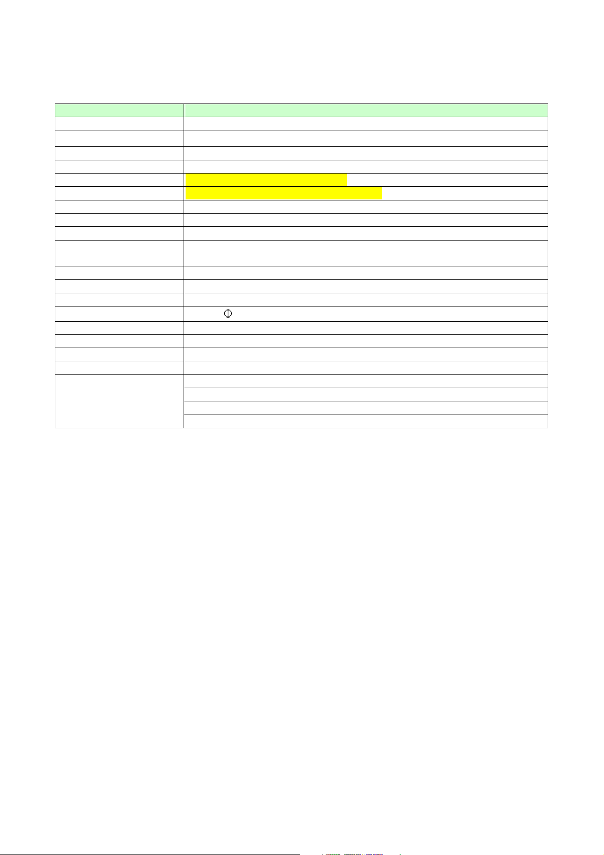
RSSI (7 Level, ‘no service, 0, 1, 2, 4, 5, 7’)
Battery Indicator (4 Level, 0~3)
Battery
Indicator
Antenna display (7 level settings and the corresponding RSSI)
Icons Indicator
Others reference to "Phone Personalization Setting"
FR/EFR/HR/AMR
Number of Keys: 48 Key (include 37 QWERTY keys, 4 function keys, 5 way
navigation keys, 2 side keys)
Soft Function Keys : 2
International Access (+)
User Selectable and Customizable Profiles (4 profiles: Normal, Outdoor, Silent,
Flight mode)
Key Tone
Key Tone Volume (6 Level - 0 ~ 5, 0 for Mute)
Key tone setting (DTMF, English)
Ring Tone
Ring Tone Volume (6 Level - 0 ~ 5, 0 for Mute)
Built-in Ring Tone Pattern: 20
Customizable Ring Tone Link: 5
Alert Type
5 Types - Ring, Vibration Only, Vibration and Ring, Ring after vibration, Silent
Power on/off tones
Built-in Ring Tone Pattern: 3 (include Silent) Built-in Ring Tone Pattern: 4
Power Off Tone
Built-in Ring Tone Pattern: 3 (include Silent)
Message Tone
Battery Indicator Voltage
3 -> 2
2 -> 1
1 -> 0
3.85
3.75
3.68
±±±±
0.05V
±±±±
0.05 V
±±±±
0.05 V
-7-
Personalization
Information
Management
Tools and
Utilities
Built-in Ring Tone Pattern: 8 (include Silent) 7
Warning Tone
Built-in Ring Tone Pattern: 1
Error Tone
Built-in Ring Tone Pattern: 1
Camp On Tone
Built-in Ring Tone Pattern: 1
Connect Tone
Built-in Ring Tone Pattern: 1
Status LED
Built-in Lighting Pattern: No (None, Pattern 1)
Charger-in Status LED
Built-in Lighting Pattern: No (None, Pattern 1)
Answer Mode
Any Key Answer, Send Key only
Auto (Only available for headset mode while headset plugged in) TBD
Calendar - Month view only Personal
To do list - 6 fields (Date, Start time, End time, Note, Alarm, Repeat)
Alarm
5 sets of Alarm
4 major fields for each set - On/Off, Time, Repeat type, Audio option
Phone
Setting
World Clock
Cities list: China(52),IND(54),CIS(68) cities
Daylight saving time support: activated by user selection
Home city set
Calculator
Addition, Subtraction, Multiplication, Division
Unit Converter
Weight, Length, Currency Converter
Memo
To do
Greeting Text
Shortcuts
Flight Mode
Time and Date Setting
Wallpaper
Sceen Saver
Power On Animation
Power Off Animation
LCD Backlight
-8-
PLMN/Service Indicator (Display of PLMN Name/Service Provider Name from SIM)
Date Time Display
Own Number Display
Restore Factory Default Setting
Security Phone Lock
SIM/Key Lock
Input Method
Engine
T9 (except Chinese)
Support Language
Depends on customer and market requirement.
Total supported languages will be limited to memory condition.
Predictive word input
Game
Java Games, provided by LGE.
Timer Teller Report the time by human voice every hour.
Support English, Chinese, Russian voices.
Anti-theft
Provide this feature by following LG spec. (GSM_VVLT 0 5_LMT_20071117_1.ppt)
Mobile Tracker
(ATMT)
2.2.3 GSM/GPRS Features
Function Target Specification
GPRS GPRS Multi slot Class 10
Data Service
Call History
(Dual SIM)
Call Cost
GPRS Counter
Call Management Call Swap
BS 24 - 26 (2400-9600 bit/s), asynchronous, non-transparent, UDI.
CSD rate up to 9.6K bit/s
Last Dialed Number: 80
Last Received Number: 80
Last Missed Number: 80
Scratch Pad Memory (Save an input number in call): 1
Last Call Time
Total Dialed Call Time
Total Received Call Time
Last Call Cost
Total Cost
Max Cost
Price Per Unit
Last Sent (unit in Byte)
Last Received (unit in Byte)
All Sent (unit in Byte)
All Received (unit in Byte)
-9-
ate
Call
Related Supplementary
Services
Phone Book
Call Retrieve
Automatic Redial
Speed Dialing
Last Number Redial
Support 40-digits Dialing Number from Idle, Phonebook in handset, and
Call Log
1. Idle dial screen: OK
2. Phonebook (Phone): OK
3. Phonebook (SIM): Have limitation, depend on SIM card.
4. Call Log: OK
5. SMS: support 20-digit
6. MMS: support 40-digit
Call Hold
Call Waiting
Calling Line Identity Presentation
Calling Line Identity Restriction
Connected Identification Restriction
Call Divert All voice Calls
Call Divert if unreachable
Call Divert if no answer
Call Divert if busy
Call Divert all data calls
Cancel all divert
Call Barring All Outgoing Calls
Call Barring All Outgoing International Calls
Call Barring All outgoing International except home
Call Barring All incoming Calls
Call Barring All incoming Calls when roaming
Multi-party Call (up to 7 calls, 5 in conference, 1 on held, 1 waiting)
Line switching (Line1, Line2)
Call reminder (Off, Single, Periodic)
Closed User Group
Quick Search (Notice: Quick search function only works in Phonebook,
SMS and MMS. In other application, this phone supports regular search.)
Alpha Store and Recall
Access Phone Book in call
Copy & Move
Fixed Dial Number
Service Dial Number
Speed Dial Number
SOS Number
Phone Entry: 1000 names (11 fields –Name, Mobile, Home, Office
number, Fax number, Email Address, Group, Associate Picture, Associ
Video, Associate Sound, Memo)
SIM Entry: 250 names (2 fields – Name, Mobile) TBC
-10-
Message Indication Type refer to
Caller Group-5 caller group- Friends, Family, VIP, Business, Others (6
fields – Name, Ring, Picture, LED pattern, Video, Member list)
Own Numbers: User can change the own numbers of handset. (Sets of
own numbers depends on SIM)
vCard:
Note: This phone doesn’t support phone number search.
Message
SMS
Standard SMS
SMS Reply Path
SMS Delivery Report
Valid period (1 hour/12 hours/1 day/1 week/Maximum)
Message Type (Text, Fax, Page, Email)
GSM 03.40
Basic text-only SMS as described in 3GPP TS 23.040 R5
Notice: This phone doesn’t support video ring tone via SMS
SMS Character Sets Support
GSM7
UCS-2
EMS
EMS Standard as described in 3GPP TS 23.040 R5 excluding WVG
EMS Text Format
Text Style: Normal, Bold, Italic, Underlined, Strikethrough
Text Alignment: Left, Right, Center
Text Size: Normal, Large, Small
EMS Image Support
1-bit small image 16x16 pixels black and white
1-bit large image 32x32 pixels black and white
1-bit variable image in single SMS packet
Extended black and white 1-bit image up to 255x255 pixels
Extended 6-bit image up to 255x255
Pre-defined animation
User-defined small animation 8x8 pixel 4-frame black and white
User-defined large animation 16x16 pixel 4-frame black and white
Pre-defined sound
User-defined i-Melody up to 128 bytes
LZSS compression algorithm
Re-use extended object
Object Distribution
User Prompt Indicator
Hyperlink format element
Extended Object Distribution
-11-

Notice: This mobile doesn’t support Nokia smart message format
(including WBMP), only support *.ems format" subject to Nokia smart
message license
EMS Character Sets Support
GSM7
UCS-2
EMS Miscellaneous
SMS Concatenation ( 8 Segments for MT/MO)
SMS Compression
MMS
MMS Standard as described in 3GPP TS 23.140 V4.8.0
Extract media from Message
Insert Media into message
OTA provisioning partially support (Network Profile setting
Auto download mode
Manual download mode
Operator can pre-configure the delivery mode
MMS notification with icon or Pop-up message display)
MMS Message Format
MMS SMIL (A subset of SMIL descried in the MMS Conformance
Document 1.2)
- maximal size for each MMS is limited by300KB
MMS Character Sets Support
US-ASCII
Unicode
ISO-8859-1
UTF-16
UTF-8
MMS Images Support
WBMP Wireless bitmap
GIF87
GIF89a
JPEG
MMS Sound Formats Support
WAV
AMR
MIDI
MP3
i-Melody
MMS Miscellaneous
Multipart binary MIME
-12-
Cell Broadcast
Network
SIM
Common Operation
Write Message
Read Message
Edit Message
(For MMS, Edit only conformance messages, unknown media not
supported, unknown SMIL not supported)
Reply Message
Send Message
Delete Message
Forward Message
Use Sender's Number
Message Templates
Extract media from Message (MMS/EMS)
Store Media (MMS/EMS)
Delete Media (MMS/EMS)
Read Cell Broadcast
Cell Broadcast Mode: Receive On/Off
Cell Broadcast Message Language
Channel Setting
Automatic Network Selection
Manual Network Selection
Network Service Status
Preferred Network (User definition)
GPRS connection mode selection: Always, When Needed
Common Operation
SIM Application Toolkit (Release 98 Class 2 certified)
Security
PIN
Personalization (Service provider lock, Network lock)
DTMF Signaling DTMF
DTMF Enable & Disable
-13-
2.2.4 Multimedia Features
Function Target Specification
Camera
Image size:
320X240, 640X480, 1280X1024
Zoom: 1x ~ 4x
Image Quality:
Super fine, Fine, Normal
White Balance:
Auto, Daylight, Tungsten, Fluorescent, Cloud, Incandescence
Shot: Three Shot Sounds
EV: -4 ~+4
Screen Mode:
Auto, Night
Banding: 60Hz/50Hz
Effect settings: (Total 14 7 types)
Normal, Grayscale, Sepia, Sepia Green, Sepia Blue,
Color Invert,
Storage Selection:
Phone, Memory card
(Only available when external memory card supported)
Image Viewer
Delay timer:
Off/ 3/ 5/ 10 Sec
Thumbnail supported
Browse Style:
List, Matrix
View
Forward:
To Wallpaper, Phonebook, Picture ID, MMS, Bluetooth
Rename
Delete
Delete All
Sort:
By Name, Type, Time, Size, None
Storage Selection:
Get list from Phone, Memory card
(Only available when external memory card supported)
Image Format Support
JPEG Baseline
GIF87a
GIF89a
WBMP
-14-

BMP
Music Player
Play
Pause
Resume
Stop
Next
Previous
Fast forward
Rewind
Storage Selection:
Get list from Phone, Memory card
(Only available when external memory card supported)
Auto-Generate Playlist
Skin: 2 skins
Repeat Mode:
Off, One Song, All Songs ,All off
Shuffle Play
Background Play
Equalizer Setting: 8 sets
Normal, Bass, Dance, Classical, Treble, Party, Pop, Rock
Video Player
Volume Control:
21 level (0~20, 0 for Mute)
Playlist Edit:
Add, Remove, Remove All
Sound Format Support
MP3
AMR
MIDI
WAV
AAC
Play
Pause
Stop
Fast forward
Rewind
Forward:
To MMS, Bluetooth
Rename
Delete
Delete All
-15-
Video Recorder
Sort:
By Name, Type, Date
Storage Selection:
Get list from Phone, Memory card
Volume Control:
21 level (0~20, 0 for Mute)
White Balance:
Auto, Daylight, Tungsten, Fluorescent, Cloud, Incandescence
EV: -4 ~+4
Night Mode:
On/Off
Banding: 60Hz/50Hz
Video Quality:
Super fine, Fine, Normal
Record Audio:
On/Off
Encode Format:
MPEG4, H.263
Sound Recorder
Effect settings: (Total 14 7 types)
Normal, Grayscale, Sepia, Sepia Green, Sepia Blue,
Color Invert,
Storage Selection:
Phone, Memory card
(Only available when external memory card supported)
Record
Pause
Resume Recording
Stop
Storage Selection:
Phone, Memory card
(Only available when external memory card supported)
Encode Format:
WAV, AMR
Record
Pause
Resume Recording
Stop
Edit Melody Compose
Play
-16-
melody file,
FM Radio
Save
Instrument Selection: 10 types
Piano, Guitar, Violin, Saxophone, Steel Drums, Flute, Harmonica,
Trumpet, Music Box, Xylophone
Play Speed:
Fast, Normal, Slow
[Notice] Melody composer only support one instrument in one i
so the last chosen instrument will be used to play this imelody file
Frequencies: 87.5 ~ 108.0
Skin: 2 skins
User definable Preset Channel List
Channel Auto Search
Background Play
Record
Record Format:
AMR, WAV
Record Storage:
Phone, Memory Card
(Only available when external memory card supported)
Preset Channel List generated by auto search
JAVA
MIDP 2.0
CLDC 1.1
Memory Limit 2MB
Support JSR 139,118,120,135,185
2.2.5 Connectivity Features
Function Target Specification
WAP
WAP 2.0 Spec.
WAP Push OTA/Message
WAP Provisioning Service
CSD/GPRS data connection
Bookmark
Wireless Telephony Application (WTA) support:
Only Public WTA support, supported functions listing below * Make a telephone call
* Send a string of DTMF tones over an established voice connection
* Add an entry to the telephone book of the device
Support OTA push and push message
OTA Provisioning & OTA download
Supports WML, WCSS, XHTML mp
Version 2.0 (w/o EDR) Bluetooth
Profile: GAP,SDAP,DUN,SPP,HSP,HFP,OPP,FTP,A2DP, AVRCP, BPP
Mass Storage Device 2.0 USB
Virtual COM
-17-
3. TECHNICAL BRIEF
3.1 Digital Main Processor
Figure.3-1-1 MT6235 FUNCTIONAL BLOCK DIAGRAM
3.1.1 System Overview
MT6235 is a highly-integrated and extremely powerful single-chip solution for
GSM/GPRS/EDGE mobile phones.
Based on the 32-bit ARM926EJ-STM RISC processor, MT6235’s superb processing power,
along with high bandwidth architecture and dedicated hardware support, provides an
unprecedented platform for high performance GPRS/EDGE Class 12 MODEM application.
Overall, MT6235 presents a revolutionary platform for mobile devices.
.
Platform
MT6235 is capable of running the ARM926EJ-STM RISC processor at up to 208 MHz, thus
providing fast data processing capabilities. In addition to the high clock frequency, separate
CODE and DATA caches are also included to further improve the overall system efficiency.
For large amounts of data transfer, high performance DMA (Direct Memory Access) with
hardware flow control is implemented, which greatly enhances the data movement speed while
reducing MCU processing load.
Targeted as a high performance platform for mobile applications, hardware flash content
protection is also provided to prevent unauthorized porting of the software load to protect the
manufacturer’s development investment.
-18-

Memory
To provide the greatest capacity for expansion and maximum bandwidth for data intensive
applications such as multimedia features, MT6235 supports up to 4 external state-of-the-art
devices through its 8/16-bit host interface. High performance devices such as Mobile SDRAM
and Cellular RAM are supported for maximum bandwidth. Traditional devices such as
burst/page mode flash, page mode SRAM, and Pseudo SRAM are also supported. For greatest
compatibility, the memory interface can also be used to connect to legacy devices such as
Color/Parallel LCD, and multi-media companion chips are all supported through this interface.
To minimize power consumption and ensure low noise, this interface is designed for flexible I/O
voltage and allows lowering of the supply voltage down to 1.8V. The driving strength is
configurable for signal integrity adjustment.
Multi-media
The MT6235 multi-media subsystem provides a connection to a CMOS image sensor and
supports a resolution up to 2.0 Mpixels. With its high performance application platform, MT6235
allows efficient processing of image and video data.
In addition to image and video features, MT6235 utilizes high resolution DAC, digital audio,
and audio synthesis technology to provide superior audio features for all future multi-media
needs.
Connectivity and Storage
To take advantage of its incredible multimedia strengths, MT6235 incorporates myriads of
advanced connectivity and storage options for data storage and communication. MT6235
supports UART, Fast IrDA, USB 2.0, SDIO, Bluetooth, Touch Screen Controller, WIFI Interface,
and MMC/SD/MS/MS Pro storage systems. These interfaces provide MT6235 users with the
highest degree of flexibility in implementing solutions suitable for the targeted application.
To achieve a complete user interface, MT6235 also brings together all the necessary
peripheral blocks for a multi-media GSM/GPRS/EDGE phone. The peripheral blocks include
the Keypad Scanner with the capability to detect multiple key presses, SIM Controller, Alerter,
Real Time Clock, PWM, Serial LCD Controller, and General Purpose Programmable I/Os.
Furthermore, to provide much better configurability and bandwidth for multi-media products,
an additional 18-bit parallel interface is incorporated. This interface enables connection to LCD
panels as well as NAND flash devices for additional multi-media data storage.
Audio
Using a highly integrated mixed-signal Audio Front-End, the MT6235 architecture allows for
easy audio interfacing with direct connection to the audio transducers. The audio interface
integrates D/A and A/D Converters for Voice band, as well as high resolution Stereo D/A
Converters for Audio band. In addition, MT6235 also provides Stereo Input and Analog MUX.
MT6235 supports AMR codec to adaptively optimize speech and audio quality. Moreover,
HE-AAC codec is implemented to deliver CD-quality audio at low bit rates.
On the whole, MT6235’s audio features provide a rich solution for multi-media applications.
Radio
MT6235 integrates a mixed-signal baseband front-end in order to provide a well-organized
radio interface with flexibility for efficient customization. The front-end contains gain and offset
calibration mechanisms, and filters with programmable coefficients for comprehensive
compatibility control on RF modules. This approach allows the usage of a high resolution D/A
Converter for controlling VCXO or crystal, reducing the need for an expensive TCVCXO.
MT6235 achieves great MODEM performance by utilizing a 14-bit high resolution A/D
-19-

Converter in the RF downlink path. Furthermore, to reduce the need for extra external
current-driving component, the driving strength of some BPI outputs is designed to be
configurable.
Debug Function
The JTAG interface enables in-circuit debugging of the software program with the
ARM926EJ-S core. With this standardized debugging interface, MT6235 provides
developers with a wide set of options in choosing ARM development kits from different third
party vendors.
Power Management
The MT6235 offers various low-power features to help reduce system power consumption.
These features include a Pause Mode of 32 KHz clocking in Standby State, Power Down Mode
for individual peripherals, and Processor Sleep Mode. MT6235 is also fabricated in an
advanced low leakage CMOS process, hence providing an overall ultra low leakage solution.
Package
The MT6235 device is offered in a 13mm×13mm, 362-ball, 0.5 mm pitch, TFBGA package.
3.1.2 Platform Features
General
Integrated voice-band, audio-band and base-band analog front ends
TFBGA 13mm×13mm, 362-ball, 0.5 mm pitch package
MCU Subsystem
ARM926EJ-S 32-bit RISC processor
High performance multi-layer AMBA bus
Java hardware acceleration for fast Java-based games and applets
Operating frequency: 26/52/104/208 MHz
Dedicated DMA bus
14 DMA channels
512K bits on-chip SRAM
384K bits Instruction-TCM
640K bits Data-TCM
128K bits Instruction-Cache
128K bits Data-Cache
On-chip boot ROM for Factory Flash Programming
Watchdog timer for system crash recovery
3 sets of General Purpose Timer
Circuit Switch Data coprocessor
Division coprocessor
PPP Framer coprocessor
External Memory Interface
Supports up to 4 external memory devices
Supports 8-bit or 16-bit memory components with maximum size of up to 128M Bytes each
Supports Mobile SDRAM and Cellular RAM
Supports Flash and SRAM/PSRAM with page mode or burst mode
Industry standard Parallel LCD interface
-20-

Supports multi-media companion chips with 8/16 bits data width
Flexible I/O voltage of 1.8V ~ 2.8V for memory interface
Configurable driving strength for memory interface
User Interfaces
8-row × 8-column keypad controller with hardware scanner
Supports multiple key presses for gaming
SIM/USIM controller with hardware T=0/T=1 protocol control
Real Time Clock (RTC) operating with a separate power supply
General Purpose I/Os (GPIOs)
4 sets of Pulse Width Modulation (PWM) output
Alerter output with Enhanced PWM or PDM
8 external interrupt lines
Security
Supports security key and 126 bit chip unique ID
Connectivity
3 UARTs with hardware flow control and speeds up to 921600 bps
IrDA modulator/demodulator with hardware framer. Supports SIR/MIR/FIR operating speeds.
USB 2.0 capability
Multi Media Card, Secure Digital Memory Card, Memory Stick, Memory Stick Pro host
controller with flexible I/O voltage power
Supports SDIO interface for SDIO peripherals as well as WIFI connectivity
DAI/PCM and I2S interface for Audio application
Power Management
Power Down Mode for analog and digital circuits
Processor Sleep Mode
Pause Mode of 32 KHz clocking in Standby State
4-channel Auxiliary 10-bit A/D Converter for charger and battery monitoring and photo
sensing
Test and Debug
Built-in digital and analog loop back modes for both Audio and Baseband Front-End
DAI port complying with GSM Rec.11.10
JTAG port for debugging embedded MCU
3.1.3 MODEM Features
Radio Interface and Baseband Front End
GMSK modulator with analog I and Q channel outputs
10-bit D/A Converter for uplink baseband I and Q signals
14-bit high resolution A/D Converter for downlink baseband I and Q signals
Calibration mechanism of offset and gain mismatch for baseband A/D Converter and D/A
Converter
10-bit D/A Converter for Automatic Power Control
13-bit high resolution D/A Converter for Automatic Frequency Control
Programmable Radio RX filter
2 channels Baseband Serial Interface (BSI) with 3-wire control
-21-

Bi-directional BSI interface. RF chip register read access with 3-wire or 4-wire interface.
10-Pin Baseband Parallel Interface (BPI) with programmable driving strength
Multi-band support
Voice and Modem CODEC
Dial tone generation
Voice memo
Noise reduction
Echo suppression
Advanced sidetone Oscillation Reduction
Digital sidetone generator with programmable gain
Two programmable acoustic compensation filters
GSM/GPRS quad vocoders for adaptive multirate (AMR), enhanced full rate (EFR), full rate
(FR) and half rate (HR)
GSM channel coding, equalization and A5/1, A5/2 and A5/3 ciphering
GPRS GEA1, GEA2 and GEA3 ciphering
Programmable GSM/GPRS/EDGE modem
Packet Switched Data with CS1/CS2/CS3/CS4 coding schemes
GSM Circuit Switch Data
GPRS/EDGE Class 12
Voice Interface and Voice Front End
Two microphone inputs sharing one low noise amplifier with programmable gain and
automatic
gain control (AGC) mechanisms
Voice power amplifier with programmable gain
2nd order Sigma-Delta A/D Converter for voice uplink path
D/A Converter for voice downlink path
Supports half-duplex hands-free operation
Compliant with GSM 03.50
3.1.4 Multi-Media Features
LCD/NAND Flash Interface
Dedicated Parallel Interface supports 3 external devices with 8-/16-bit NAND flash interface,
8-/9-/16-/18-bit Parallel interface, and Serial interface for LCM
Built-in NAND Flash Controller with 1-bit ECC for mass storage
LCD Controller
Supports simultaneous connection to up to 3 parallel LCD and 2 serial LCD modules
Supports LCM format: RGB332, RGB444, RGB565, RGB666, RGB888
Supports LCD module with maximum resolution up to 800x600 at 24bpp
Per pixel alpha channel
True color engine
Supports hardware display rotation
Capable of combining display memories with up to 6 blending layers
Image Signal Processor
8 bit YUV format image input
Capable of processing image of size up to 2.0 M pixels
-22-

IEEE Std 1180-1990 IDCT standards compliance
Supports progressive image processing to minimize storage space requirement
Supports reload-able DMA for VLD stream
Image Data Processing
Supports Digital Zoom
Supports RGB888/565, YUV444 image processing
High throughput hardware scaler. Capable of tailoring an image to an arbitrary size.
Horizontal scaling in averaging method
Vertical scaling in bilinear method
YUV and RGB color space conversion
Boundary padding
2D Accelerator
Supports 32-bpp ARGB8888, 24-bpp RGB888, 16-bpp RGB565, and 8-bpp index color
modes
Supports SVG Tiny
Rectangle gradient fill
BitBlt: multi-BitBlt with 7 rotation, 16 binary ROP
Alpha blending with 7 rotation
Line drawing: normal line, dotted line, anti-aliasing
Circle drawing
Bezier curve drawing
Triangle flat fill
Font caching: normal font, italic font
Command queue with max depth of 2047
Audio CODEC
Supports HE-AAC codec decode
Supports AAC codec decode
Wavetable synthesis with up to 64 tones
Advanced wavetable synthesizer capable of generating simulated stereo
Wavetable including GM full set of 128 instruments and 47 sets of percussions
PCM Playback and Record
Digital Audio Playback
Audio Interface and Audio Front End
Supports I2S interface
High resolution D/A Converters for Stereo Audio
Stereo analog input for stereo audio source
Analog multiplexer for stereo audio
Stereo to mono conversion
-23-

3.1.5 General Description
Figure 3-1-2 depicts the block diagram of MT6235. Based on a dual-processor architecture,
MT6235 integrates both an ARM926EJ-S core and a digital signal processor core.
ARM926EJ-S is the main processor responsible for running high-level GSM/GPRS protocol
software as well as multi-media applications. The digital signal processor manages the
low-level MODEM as well as advanced audio functions. Except for a few mixed-signal
circuitries, the other building blocks in MT6235 are connected to either the microcontroller or
the digital signal processor.
MT6235consists of the following subsystems:
Microcontroller Unit (MCU) Subsystem:
Includes an ARM926EJ-S RISC processor and its accompanying memory
management and interrupt handling logics;
Digital Signal Processor (DSP) Subsystem:
Includes a DSP and its accompanying memory, memory controller, and interrupt
controller;
MCU/DSP Interface:
The junction at which the MCU and the DSP exchange hardware and software
information;
Microcontroller Peripherals:
Includes all user interface modules and RF control interface modules;
Microcontroller Coprocessors:
Runs computing-intensive processes in place of the Microcontroller;
DSP Peripherals:
Hardware accelerators for GSM/GPRS/EDGE channel codec;
Multi-media Subsystem:
Integrates several advanced accelerators to support multi-media applications;
Voice Front End:
The data path for converting analog speech to and from digital speech;
Audio Front End:
The data path for converting stereo audio from an audio source;
Baseband Front End:
The data path for converting a digital signal to and from an analog signal from the RF
modules;
Timing Generator:
Generates the control signals related to the TDMA frame timing;
Power, Reset and Clock Subsystem:
Manages the power, reset, and clock distribution inside MT6235.
-24-
Figure.3-1-2 MT6235 BLOCK DIAGRAM
-25-
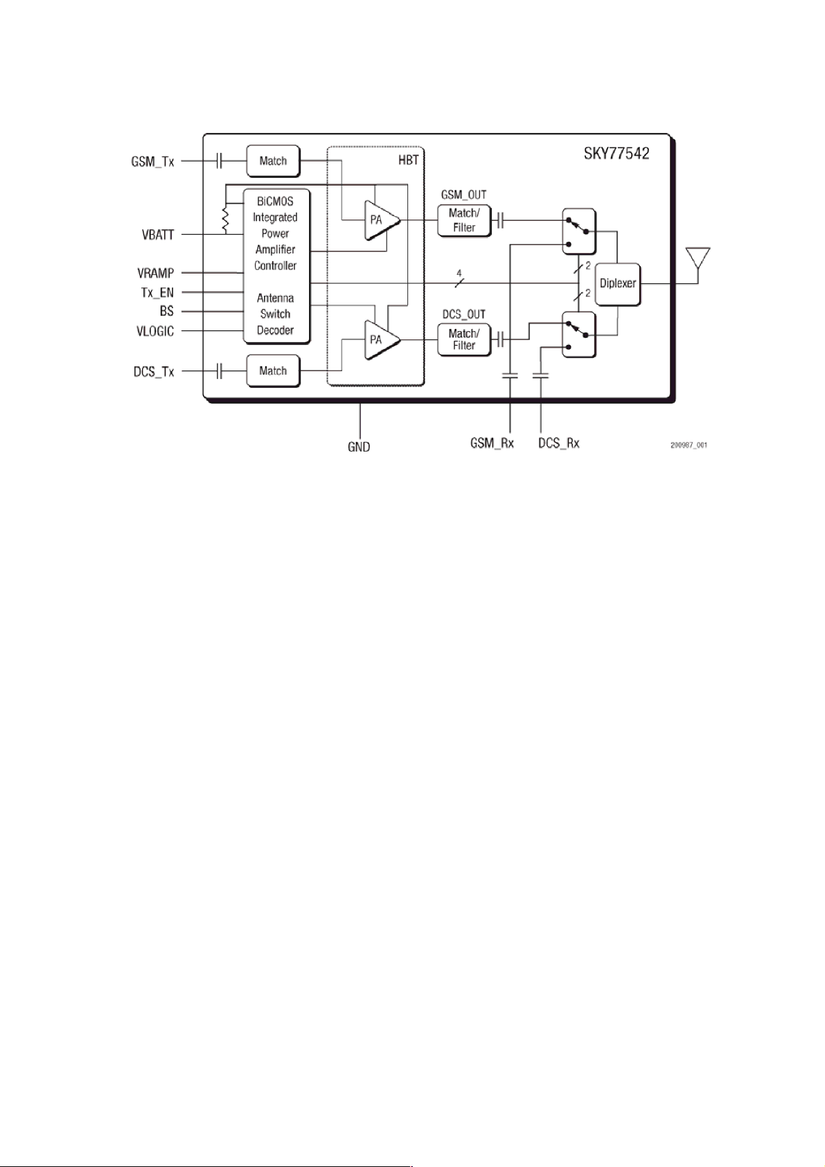
3.2 Power Amplifier Module (SKY77542)
Figure.3-2-1 SKY77542 FUNCTIONAL BLOCK DIAGRAM
The SKY77542 is a transmit and receive front-end module (FEM) with Integrated Power
Amplifier Control (iPAC.) for dual-band cellular handsets comprising GSM900 and DCS1800
operation.Designed in a low profile, compact form factor, the SKY77542 offers a complete
Transmit VCO-to- Antenna and Antenna-to-Receive SAW filter solution. The FEM also supports
Class 12 General Packet Radio Service (GPRS) multi-slot operation.
The module consists of a GSM900 PA block and a DCS1800 PA block,
impedance-matching circuitry for 50 Ω input and output impedances, Tx harmonics filtering,
high linearity and low insertion loss PHEMT RF switches, diplexer and a Power Amplifier
Control (PAC) block with internal current sense resistor. A custom BiCMOS integrated circuit
provides the internal PAC function and decoder circuitry to control the RF switches. The two
Heterojunction Bipolar Transistor (HBT) PA blocks are fabricated onto a single Gallium
Arsenide (GaAs) die. One PA block supports the GSM900 band and the other PA block
supports the DCS1800 band. Both PA blocks share common power supply pads to distribute
current. The output of each PA block and the outputs to the two receive pads are connected to
the antenna pad through PHEMT RF switches and a diplexer. The GaAs die, PHEMT die,
Silicon (Si) die and passive components are mounted on a multi-layer laminate substrate. The
assembly is encapsulated with plastic overmold.
Band selection and control of transmit and receive modes are performed using two external
control pads. Refer to the functional block diagram in Figure 3-2-1 below. The band select pad
(BS) selects between GSM and DCS modes of operation. The transmit enable (Tx_EN) pad
controls receive or transmit mode of the respective RF switch (Tx = logic 1). Proper timing
between transmit enable (Tx_EN) and Analog Power Control (VRAMP) allows for high isolation
between the antenna and Tx-VCO while the VCO is being tuned prior to the transmit burst.
-26-
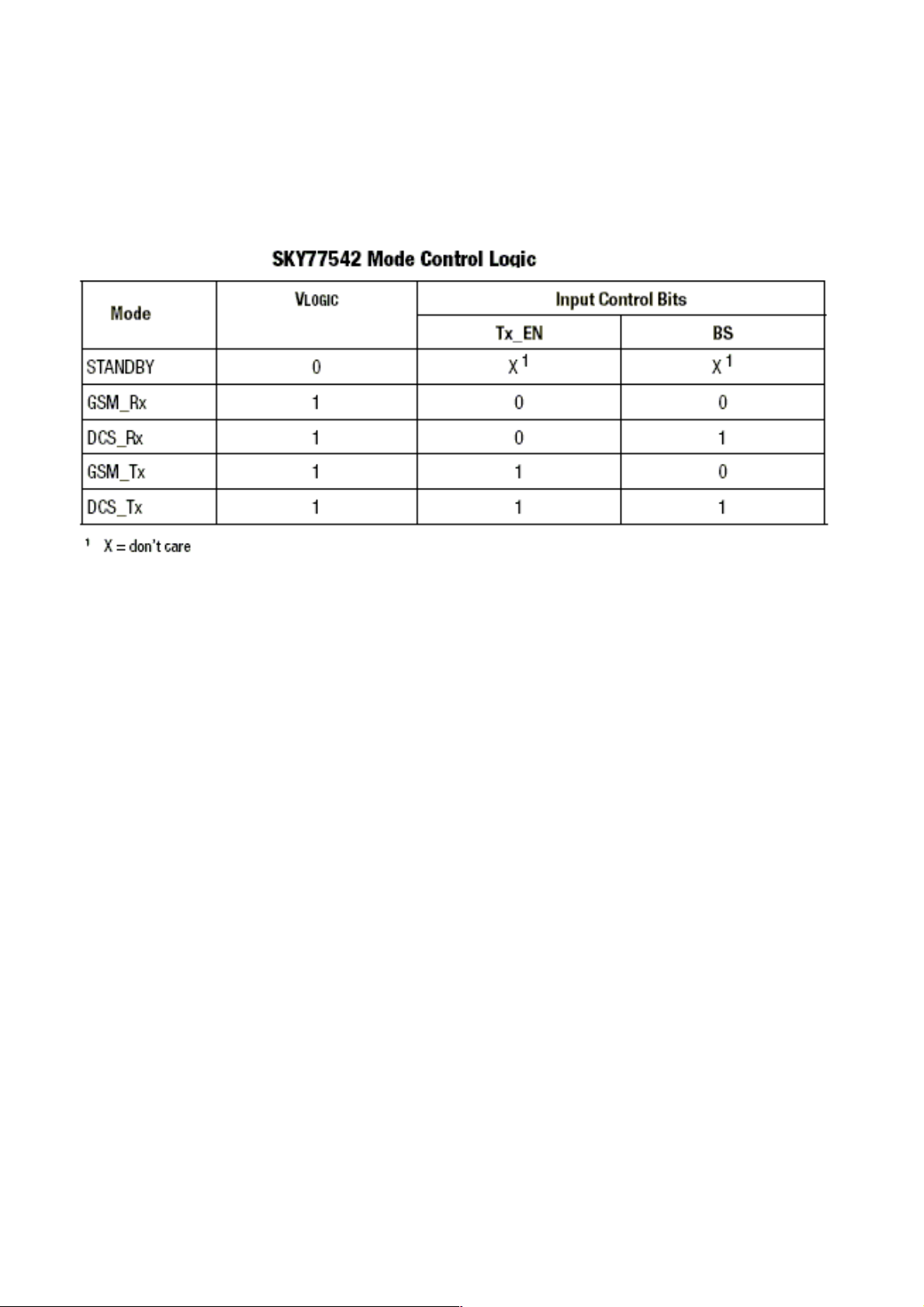
The SKY77542 is compatible with logic levels from 1.2 V to VCC for BS and Tx_EN pads,
depending on the level applied to the VLOGIC pad. This feature provides additional flexibility for
the designer in the selection of FEM interface control logic.
-27-
3.3 Transceiver Module (AD6548)
Figure.3-3-1 AD6548 FUNCTIONAL BLOCK DIAGRAM
3.3.1 General Descriptions
The AD6548/9 provides a highly integrated direct conversion radio solution that combines, on
a single chip, all radio and power management functions necessary to build the most compact
GSM radio solution possible. The only external components required for a complete radio
design are the Rx SAWs, PA, Switchplexer and a few passives enabling an extremely small
cost effective GSM Radio solution.
The AD6548/9 uses the industry proven direct conversion receiver architecture of the
OthelloTM family. For Quad band applications the front end features four fully integrated
programmable gain differential LNAs. The RF is then downconverted by quadrature mixers and
then fed to the baseband programmable-gain amplifiers and active filters for channel selection.
The Receiver output pins can be directly connected to the baseband analog processor. The
Receive path features automatic calibration and tracking to remove DC offsets.
The transmitter features a translation-loop architecture for directly modulating baseband
signals onto the integrated TX VCO. The translation-loop modulator and TX VCO are extremely
low noise removing the need for external SAW filters prior to the PA.
The AD6548/9 uses a single integrated LO VCO for both the receive and the transmit circuits.
The synthesizer lock times are optimized for GPRS applications up to and including class 12.
To dramatically reduce the BOM both TX Translational loop and main PLL Loop Filters are fully
integrated into the device.
AD6548 incorporates a complete reference crystal calibration system. This allows the
external VCTCXO to be replaced with a low cost crystal. No other external components are
required. The AD6549 uses the traditional VCTCXO reference source.
The AD6548/9 also contains on-chip low dropout voltage regulators (LDOs) to deliver
regulated supply voltages to the functions on chip, with a battery input voltage of between 2.9V
-28-
and 5.5V. Comprehensive power down options are included to minimize power consumption in
normal use.
A standard 3 wire serial interface is used to program the IC. The interface features
low-voltage digital interface buffers compatible with logic levels from 1.6V to 3.0V.
The AD6548/9 is packaged in a 5mm × 5mm , 32-lead LFCSP package.
ORDERING GUIDE Model TemperatureRange Package
AD6548BCPZ
-20°C to +85°C
LFCSP-32
AD6549BCPZ -20°C to +85°C LFCSP-32
3.3.2 Features
Fully Integrated GSM Transceiver including
Direct Conversion Receiver
4 Differential LNAs
Integrated Active RX Channel Select Filters
Programmable Gain Baseband Amplifiers
Translation Loop Direct VCO Modulator
Integrated TX VCO and tank
External TX filters eliminated
Integrated Loop filter components
High performance multi band PLL system
Fast Fractional-N Synthesizer
Integrated Local Oscillator VCO
Fully Integrated Loop filters
Crystal Reference Oscillator & Tuning System (AD6548)
Power Management
Integrated LDOs allow direct battery supply connection
Small footprint
32-Lead 5 X 5 mm Chipscale Package
APPLICATIONS
Dual, Triple and Quad Band Radios
- GSM850, E-GSM 900, DCS1800 and PCS1900
- GPRS to Class 12- EDGE RX
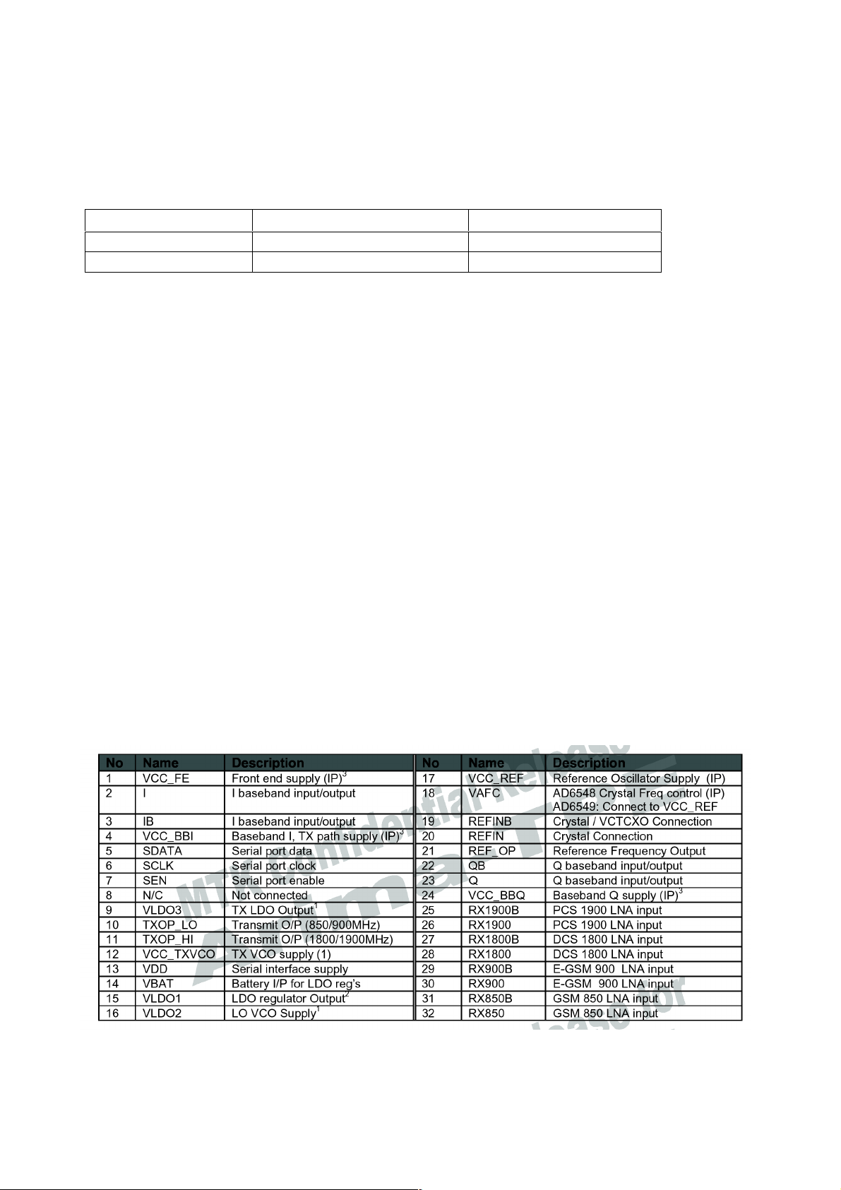
3.3.3 Pin Descriptions
-29-

3.4 Bluetooth Module (MTK_MT6612)
3.4.1 General description
Bluetooth is a low-cost wireless technology used to provide “ad hoc” networking between
versatile portable devices such as cell phones, PDAs, digital cameras, headsets, and more.
MT6612 is a highly integrated Bluetooth platform IC. It includes powerful baseband
processing capabilities with rich features and a high performance transceiver, all in a compact
single package.
3.4.2 Features
Radio features
Fully compliant with Bluetooth specification 2.1+ EDR
Low out-of-band spurious emissions supports simultaneous operation with GPS, GSM/GPRS
worldwide radio systems.
Low-IF architecture with high degree of linearity and high order filter
Intergrated T/R switch.
Transmitter features
Meets class 2 and class 3 transmitting requirement.
Fully integrated PA provides 9 dBm output power (antenna out)
Receiver features
-91dBm sensitivity with excellent interference rejection performance.
Hardware AGC dynamically adjusts receiver performance in changing environments.
Baseband features
Up to 7 simultaneous active ACL links
Up to 3 simultaneous SCO and eSCO link with CVSD coding
eSCO support.
Scatternet support: Up to 4 piconets simultaneously with background inquiry/page scan.
Sniff mode, hold mode, and part mode support.
AFH and PTA collaborative support for WLAN/BT coexistence.
Idle mode and sleep mode enables ultra low power consumption
PCM interface and built-in transcoders for A-law, µ-law and linear voice.
Built-in hardware modem engine for access code correlation, header error correction, forward
error correction,CRC, whitening, and encryption.
Channel quality driven data rate adaptation.
Channel assessment for AFH
Platform features
Integrated LDO enables direct connection to battery.
Wide ranges of crystal and external reference clock support.
High speed UART support.
Built-in RAM and ROM with patch system.
External LPO clock support for sleep mode.
Supports standard HCI interface.
Capable to support Bluetooth 2.1 features.
Provides USB full-speed device function
Support a SPI interface to access externa; serial flash and EEPROM
Embedded 128-bit effuse for Bluetooth Address use
-30-
 Loading...