

LG X220ds SERVICE MANUAL
MOBILE PHONE
SERVICE MANUAL
CAUTION
BEFORE SERVICING THE UNIT, READ THE “SAFETY PRECAUTIONS” IN THIS MANUAL
MODEL : LG-X220ds
Internal Use Only
Date: Apr, 2016 / Issue 1.0

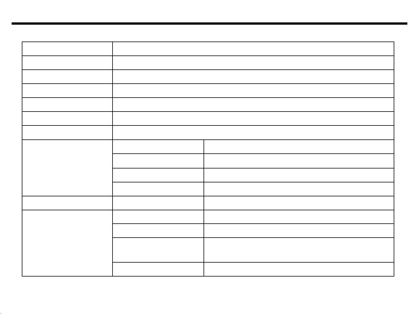
Table Of Contents
2
1. INTRODUCTION................................................. 3
1.1 Purpose
1.2 Regulatory Information
2. PERFORMANCE................................................... 4
2.1 Band Specification
2.2 HW Features
2.3 RSSI Display
2.4 Current consumption
2.5 Battery bar
2.6 SW Specification
3. TROUBLE SHOOTING..........................................12
3.1 Checking XO Block
3.2 Checking Transceiver DC Power Supply Circuit Block
3.3 FEM (Front-End Module) Block
3.4 GSM RF PART
3.5 WCDMA RF Part
3.6 Connectivity PART
3.7 Power
3.8 charger
3.9 Checking Audio Block
3.10 Checking LCD Block
3.11 Checking Touch Block
3.12 Checking sensor Block
3.13 Checking USB Block
3.14 Checking camera Block
6. BGA PIN MAP............................................................ 84
7. PCB LAYOUT…........................................................... 85
8. HIDDEN MENU.......................................................... 91
9. DOWNLOAD…........................................................... 94
10. CALIBRATION...........................................................95
11. DISASSEMBLE GUIDE............................................. 96
12. EXPLODED VIEW………………………………………... 98
13. REPLACEMENT PART LIST..…………………………. 99
4. BLOCK DIAGRAM…........................................... 56
5. CIRCUIT DIAGRAM............................................ 65
LGE Internal Use Only
Copyright ⓒ 2016 LG Electronics. Inc. All right
reserved. Only training and service purposes

1. INTRODUCTION
3
1.1 Purpose
This manual provides the information necessary to repair, calibration, description and download the features of this model.
1.2 Regulatory Information
A. Security
This material is prohibited to share and release to unauthorized person, in accordance with the regulations, LG Electronics, Civil / criminal
responsibility in accordance with the relevant provisions violate.
B. Precautions for repair
• In c
• When u
• When f
C. Attention
Boards, which contain Electrostatic Sensitive Device (ESD), are indicated by the sign.
Following information is ESD handling:
• Service personal should ground themselves by using a wrist, strap when exchange system board.
• When repair are made to a system board, they should spread the floor with anti-
• Use a suitable, grounded soldering iron.
• Keep sensitive parts in these protective packages until these are used.
• When returning system board or parts like EEPROM to the Factory, use the protective package as described.
ase of Disassembly or Assembly to repair product, be careful of a product failure caused by RF signals and Static electricity.
sing Magnetic tool for the Phone's SVC repair, you should check affect the Electric parts according to effect of Magnet.
astening the screw, be careful not to damage the head of screw and even product.
LGE Internal Use Only
static mat which is also grounded.
Copyright ⓒ 2016 LG Electronics. Inc. All right
reserved. Only training and service purposes

2.1 Band Specification
4
Support Band TX Freq (MHz) RX Freq (MHz)
2. PERFORMANCE
WCDMA(FDD1
)
WCDMA(FDD8
)
EGSM 880 – 915 925 – 960
GSM850 824 – 849 869 – 894
DCS1800 1710 – 1785 1805 – 1880
PCS1900 1850 – 1910 1930 – 1990
1920 – 1980 2110 – 2170
880 – 915 925 – 960
LGE Internal Use Only
Copyright ⓒ 2016 LG Electronics. Inc. All right
reserved. Only training and service purposes
2.2 HW Features
5
2. PERFORMANCE
List
1. Phone Type Bar Type
2. Size 141.5 x 71.6 x 8.9 mm
3. Weight 128g ( with Battery )
4. Battery 1,900mAh(Typ) (Li-Ion), 1,820mAh(Min.)
5.Chipset MT6580A/WM
6. Memory 8GB(EMMC) + 1GB(LPDDR3)External Memory(SD Card) : Up to 32GB
7. LCD Size 5 inch
8. Touch Type 5 inch Capacitive type
9. Main Camera (5M) Type CMOS image sensor
Type / Spec.
Display Type Active matrix TFT, Transmissive Type
Color 16.7M colors
Resolution 854(H) x 480(W) 196ppi
LGE Internal Use Only
Resolution
Image Scaling Down
Format Image : JPG, Video : MP4
2560(H) X 1920 (V) pixels.
5M(2560x1920), 4M(2560x1440), 3M(2048x1536), 2M(1600x1200),
1.3M(1280x960), 1M(1280x720)
Copyright ⓒ 2016 LG Electronics. Inc. All right
reserved. Only training and service purposes

2.2 HW Features
6
2. PERFORMANCE
10.Front Camera(2M)
11. Audio
12. Bluetooth Standard Bluetooth 4.1
13. WLAN Standard IEEE 802.11 b/g/n
Type CMOS image sensor
Resolution 2,560(H) x 1,920(V)
Format Image : JPG, Video : 3GP
Receiver/Speaker 2in1 18 X 10 X 3.1T Speaker
Format MP3, AAC, MIDI, EAAC+, OGG, AMR, AAC+, WAV, FLAC
Effective Distance 10M
Distance 0 m ~ 10 m (depend on environment)
Throughput Max 40Mbps (SDIO Driver performance)
Depend on environment 0 ~ 50m (depend on environment)
14. GPS type A-GPS
15. FM type FM Radio, 3.5pi Ear-jack
LGE Internal Use Only
Copyright ⓒ 2016 LG Electronics. Inc. All right
reserved. Only training and service purposes

2.3 RSSI Display
7
Antenna BAR
54 -85 ±3dBm -91 ±3dBm
43 -92 ±3dBm -96 ±3dBm
2. PERFORMANCE
Specification
Unit
WCDMA(RSCP) GSM(RSSI)
32 -98 ±3dBm -98 ±3dBm
21 -102 ±3dBm -102 ±3dBm
10 -106 ±3dBm -104 ±3dBm
2.4 Current consumption
Specification
Item
WCDMA GSM
1. Current(Sleep & Idle AVG) Under 6mA(@DRX7) Under 6mA(@PG 5)
≤340mA(@PCL5,GSM900/GSM8
2. Talking Current
≤260mA @10dBm
≤270mA @12dBm
50)
≤280mA(@PCL0,DCS1800/PCS1
900)
dBm
LGE Internal Use Only
Copyright ⓒ 2016 LG Electronics. Inc. All right
reserved. Only training and service purposes

2.5 Battery bar
8
2. PERFORMANCE
LGE Internal Use Only
Copyright ⓒ 2016 LG Electronics. Inc. All right
reserved. Only training and service purposes
2.6 SW Specification
9
Item Feature Comment
RSSI 0 ~ 5 Levels
Battery Charging 0 ~ 100%
Key Volume No No key volume setting
Audio Volume 0 ~ 15 Level
Time / Date Display Yes
Multi-Language Yes depending on build language
Quick Access Mode Phone / Contact / Browser / Messaging
PC Sync No
Speed Dial Yes Voice mail center -> 1 key
Profile No not same with feature phone setting
CLIP / CLIR Yes
Phone Book Name / Phonetic / Nickname / Photo / Phone / E
Last Dial Number Yes
Last Received Number Yes
Last Missed Number Yes
Search by Number/Name Yes
Group Yes There is no limitation on the number of it
mail / Postal addresses / Birthday / Company / N
otes / IM / Relationship
2. PERFORMANCE
There is no limitation on the number of it
ems.
It depends on available memory amount.
ems.
It depends on available memory amount.
Service Dial Number No
LGE Internal Use Only
Fixed Dial Number Yes
Own Number No My Profile (add/edit/delete are supporte
d)
Copyright ⓒ 2016 LG Electronics. Inc. All right
reserved. Only training and service purposes
2.6 SW Specification
There is no limitation on the number of items.
The
p the screen to easily turn it on or off.
10
Voice Memo Yes Support voice recorder
Call Reminder
etwork Selection Automatic
N
Mute Yes
Call Divert Yes
Call Barring Yes
Call Charge (AoC) No
Call Duration Yes
SMS (EMS)
SMS Over GPRS Yes
EMS Melody / Picture No
Send / Receive / Save
MMS MPEG4 Yes ØSend / Receive : Yes
Send / Receive / Save ØSave : depends on content type
2. PERFORMANCE
No
EMS does not support.
It depends on available memory amount.
Support video content type list
Long Message MAX 450 characters SMS
Cell Broadcast Yes
Download Over the Web
Game No
Calendar Yes
Memo No
World Clock Yes
Knock on Yes
LGE Internal Use Only
1.video/mp4
2.video/h263, h264
3.video/3gpp2
video/3gpp
Knock ON feature allows you to double-ta
Copyright ⓒ 2016 LG Electronics. Inc. All right
reserved. Only training and service purposes
2.6 SW Specification
Taking the photos with a gesture, There are tw
o methods for using the Gesture shot feature.
11
Unit Convert No
Stop Watch Yes
Wall Paper Yes
WAP Browser No Support only web browser based on webkit. W
Download Melody / Yes Over web browser
Wallpaper
SIM Lock No
SIM Toolkit Yes
MMS Yes Google MMS Client
EONS Yes
CPHS Yes V4.2
ENS No
Camera Yes 5M FF /
JAVA No
Voice Dial Yes US English only
IrDa No IrRC
Bluetooth Yes Ver. 4.1
FM radio Yes
GPRS Yes Class 12
EDGE Yes Class 12(Rx only)
Hold / Retrieve Yes
Conference Call Yes Max. 6
DTMF Yes
Memo pad No
TTY No
AMR Yes
SyncML Yes
IM Yes Google Hangout
Email Yes
LGE Internal Use Only
LGE Internal Use Only
Gesture shot Yes
2. PERFORMANCE
AP stack and wml are not supported.
Digital Zoom : x4
Copyright ⓒ 2016 LG Electronics. Inc. All right
reserved. Only training and service purposes

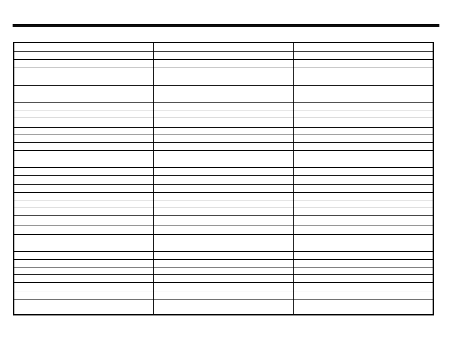
3.1 Checking XO Block
12
3. TROUBLE SHOOTING
The out put frequency(26.0MHz) of XO(X3101) is used as the reference one of MT6580 internal VCO
Image
Checking Flow
Main
Top
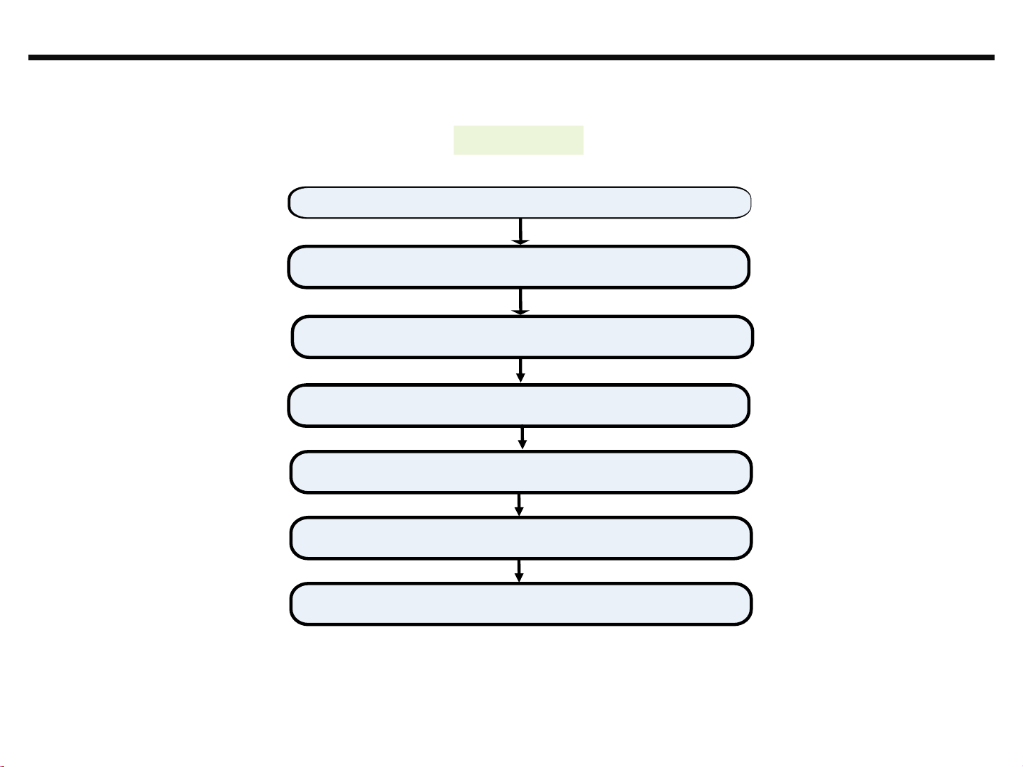
START
X3101
Check TP1
Is it 26.0 MHz?
NO
Replace X3101 and then
check TP1
Is it 26.0 MHz?
NO
The Problem may be Logic part
Refer to Logic trouble shoot
YES
YES
XO Circuit is OK.
TP1 (X3101)
Check next step
Circuit Diagram
XO Circuit is OK.
Check next step
TP1 (X3101)
LGE Internal Use Only
Copyright ⓒ 2016 LG Electronics. Inc. All right
reserved. Only training and service purposes
3.2 Checking Transceiver DC Power Supply Circuit Block
13
The MT6580 operating voltages used three voltage sources 1.8V and 1.8V and 2.8V
Checking Flow
START
Main
Top
3. TROUBLE SHOOTING
Image
U1001
TP2
TP3
Check TP1
+1.8V is OK?
YES
Check TP2
+1.8V is OK?
YES
Check TP3
+2.8V is OK?
Check next step
The Problem may be Logic part
Refer to Logic trouble shoot
NO
The Problem may be Logic part
Refer to Logic trouble shoot
NO
The Problem may be Logic part
Refer to Logic trouble shoot
NO
TP1
Circuit Diagram
TP3(2.8V)(C3121)
TP2(1.8V)(R3115)
TP1(1.8V)(R3123)
LGE Internal Use Only
Copyright ⓒ 2016 LG Electronics. Inc. All right
reserved. Only training and service purposes
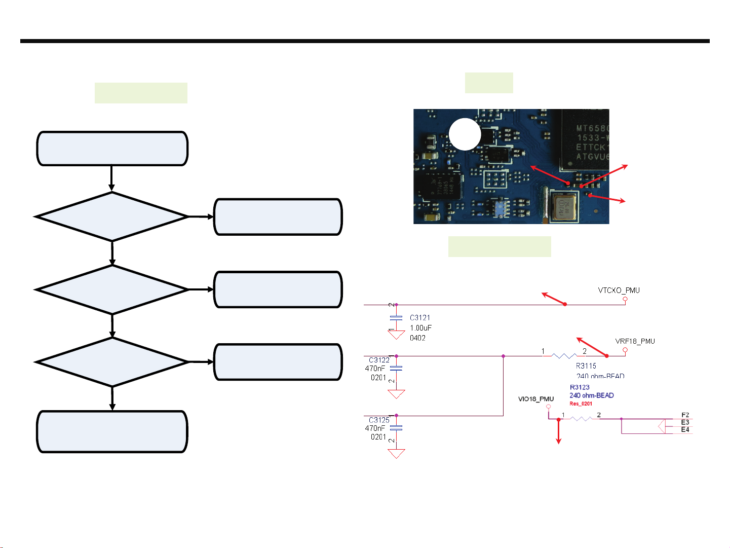
3.3 FEM (Front-End Module) Block
14
3.3.1 . FEM Mode Control Logic Table
FEM Mode Control Logic Table
3. TROUBLE SHOOTING
LGE Internal Use Only
Copyright ⓒ 2016 LG Electronics. Inc. All right
reserved. Only training and service purposes
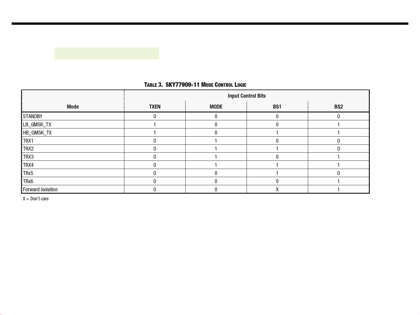
3.3 FEM (Front-End Module) Block
15
3.3.2 . All Band FEM Block (GSM 850/900/1800/1900, WCDMA B2/5)
Checking Flow
START
Check
TP1~4 level with
FEM Mode Control Logic
Table?
YES
Check Next step
The Problem may be Logic part
NO
Refer to Logic trouble shoot
3. TROUBLE SHOOTING
Circuit Diagram
TP1(0V or 2.85V)R3101
TP2(0V or 2.85V)R3104
TP3(0V or 2.85V)R3106
Main
Bot
LGE Internal Use Only
Image
TP4(0V or 2.85V)
U3101
TP4(0V or 2.85V)R3107
TP2(0V or 2.85V)
TP1(0V or 2.85V)
TP3(0V or 2.85V)
Copyright ⓒ 2016 LG Electronics. Inc. All right
reserved. Only training and service purposes
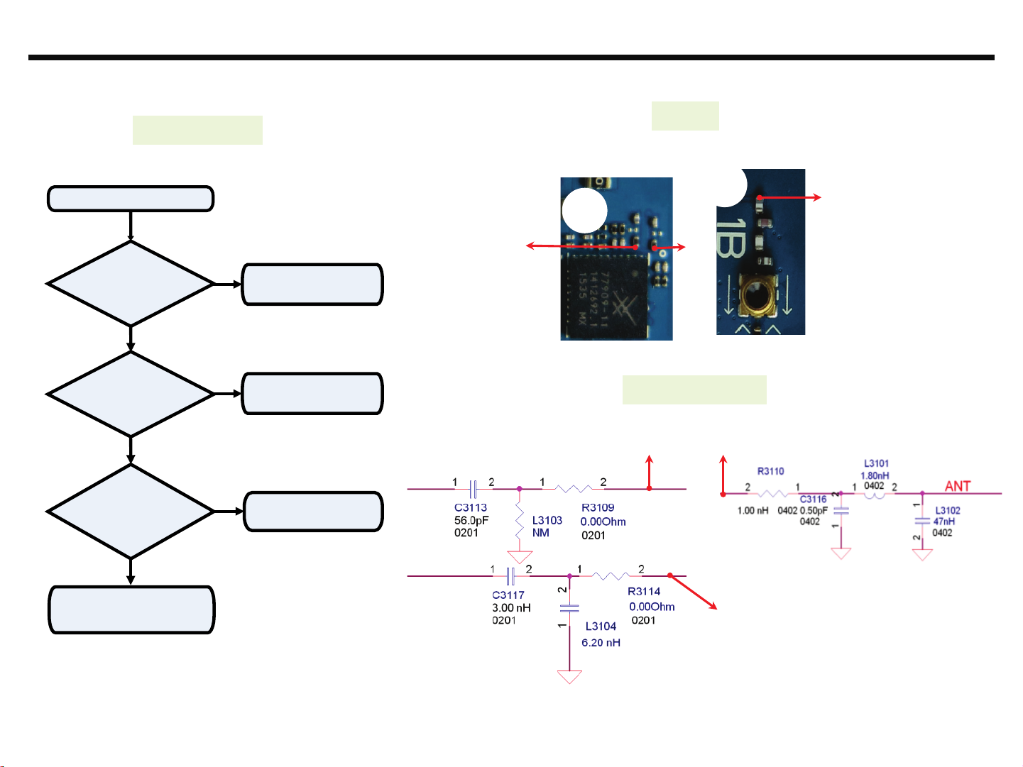
3.4 GSM RF PART
16
GSM RF Part support GSM850/900/1800/1900 with ASM, PAM, Transceiver component
Checking Flow
START
Check XO Block
Refer 3.1
Check Transceiver DC Power supply Block
Refer 3.2
Check FEM Block
Refer 3.3
3. TROUBLE SHOOTING
LGE Internal Use Only
Check T/RX Block
Re-Download & Cal
Change the Board
Copyright ⓒ 2016 LG Electronics. Inc. All right
reserved. Only training and service purposes
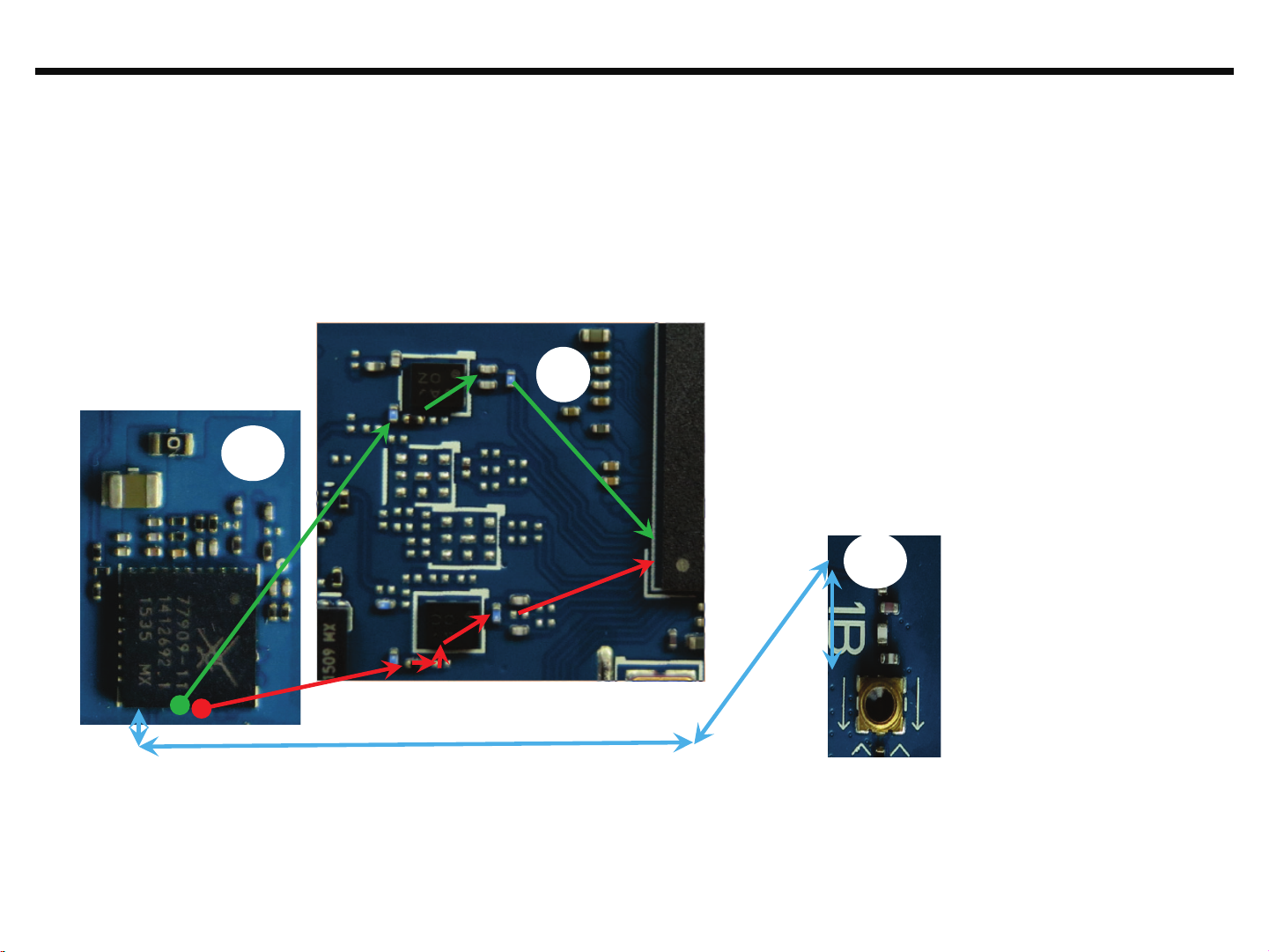
3.4 GSM RF PART
17
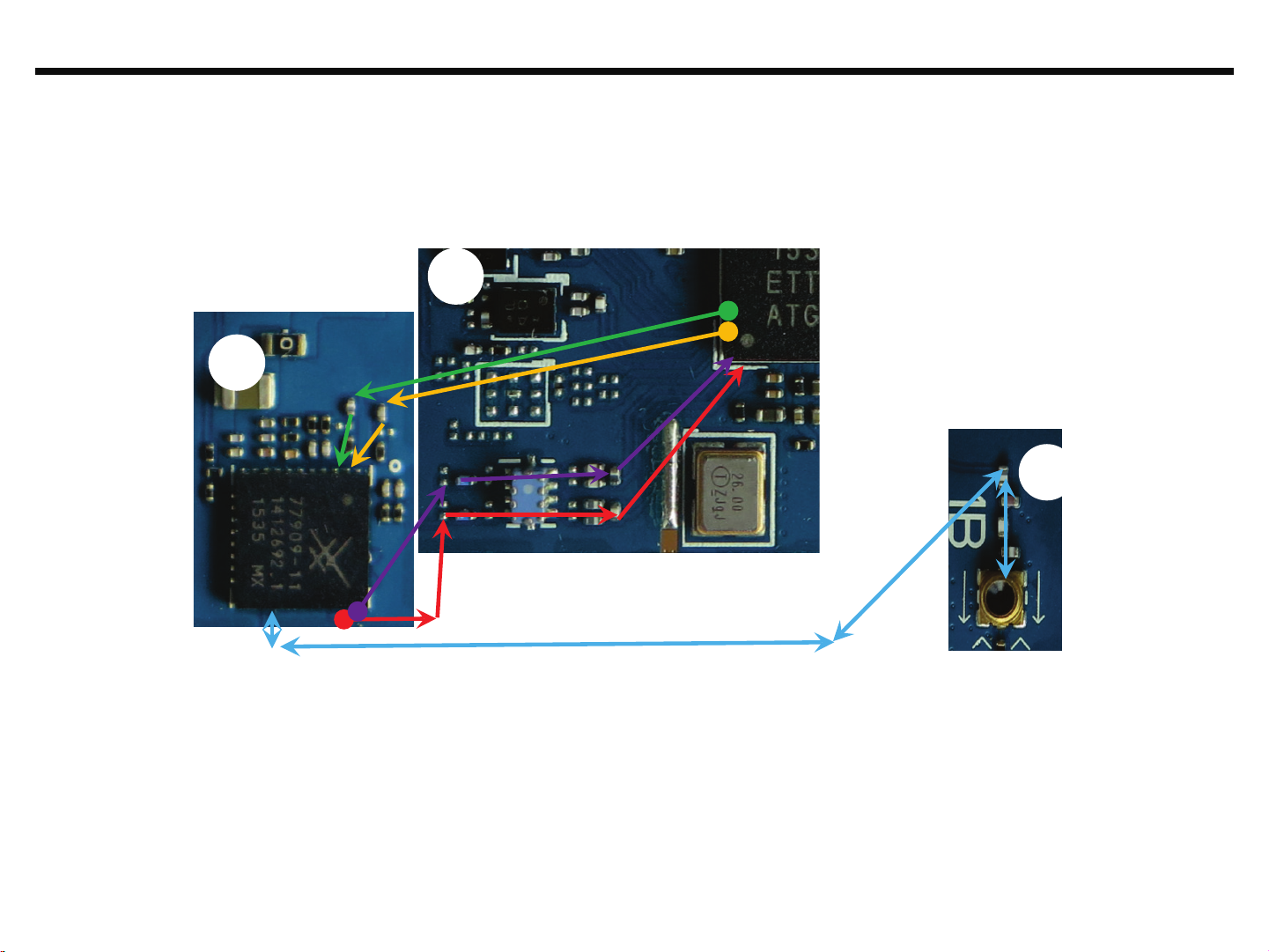
3.4.1 GSM850/900/1800/1900 Rx
Main
Bot
U3101
Main
Top
U1001
3. TROUBLE SHOOTING
GSM850/GSM900 RX PATH
1.
2.DCS1800/PCS1900 RX PATH
3.DCS1800/PCS1900 TX PATH
4.GSM850/GSM900 TX PATH
5.COMMON T/RX PATH
Main
Bot
LGE Internal Use Only
Image
J3101
Copyright ⓒ 2016 LG Electronics. Inc. All right
reserved. Only training and service purposes
3.4 GSM RF PART
18
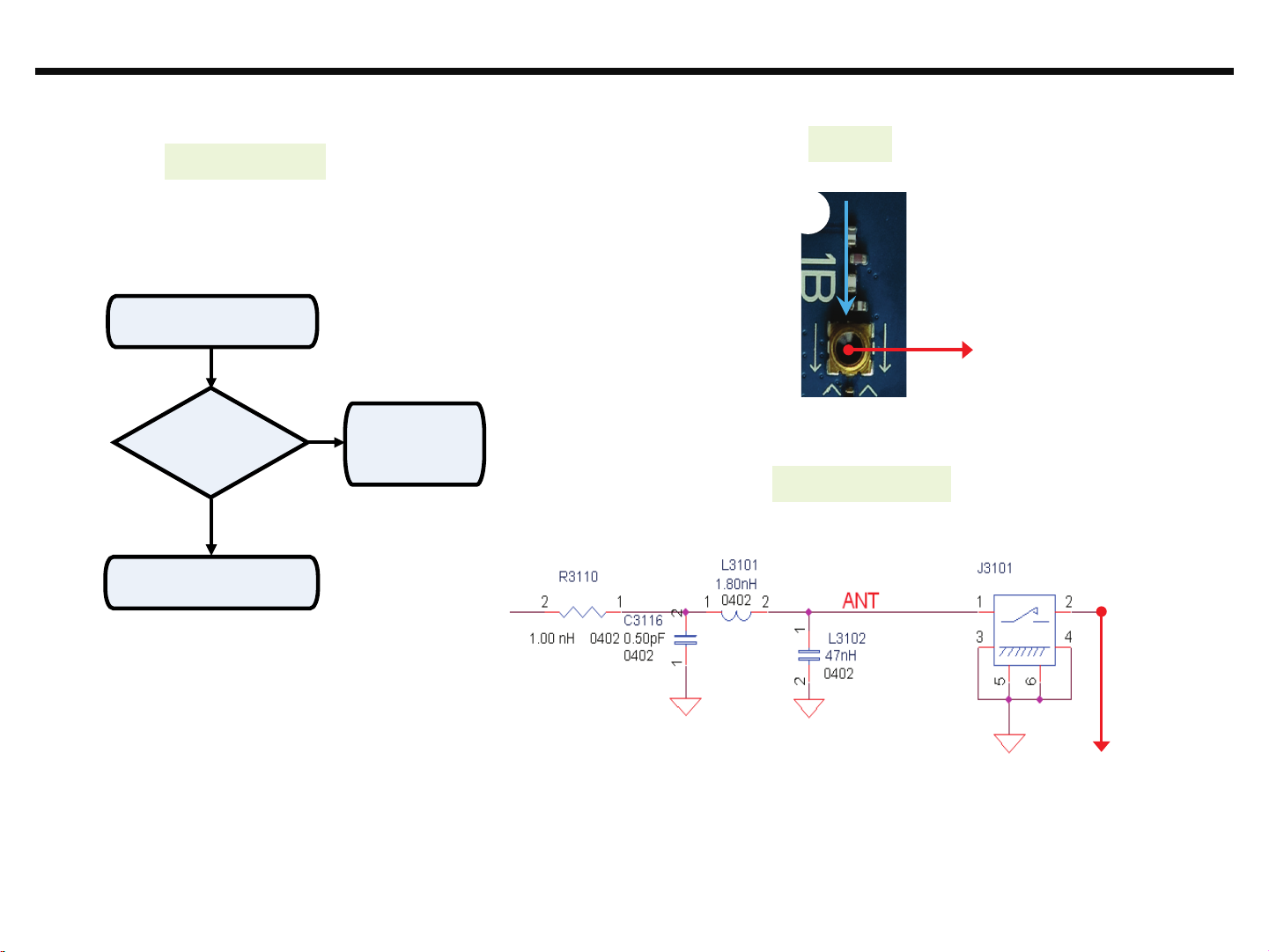
3.4.1.1 Checking RF signal path (SW)
Checking Flow
START
3. TROUBLE SHOOTING
Image
Main
Bot
TP1(J3101)
J3101
LGE Internal Use Only
Check
TP1
Signal exist?
YES
Check next step
NO
Check
J3101
Soldering
Circuit Diagram
TP1
Copyright ⓒ 2016 LG Electronics. Inc. All right
reserved. Only training and service purposes

3.4 GSM RF PART
19
3.4.1.2 Checking RF Signal RX path(GSM850/GSM900/DCS1800/PCS1900)
3. TROUBLE SHOOTING
Checking Flow
START
Check TP1/2 Signal exist?
YES
Check Transceiver
physical damage
or soldering condition
OK?
Check next step
NO
NOT GOOD
Check Component
above RF signal path
Replace U3101
Circuit Diagram
Main
Top
Image
SAW3101
TP1
TP2
TP1
LGE Internal Use Only
TP2
Copyright ⓒ 2016 LG Electronics. Inc. All right
reserved. Only training and service purposes
3.4 GSM RF PART
20
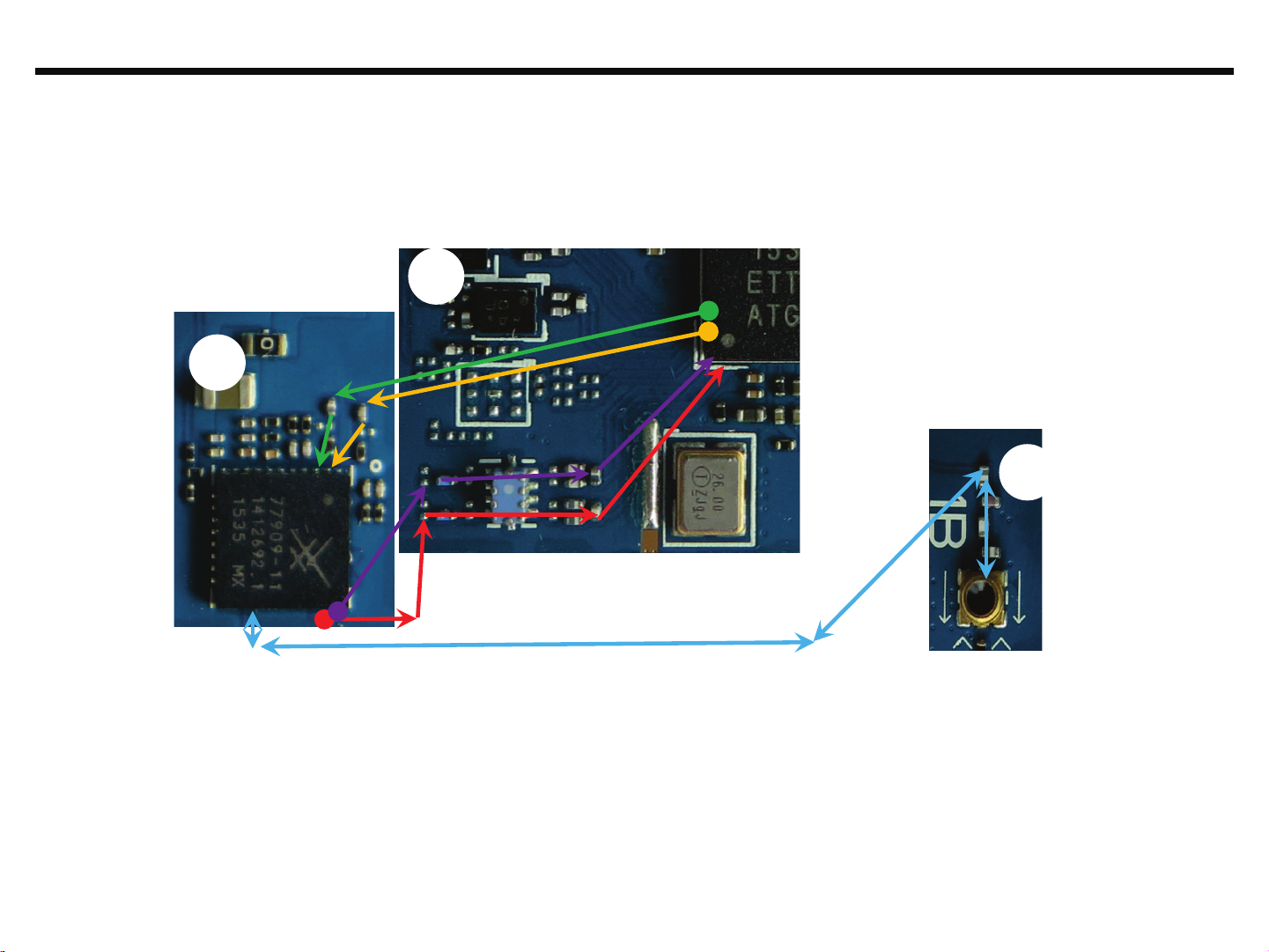
3.4.2.1 GSM850/900/1800/1900 Tx
Main
Bot
U3101
Main
Top
U1001
3. TROUBLE SHOOTING
GSM850/GSM900 RX PATH
1.
2.DCS1800/PCS1900 RX PATH
3.DCS1800/PCS1900 TX PATH
4.GSM850/GSM900 TX PATH
5.COMMON T/RX PATH
Main
Bot
LGE Internal Use Only
Image
J3101
Copyright ⓒ 2016 LG Electronics. Inc. All right
reserved. Only training and service purposes

3.4 GSM RF PART
21
3.4.2.2 Checking GSM PAM DC Power Circuit
Checking Flow
3. TROUBLE SHOOTING
Image
TP1
START
Check TP1 Supply voltage OK?
YES
Check FEM control logic OK?
Refer to 3.3 FEM Block.
Check TP2
If Vramp ok?
YES
Check Next step
The Problem may be Other
NO
The Problem may be Logic
NO
part
Check Logic part
part
TP2
U3101
Main
Bot
Circuit Diagram
TP2(0.1V~1.6V)R3102
TP1(3.4V~4.3V)R3105
LGE Internal Use Only
Copyright ⓒ 2016 LG Electronics. Inc. All right
reserved. Only training and service purposes

3.4 GSM RF PART
22
3.4.2.3 Checking RF signal path(SW)
Checking Flow
START
Check TP1
If DCS/PCS Over 30dBm?
If 850/900 Over 33dBm?
NO
YES
3. TROUBLE SHOOTING
Image
Main
Bot
TP1(J3101)
J3101
Check J3101 Soldering
Circuit Diagram
Check next step
LGE Internal Use Only
TP1
Copyright ⓒ 2016 LG Electronics. Inc. All right
reserved. Only training and service purposes
3.4 GSM RF PART
23
3.4.2.4 Checking RF signal path
Checking Flow
START
Main
Bot
3. TROUBLE SHOOTING
Image
Main
Bot
TP1
Check TP1
If GSM850/900 Over 32.5dBm?
If DCS/PCS Over 29.5dBm?
NO
Check TP2/3
If power at 0~6dBm?
NO
Check Transceiver physical damage
or soldering condition
OK?
Check next step
YES
YES
NOT GOOD
Check component
above RF signal path
Check U3101 soldering
Replace U1001
TP3
U3101
TP2
J3101
Circuit Diagram
TP2
TP1
TP3
LGE Internal Use Only
Copyright ⓒ 2016 LG Electronics. Inc. All right
reserved. Only training and service purposes
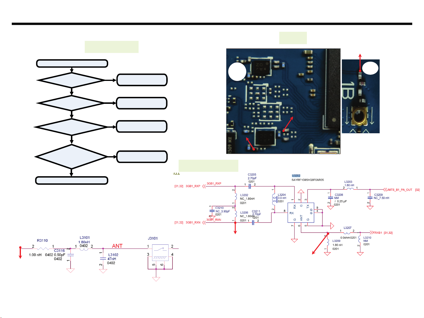
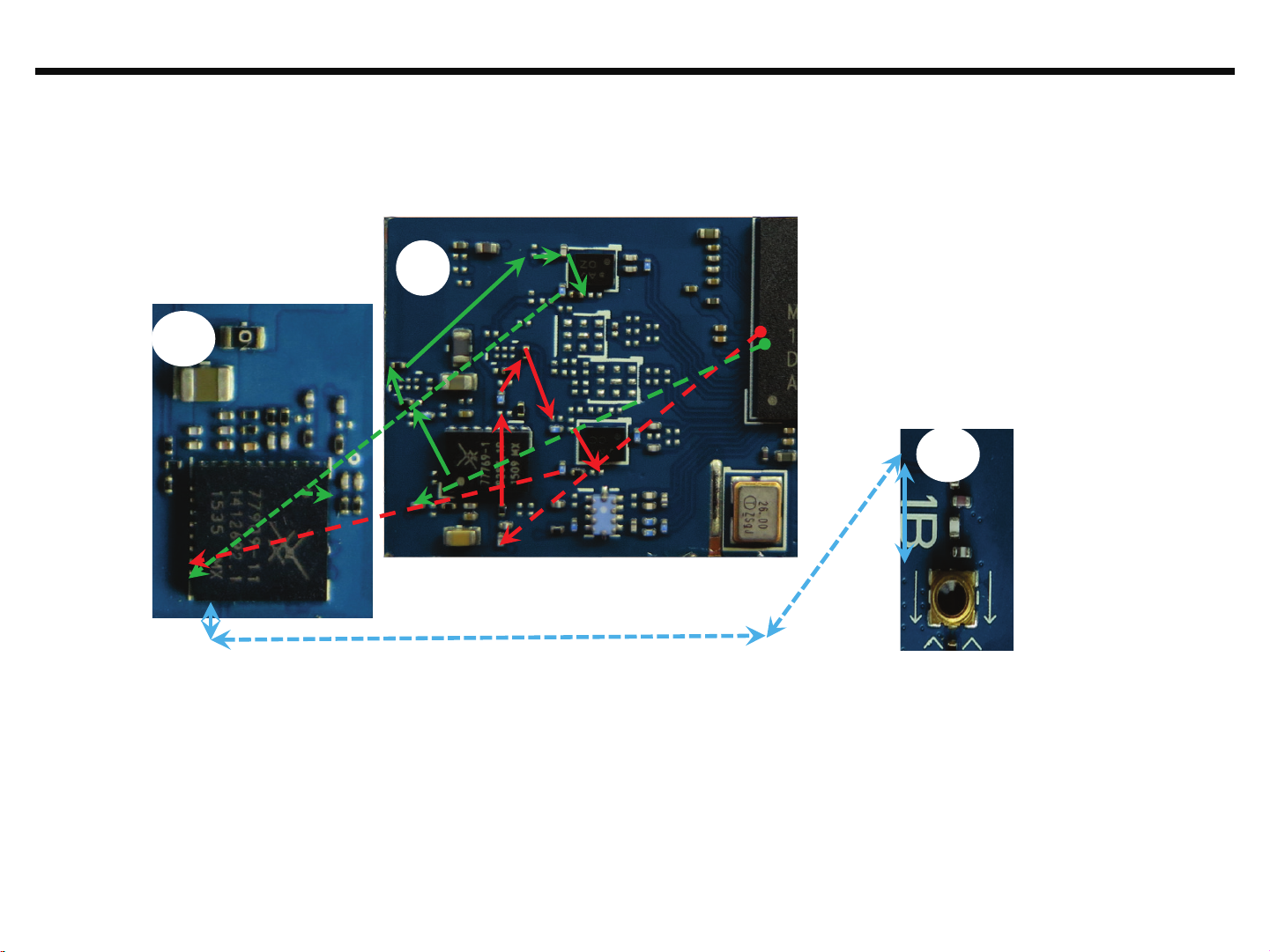
3.5 WCDMA RF Part
24
WCDMA RF Part support WCDMA B1/8 with FEM, PAM, Transceiver component
Checking Flow
START
Check XO Block
Refer 3.1
Check Transceiver DC Power supply Block
Refer 3.2
Check FEM Block
Refer 3.3
3. TROUBLE SHOOTING
LGE Internal Use Only
Check T/RX Block
Re-Download & Cal
Change the Board
Copyright ⓒ 2016 LG Electronics. Inc. All right
reserved. Only training and service purposes
3.5 WCDMA RF PART
25
3.5.1 WCDMA RF Part RX PATH (B1/B8)
1) WCDMA RX Path
Main
Bot
U3206
Image
Main
Top
3. TROUBLE SHOOTING
1.Band 1 RX PATH
2.Band 8 RX PATH
3.COMMON T/RX PATH
U1001
Main
Bot
U3101
LGE Internal Use Only
U3202
J3101
Copyright ⓒ 2016 LG Electronics. Inc. All right
reserved. Only training and service purposes
3.5 WCDMA RF PART
26
3. TROUBLE SHOOTING
3.5.1.1 Checking RF signal path(Band 1)
Checking Flow
START
Check TP1
Signal exist?
Check TP2
Signal exist?
YES
YES
Check TP3
Signal exist?
Transceiver physical damage
Check
YES
or soldering
condition
OK?
Check next step
NOT GOOD
Check J3101 Soldering
NO
Check U3101 Soldering
NO
Check U3202 Soldering
NO
Replace U1001
Circuit Diagram
Main
Top
TP2
U3206
U3202
Image
TP3
U1001
TP1
J3101
Main
Bot
TP1
LGE Internal Use Only
TP3
TP2
Copyright ⓒ 2016 LG Electronics. Inc. All right
reserved. Only training and service purposes

3.5 WCDMA RF PART
27
3.5.1.2 Checking RF signal path(Band 8)
Checking Flow
3. TROUBLE SHOOTING
Image
TP1
START
Check TP1
Signal exist?
YES
Check TP2
Signal exist?
YES
Check TP3
Signal exist?
YES
Transceiver physical damage
Check
or soldering
condition
OK?
Check next step
NO
NO
NO
NOT GOOD
Check J3101 Soldering
Check U3101 Soldering
Check U3206 Soldering
Replace U1001
U3206
U3202
Circuit Diagram
TP2
TP3
Main
Top
U1001
J3101
Main
Bot
TP1
LGE Internal Use Only
TP3
TP2
Copyright ⓒ 2016 LG Electronics. Inc. All right
reserved. Only training and service purposes
3.5 WCDMA RF PART
28
3.5.2 WCDMA RF Part TX PATH (B1/B8)
2) WCDMA TX Path
Main
Bot
Main
Top
Image
U3206
U1001
3. TROUBLE SHOOTING
1.Band 1 TX PATH
2.Band 8 TX PATH
3.COMMON T/RX PAT
H
LGE Internal Use Only
U3101
U3201
U3202
Main
Bot
J3101
Copyright ⓒ 2016 LG Electronics. Inc. All right
reserved. Only training and service purposes

3.5 WCDMA RF PART
29
3.5.2.1 Checking WCDMA PAM DC Power & Control Circuit
Checking Flow
START
3. TROUBLE SHOOTING
Image
TP1
Main
Top
Check TP1 Supply voltage OK?
YES
Check TP2 Supply voltage OK?
YES
Check TP3~5
If PAM control logic OK?
YES
Check Next step
The Problem may be Other
NO
NO
NO
Check Logic part
The Problem may be Other
Check Logic part
The Problem may be Other
Check Logic part
part
part
part
TP2(3.4V~4.3V)
TP1(3.4V~4.3V)
TP5
U3201
TP3
Circuit Diagram
TP4
TP2
TP3
TP4
TP5
LGE Internal Use Only
Copyright ⓒ 2016 LG Electronics. Inc. All right
reserved. Only training and service purposes
3.5 WCDMA RF PART
30
3.5.2.1 Checking WCDMA PAM DC Power & Control Circuit
U3201 PAM CONTROL LOGIC
3. TROUBLE SHOOTING
LGE Internal Use Only
Copyright ⓒ 2016 LG Electronics. Inc. All right
reserved. Only training and service purposes
 Loading...