

Page 1
SERVICE MANUAL MODEL : G5200 / W5200
GSM Phone
SERVICE MANUAL
P/N : MMBD0015801 JUNE, 2002
MODEL : G5200/W5200
Page 2

- 1 -
1. INTRODUCTION
.......................................
4
1.1 Purpose
..................................................
4
1.2 Regulatory Information
..........................
4
A. Security
..............................................
4
B. Incidence of Harm
..............................
4
C. Changes in Service
............................
4
D. Maintenance Limitations
....................
4
E. Notice of Radiated Emissions
.............
5
F. Pictures
..............................................
5
G. Interference and Attenuation
.............
5
H. Electrostatic Sensitive Devices
..........
5
1.3 Abbreviations
.........................................
6
2. PERFORMANCE
.....................................
8
2.1 H/W Feature
...........................................
8
2.2 Technical Specification
..........................
9
3. TECHNICAL BRIEF
............................
13
3.1 General Descreption
...........................
. 13
3.2 Receiver
...............................................
13
A. RF front end
.....................................
14
B. Demodulator and
baseband processing
......................
14
C. DC Offset Compensation
................
14
3.3 Transmitter Part
...................................
15
A. IF Modulator
...................................
. 15
B. OPLL
...............................................
16
C. Synthesizer
......................................
16
D. TX APC Part
....................................
17
E. Power Amplifier
................................
17
3.4 13 MHz Clock
......................................
18
3.5 Power Supplies and Control Signals
....
18
3.6 Digital Main Processor
.........................
19
3.7 Analog Main Processor
........................
24
3.8 Power Management
..............................
26
3.9 Memories
..............................................
28
3.10 Display and Interfaces
........................
28
3.11 Keypad Switches and Scanning
..........
29
3.12 Microphone
.........................................
30
3.13 Earpiece
.............................................
31
3.14 Hands-free Interface
..........................
32
3.15 Headset Jack Interface
.......................
32
3.16 Key Back-light Illumination
..................
32
3.17 LCD Back-light Illumination
................
33
3.18 Multi-Color LED Illumination
..............
33
3.19 Speaker & MIDI IC
.............................
34
4. TROUBLE SHOOTING
.....................
35
4.1 RF Components
.................................
35
4.2 Tx Trouble
..........................................
44
4.3 Power on Trouble
...............................
60
4.4 Charging Trouble
...............................
62
4.5 LCD Trouble
.......................................
64
4.6 Receiver Trouble .
...............................
66
4.7 Speaker Trouble
.................................
69
4.8 Mic Trouble
..........................................
72
4.9 Vibrator Trouble
.................................
75
4.10 Backlight Trouble
.............................
77
4.11 Folder on/off Trouble
........................
79
4.12 SIM Detect Trouble
..........................
81
4.13 Earphone Trouble
............................
83
4.14 HFK Trouble
.....................................
87
5. ASSEMBLY INSTRUCTION
............
95
5.1 Disassembly
.......................................
95
6. DOWNLOAD
.......................................
102
6.1 Download Setup
...............................
102
6.2 Download Procedure
........................
103
Table Of Contents
Page 3

- 2 -
7. BLOCK DIAGRAM
.............................
106
7.1 Main Board
.......................................
106
7.2 FPCB
................................................
107
7.3 RF
....................................................
107
8. CIRCUIT DIAGRAM
...........................
109
8.1 Baseband Interface
..........................
109
8.2 MIDI
..................................................
110
8.3 KYE, I/F & LCD CON
.......................
111
8.4 RF
....................................................
112
9. PCB LAYOUT
.....................................
113
10. ENGINEERING MODE
..................
115
10.1 BB Test [MENU 1]
........................
115
10.2 RF Test [MENU 2]
........................
117
10.3 MF Mode [MENU 3]
......................
118
10.4 Trace option [MENU 4]
.................
119
10.5 Call Timer [MENU 5]
.....................
119
10.6 Fact. Reset [MENU 6]
...................
119
10.7 S/W version [MENU 7]
..................
119
11. STAND ALONE TEST
...................
120
11.1 Introduction
...................................
120
11.2 Setting Method
.............................
120
11.3 Means of Test
...............................
120
12. AUTO CALIBRATION
...................
121
12.1 Overview
.......................................
121
12.2 Requirements
...............................
121
12.3 Menu and settings
........................
121
12.4 AGC
..............................................
123
12.5 APC
..............................................
123
12.6 ADC
..............................................
123
12.7 Setting
..........................................
123
12.8 How to do calibration
....................
123
13. EXPLODED VIEW &
REPLACEMENT PART LIST
......
124
13.1 Exploded View
..............................
124
13.2 Accessories
..................................
126
13.3 Replacement Part List
..................
127
Page 4

- 3 -
REVISED HISTORY
The information in this manual is subject to change without notice and should not be construed as
a commitment by LGE Inc. Furthermore, LGE Inc. reserves the right, without notice, to make
changes to equipment design as advances in engineering and manufacturing methods warrant.
This manual provides the information necessary to install, program, operate and maintain the
G5200.
DATE ISSUE CONTENTS OF CHANGES S/W VERSION
APRIL/2002 ISSUE 1 Initial Release
Page 5

1. INTRODUCTION
- 4 -
1. INTRODUCTION
1.1 Purpose
This manual provides the information necessary to repair, calibration, description and download the
features of the G5200.
1.2 Regulatory Information
A. Security
Toll fraud, the unauthorized use of telecommunications system by an unauthorized part
(for example, persons other than your company’s employees, agents, subcontractors, or person
working on your company’s behalf) can result in substantial additional charges for your
telecommunications services. System users are responsible for the security of own system.
There are may be risks of toll fraud associated with your telecommunications system. System users
are responsible for programming and configuring the equipment to prevent unauthorized use. LGE
does not warrant that this product is immune from the above case but will prevent unauthorized use
of common-carrier telecommunication service of facilities accessed through or connected to it. LGE
will not be responsible for any charges that result from such unauthorized use.
B. Incidence of Harm
If a telephone company determines that the equipment provided to customer is faulty and possibly
causing harm or interruption in service to the telephone network, it should disconnect telephone
service until repair can be done. A telephone company may temporarily disconnect service as long
as repair is not done.
C. Changes in Service
A local telephone company may make changes in its communications facilities or procedure. If
these changes could reasonably be expected to affect the use of the G5200 or compatibility with
the network, the telephone company is required to give advanced written notice to the user,
allowing the user to take appropriate steps to maintain telephone service.
D. Maintenance Limitations
Maintenance limitations on the G5200 must be performed only by the LGE or its authorized agent.
The user may not make any changes and/or repairs expect as specifically noted in this manual.
Therefore, note that unauthorized alternations or repair may affect the regulatory status of the
system and may void any remaining warranty.
Page 6
1. INTRODUCTION
- 5 -
E. Notice of Radiated Emissions
The G5200 complies with rules regarding radiation and radio frequency emission as defined by
local regulatory agencies. In accordance with these agencies, you may be required to provide
information such as the following to the end user.
F. Pictures
The pictures in this manual are for illustrative purposes only; your actual hardware may look slightly
different.
G. Interference and Attenuation
An G5200 may interfere with sensitive laboratory equipment, medical equipment, etc.
Interference from unsuppressed engines or electric motors may cause problems.
H. Electrostatic Sensitive Devices
ATTENTION
Boards, which contain Electrostatic Sensitive Device (ESD), are indicated by the sign.
Following information is ESD handling:
Service personnel should ground themselves by using a wrist strap when exchange system
boards.
When repairs are made to a system board, they should spread the floor with anti-static mat which
is also grounded.
Use a suitable, grounded soldering iron.
Keep sensitive parts in these protective packages until these are used.
When returning system boards or parts like EEPROM to the factory, use the protective package
as described.
Page 7
1. INTRODUCTION
- 6 -
1.3 Abbreviations
For the purposes of this manual, following abbreviations apply:
APC Automatic Power Control
BB Baseband
BER Bit Error Ratio
CC-CV Constant Current – Constant Voltage
DAC Digital to Analog Converter
DCS Digital Communication System
dBm dB relative to 1 milliwatt
DSP Digital Signal Processing
EEPROM Electrical Erasable Programmable Read-Only Memory
EL Electroluminescence
ESD Electrostatic Discharge
FPCB Flexible Printed Circuit Board
GMSK Gaussian Minimum Shift Keying
GPIB General Purpose Interface Bus
GPRS General Packet Radio Service
GSM Global System for Mobile Communications
IPUI International Portable User Identity
IF Intermediate Frequency
LCD Liquid Crystal Display
LDO Low Drop Output
LED Light Emitting Diodet
G5200 LG GSM Phone
LGE LG Electronics
OPLL Offset Phase Locked Loop
PAM Power Amplifier Module
PCB Printed Circuit Board
PGA Programmable Gain Amplifier
PLL Phase Locked Loopr
PSTN Public Switched Telephone Network
RF Radio Frequency
RLR Receiving Loudness Rating
RMS Root Mean Square
RTC Real Time Clock
SAW Surface Acoustic Wave
SIM Subscriber Identity Module
SLR Sending Loudness Rating
SRAM Static Random Access Memory
STMR Side Tone Masking Rating
TA Travel Adapter
Page 8
1. INTRODUCTION
- 7 -
TDD Time Division Duplex
TDMA Time Division Multiple Access
UART Universal Asynchronous Receiver/Transmitter
VCO Voltage Controlled Oscillator
VCTCXO Voltage Control Temperature Compensated Crystal Oscillator
WAP Wireless Application Protocol
Page 9
2. PERFORMANCE
- 8 -
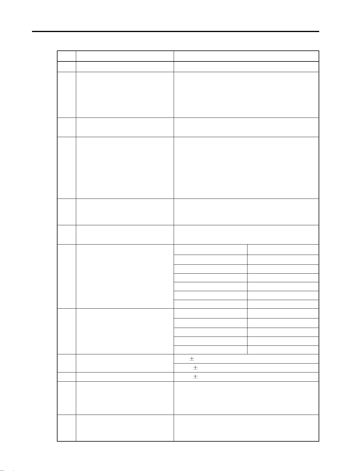
2. PERFORMANCE
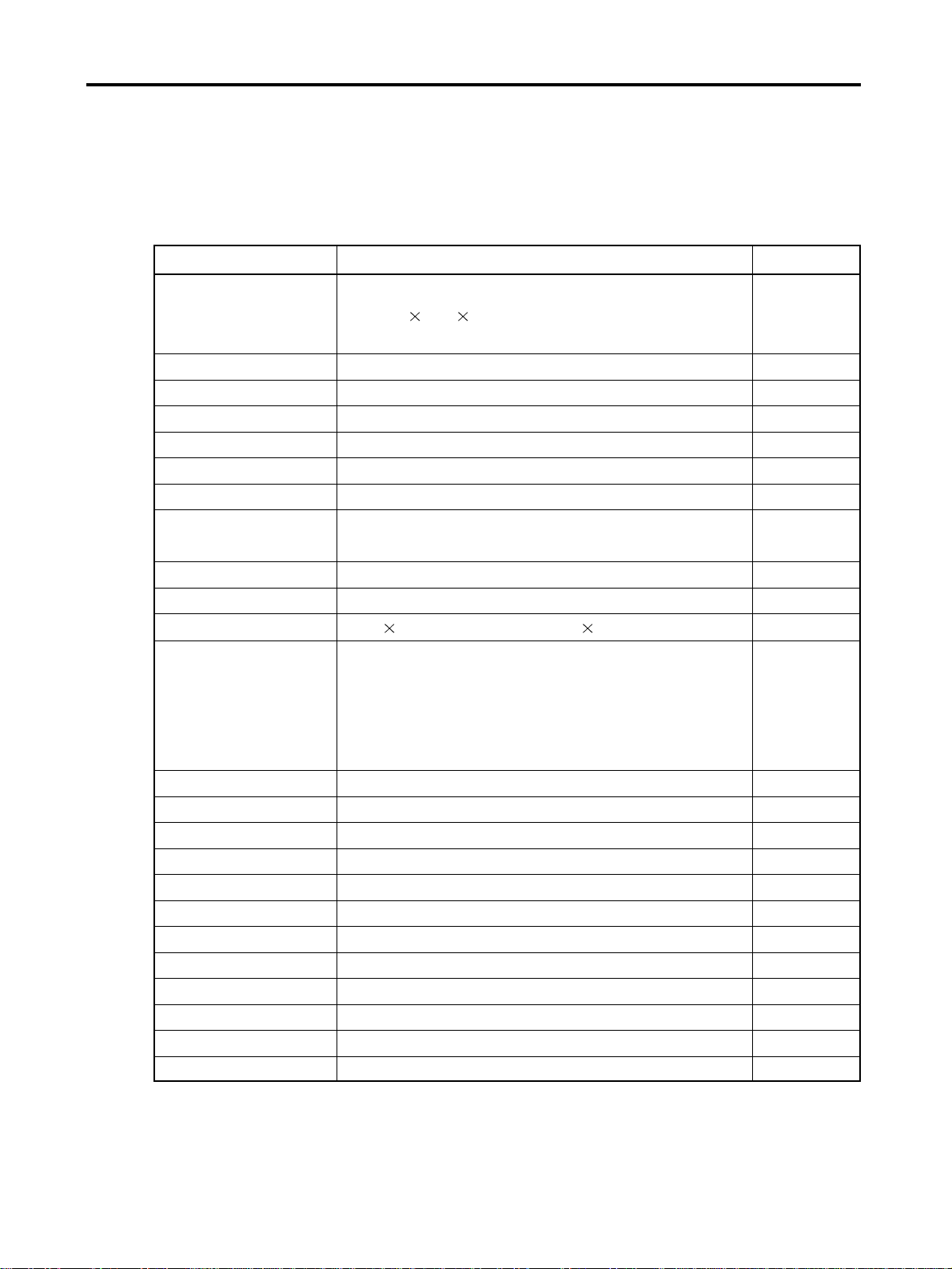
2.1 H/W Features
Item Feature Comment
Li-ion, 750 mAh
Standard Battery Size: 41 73.9 5mm
Weight: 22 g
AVG TCVR Current GSM , EGSM: 243 mA, DCS: 209 mA
Stand by Current < 4 mA
Talk time Up to 3 hours (GSM TX Level 7)
Stand by time Up to 200 hours (Paging Period: 9, RSSI: -85 dBm)
Charging time 2 hours 30mins
RX Sensitivity GSM, EGSM: -108 dBm, DCS: -107 dBm
TX output power GSM, EGSM: 32 dBm (Level 5)
DCS: 29.5 dBm (Level 0)
GPRS compatibility Class 10 (This only applies to G5200)
SIM card type 3V Small
Display 128 128 dots LCD(Main) , 96 64 dotsLCD(Sub)
Soft icons
Key Pad
Status Indicator 0 ~ 9, #, *, Navigation Key, Up/Down Side Key
Side Key, Confirm Key, Clear Key , Hot Key)
Send Key, END/PWR Key
ANT External
EAR Phone Jack Yes
PC Synchronization Yes
Speech coding EFR/FR/HR
Data and Fax Yes
Vibrator Yes
Receiver Yes
Roud Speaker Yes
Voice Recoding Yes
C-Mike Yes
Travel Adapter Yes
Options Hands-free kit, CLA, Data Kit
Page 10
2. PERFORMANCE
- 9 -
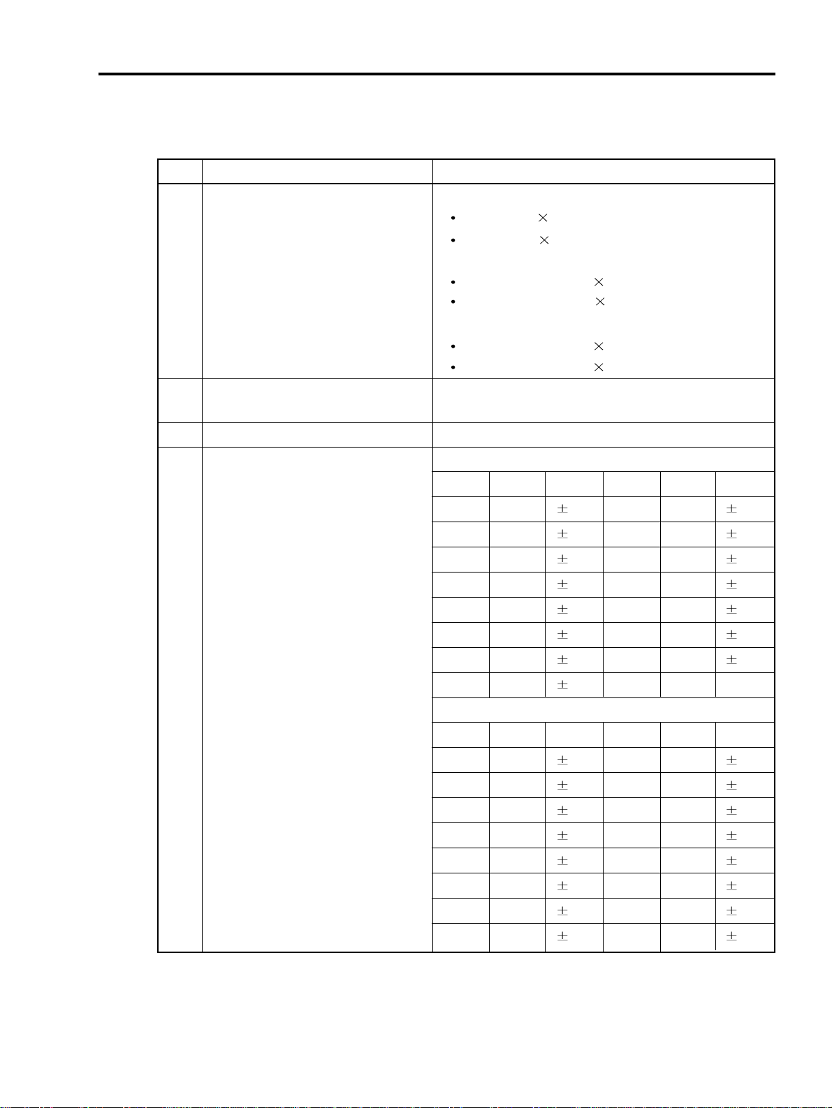
2.2 Technical Specification
Item Description Specification
GSM
TX: 890 + n 0.2 MHz
RX: 935 + n 0.2 MHz (n = 1 ~ 124)
EGSM
1 Frequency Band TX: 890 + (n – 1024) 0.2 MHz
RX: 935 + (n – 1024) 0.2 MHz (n = 975 ~ 1024)
DCS
TX: 1710 + (n – 512) 0.2 MHz
Rx: 1805 + (n – 512) 0.2 MHz (n = 512 ~ 885)
2 Phase Error
RMS < 5 degrees
Peak < 20 degrees
3 Frequency Error < 0.1 ppm
GSM, EGSM
Level Power Toler. Level Power Toler.
5 33 dBm 2dB 13 17 dBm 3dB
6 31 dBm 3dB 14 15 dBm 3dB
7 29 dBm 3dB 15 13 dBm 3dB
8 27 dBm 3dB 16 11 dBm 5dB
9 25 dBm 3dB 17 9 dBm 5dB
10 23 dBm 3dB 18 7 dBm 5dB
11 21 dBm 3dB 19 5 dBm 5dB
4 Power Level 12 19 dBm 3dB
DCS
Level Power Toler. Level Power Toler.
0 30 dBm 2dB 8 14 dBm 3dB
1 28 dBm 3dB 9 12 dBm 4dB
2 26 dBm 3dB 10 10 dBm 4dB
3 24 dBm 3dB 11 8 dBm 4dB
4 22 dBm 3dB 12 6 dBm 4dB
5 20 dBm 3dB 13 4 dBm 4dB
6 18 dBm 3dB 14 2 dBm 5dB
7 16 dBm
3dB 15 0 dBm 5dB
Page 11
2. PERFORMANCE
- 10 -
Item Description Specification
GSM, EGSM
Offset from Carrier (kHz). Max. dBc
100 +0.5
200 -30
250 -33
400 -60
600 ~ 1,200 -60
1,200 ~ 1,800 -60
1,800 ~ 3,000 -63
3,000 ~ 6,000 -65
5 Output RF Spectrum 6,000 -71
(due to modulation)
DCS
Offset from Carrier (kHz). Max. dBc
100 +0.5
200 -30
250 -33
400 -60
600 ~ 1,200 -60
1,200 ~ 1,800 -60
1,800 ~ 3,000 -65
3,000 ~ 6,000 -65
6,000 -73
GSM, EGSM
Offset from Carrier (kHz) Max. (dBm)
400 -19
600 -21
1,200 -21
6 Output RF Spectrum 1,800 -24
(due to switching transient)
GSM
Offset from Carrier (kHz) Max. (dBm)
400 -22
600 -24
1,200 -24
1,800 -27
7 Spurious Emissions Conduction, Emission Status
Page 12
2. PERFORMANCE
- 11 -
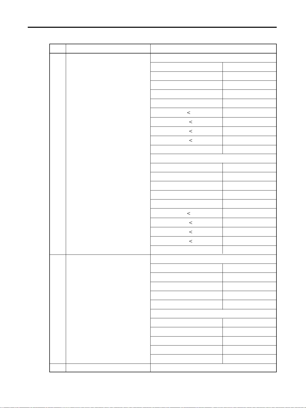
Item Description Specification
GSM, EGSM
8 Bit Error Ratio
BER (Class II) < 2.439% @-102 dBm
DCS
BER (Class II) < 2.439% @-100 dBm
9 RX Level Report Accuracy 3 dB
10 SLR 8 3 dB
Frequency (Hz) Max.(dB) Min.(dB)
100 -12 200 0 300 0 -12
11 Sending Response 1,000 0 -6
2,000 4 -6
3,000 4 -6
3,400 4 -9
4,000 0 -
12 RLR 2 3 dB
Frequency (Hz) Max.(dB) Min.(dB)
100 -12 200 0 300 2 -7
500
*
-5
13 Receiving Response 1,000 0 -5
3,000 2 -5
3,400 2 -10
4,000 2
* Mean that Adopt a straight line in between 300 Hz
and 1,000 Hz to be Max. level in the range.
14 STMR 13 5 dB
15 Stability Margin > 6 dB
dB to ARL (dB) Level Ratio (dB)
-35 17.5
-30 22.5
16 Distortion
-20 30.7
-10 33.3
0 33.7
7 31.7
10 25.5
17 Side Tone Distortion Three stage distortion < 10%
18
System frequency (13 MHz) tolerance
≤ 2.5 ppm
Page 13
2. PERFORMANCE
- 12 -
Item Description Specification
19 32.768KHz tolerance ≤ 30 ppm
Full power
< 243 mA (GSM, EGSM) ; < 209 mA (DCS)
20 Power Consumption
Standby
- Normal < 4 mA (Max. power)
21 Talk Time
GSM/ Level 7 (Battery Capacity 750mA): Up to 180
Min
GSM/ Level 12 (Battery Capacity 750mA): Up to 300 Min
Under conditions, Up to 200 hours:
1. Brand new and full 750mAh battery
2. Full charge, no receive/send and keep GSM in idle
22 Standby Time mode.
3. Broadcast set off.
4. Signal strength display set at 3 level above.
5. Backlight of phone set off.
At least 80 dB under below conditions:
23 Ringer Volume 1. Ringer set as ringer.
2. Test distance set as 50 cm
24 Charge Voltage
Fast Charge : < 500 mA
Slow Charge: < 60 mA
Antenna Bar Number Power
5 -85 dBm ~
4 -90 dBm ~ -86 dBm
25 Antenna Display 3 -95 dBm ~ -91 dBm
2 -100 dBm ~ -96 dBm
1 -105 dBm ~ -101 dBm
0 ~ -105 dBm
Battery Bar Number Voltage
0 ~ 3.62 V
26 Battery Indicator 1 3.62 ~ 3.73 V
2 3.73 ~ 3.82 V
3 3.82 V ~
27 Low Voltage Warning
3.5 0.03 V (Call)
3.62 0.03 V (Standby)
28 Forced shut down Voltage 3.35 0.03 V
1 Li-ion Battery
29 Battery Type
Standard Voltage = 3.7 V
Battery full charge voltage = 4.2 V
Capacity: 750 mAh
Switching-mode charger
30 Travel Charger Input: 100 ~ 240 V, 50/60 Hz
Output: 5.2 V, 600 mA
Page 14
3. TECHNICAL BRIEF
- 13 -
3. TECHNICAL BRIEF
3.1 General Descreption
The RF parts consists of a transmitter part,a receiver part,a synthesizer part,a voltage supply part,a
VCTCXO part. And the main RF Chipset CX74017[U411]is a single-chip dual-band transceiver for
the extended global system for mobile communication[E- GSM900MHz]/Digital communication
system[DCS1800MHz] voice and data transfer applications.
This device integrated a direct conversion receiver architecture, which eliminates the need of
Intermediate Frequency, a transmitter based on a modulation loop architecture and fractional-N
synthesizer part with built in TXVCO and Local-VCO.
3.2 Receiver
The Receiver part in CX74017 contains all active circuits completely, full receiver chain with the
exception of discrete front-end RF SAW filters. The filtered and amplified signal is down converted
in the RF-mixer to the baseband output. The receiver path is supported by internal channel filtering.
The RF front-end circuit is shown Figure 3-1.
Figure 3-1. RF front-end circuit.
Page 15
3. TECHNICAL BRIEF
- 14 -
A. RF front end
RF front end consists of Antenna Switch(U405), dual band LNAs integrated in transceiver(U411).
The Received RF signals (GSM 925MHz ~ 960MHz, DCS 1805MHz ~ 1880MHz) are fed into the
antenna or mobile switch. An antenna matching circuit is between the antenna and the mobile
switch.
The Antenna Switch (U405) is used to control the Rx and TX paths. And, the input signals VC1 and
VC2 of a U405 are connected to 2-Input AND Gates(U401) to switch either TX or RX path on.
When the RX path is turned on, the received RF signal then feeds either Rx_900_RF or
RX_1800_RF path selected by GSM-RX and DCS-RX respectively. This Rx_900_RF path contains
one SAW filter, followed after the Antenna Switch (U405), to filter any unwanted signal apart from
the DCS RX band. And, the RX_1800_RF path is the same case.
The logic and current for Antenna Switch is given below Table 3-1.
Table 3-1. The logic and current
These two paths are then connected to the LNAGSMN (#11) and LNADCSIN (#13) of CX74017
(U411), respectively. A low-noise bipolar RF amplifier, contained within the U411, amplifies the RF
signal. The RF signals from the front-end pass to the receiver mixers within the U411 device.
B. Demodulator and baseband processing
In direct conversion receiver there is only one mixer down-converting received RF signal to BB
signal directly. The gain down converting mixer is 40dB at high gain mode and 22dB at low gain
mode.
The Rx gain setting is done in the AGC algorithm. The nominal gain of the receiver is set as a
function of the expected signal strength at the antenna input so that a desired level is reached at
the Rx I/Q. 7 blocks in the receiver chain have variable gains, LNA, Mixer, LPF1, VGA1, gmC Filter,
Auxiliary gain control and VGA2. The gain settings can be adjustable via 3-wire bus control lines.
The baseband signals pass via integrated low-pass filters to the baseband A/D converters.
The remainder of the channel filtering is performed by the baseband chipset. The demodulator
contains switches to maintain the sense of the baseband I/Q outputs with respect to the incoming
RF signal on both GSM900 and DCS 1800.
C. DC Offset Compensation
Three correction loops ensure that DC offsets, generated in the CX74017, do not overload the
baseband chain at any point.
After compensation, the correction voltages are held on capacitors for the duration of the receive
slot(s). A rising edge on the RXEN signal, selected via the serial interface, placed the DC
compensation circuitry in the track mode.
VC1 VC2 Current
GSM TX 0 V 2.7 V 10.0 mA max
DCS TX 2.7 V 0 V 10.0 mA max
GSM/DCS RX 0 V 0 V < 0.1 mA
Page 16
3. TECHNICAL BRIEF
- 15 -
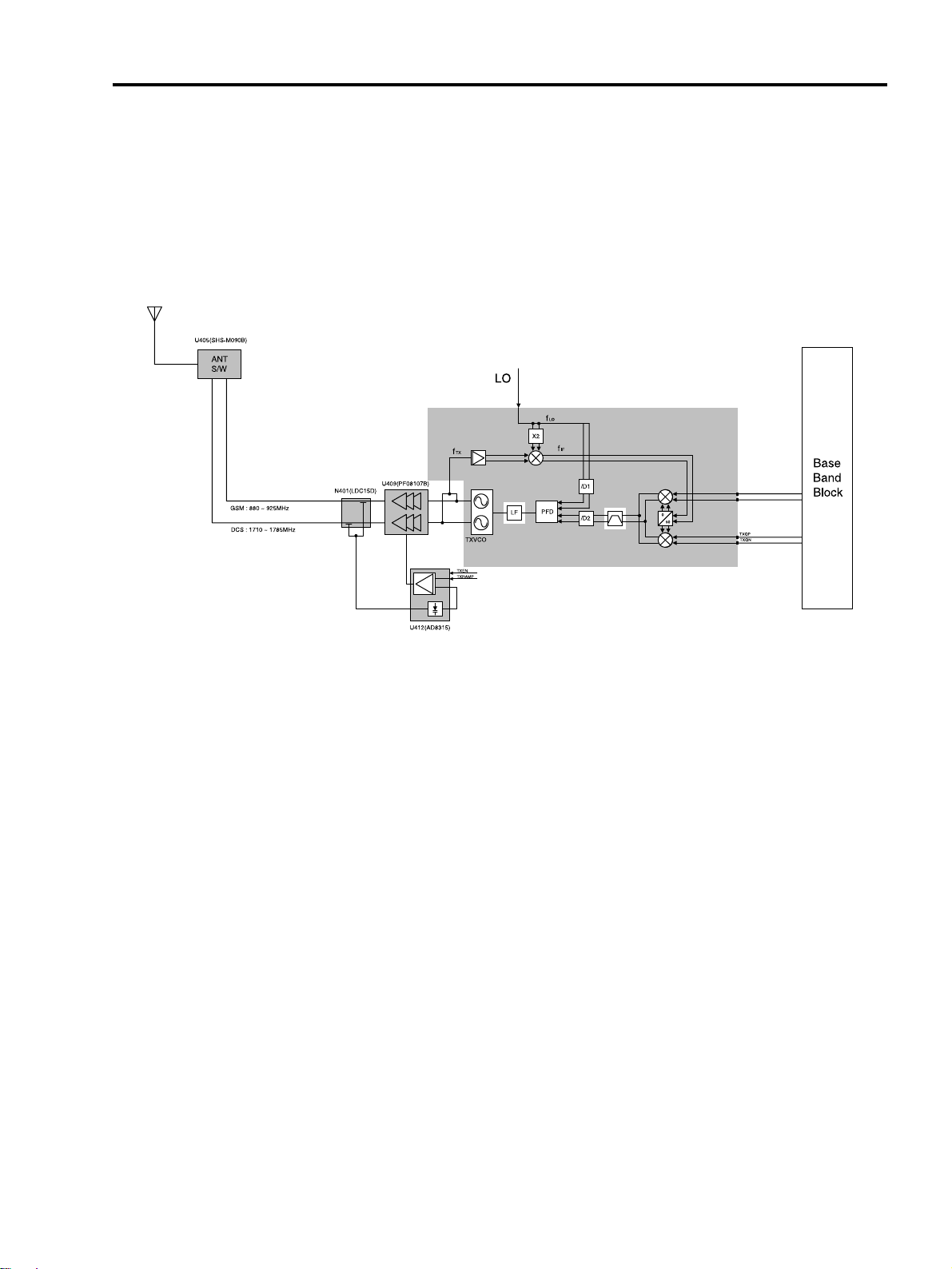
3.3 Transmitter Part
The Transmitter part contains CX74017 active parts and PAM, APC IC, coupler and Antenna
Switch. The CX74017 active part consists of a vector modulator and offset phase-locked loop
block(OPLL) including down-converter, phase detector, loop filter and dual band transmit VCO
which can operate at either final RF output frequency. The RF GMSK outputs from the transmit
VCO are fed directly to the RF power amplifiers.
Figure 3-2. Transmitter Block diagram
The peak output power and the profile of the transmitted burst are controlled by means of a closed
feedback loop. A dual band directional coupler is used to sample the RF output from either PA.
The PA outputs from the directional coupler pass to the antenna connector via Antenna Switch.
A. IF Modulator
The baseband converter(BBC) within the GSM chipset generates I and Q baseband signals for the
transmit vector modulator. The modulator provides more than 40dBc of carrier and unwanted sideband rejection and produces a GMSK modulated signal. The baseband software is able to cancel
out differential DC offsets in the I/Q baseband signals caused by imperfections in the D/A
converters.
The TX-Modulator implements a quadrature modulator. The IF-frequency input signal is split into
two precise orthogonal carriers, which are multiplied by the baseband modulation signal IT/ITX and
QT/QTX. It is used as reference signal for the OPLL.
TXIP
TXIN
Page 17
B. OPLL
The offset mixer down converts the feedback Tx RF signal using LO to generate a IF modulating
signal. The IF signal goes via external passive bandpass filter to one port of the phase detector.
The other side of the phase detector input is LO signal. The phase detector generates an error
current proportional to the phase difference between the modulated signal from the offset mixer and
the reference signal from the LO.
The error current is filtered by a second order low-pass filter to generate an output voltage which
depends on the GMSK modulation and the desired channel frequency. This voltage controls the
transmit VCO such that the VCO output signal, centered on the correct RF channel, is frequency
modulated with the original GMSK data. The OPLL acts as a tracking narrowband band pass filter
tuned to the desired channel frequency. This reduces the wideband noise floor of the modulation
and up-conversion process and provides significant filtering of spurious products.
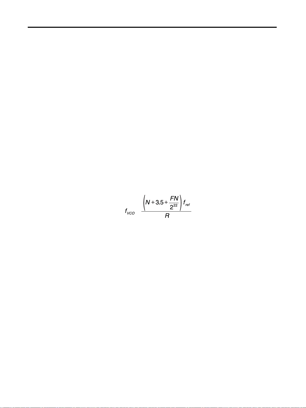
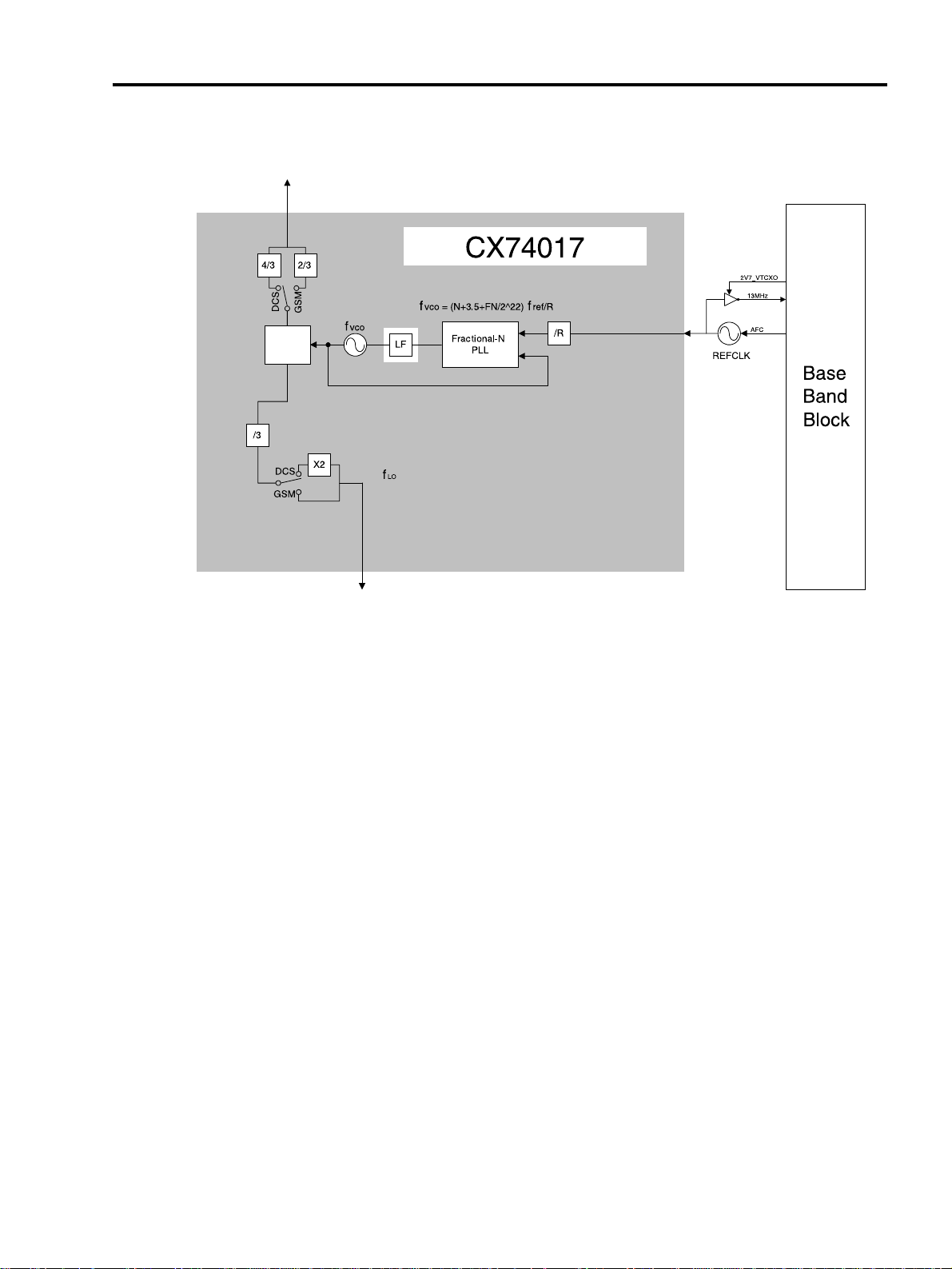
C. Synthesizer
The CX74017 includes a fully integrated UHF VCO with an on-chip LC tank.
A single sigma-delta fractional-N synthesizer can phase lock the local osillator used in both transmit
and receive path to a precision frequency reference input. Fractional-N operation offers low phase
noise and fast setting times, allowing for multiple slot applications such as GPRS.
The generated frequency is given by the following equation
where : = Generated VCO frequency
N = N-divider ratio integer part
FN = Fractional setting
R = R-divider ratio
= Reference Frequency
3. TECHNICAL BRIEF
- 16 -
=
VCOfVCO
f
Page 18
3. TECHNICAL BRIEF
- 17 -
The counter and mode settings of the synthesizer are also programmed via 3-wire interface.
Figure 3-3. Synthesizer Block diagram
D. TX APC Part
The AD8315[U412] is a dual band RF power controller for RF power amplifiers operating in the
850MHz to 2GHz range.
The AD8315[U412] controls the power output of the selected RF channel. RF power is controlled by
driving the RF amplifier power control pins and sensing the resultant RF output power via a
directional coupler. The RF sense voltage is peak detected using an on-chip Schottky diode.
This detected voltage is compared to the DAC voltage at the VSET pin to control the output power.
An internal input signal[TXRAMP] is applied to the positive input of the AD8315 amplifier during the
TXEN mode and a directional coupler near the antenna feeds a portion of the RF output signal back
to the AD8315 peak detector converts this signal to a low frequency feedback signal that balances
the amplifier when this signal equals the RAMP input signal level.
E. Power Amplifier
The PF08107B[U409] is Dual band amplifier for E-GSM(880 to 915MHz) and DCS1800(1710 to
1785MHz). The efficiency of module is the 50% at nominal output power for E-GSM and the 43% at
32dBm for DCS1800. This module should be operated under the GSM burst pulse. To avoid
permanent degradation, CW operation should not be applied. To avoid the oscillation at no input
power, before the input is cut off, the control voltage Vapc should be control to less than 0.5V.
We have to improve thermal resistance, the through holes should be layouted as many as possible
on PCB under the module. And to get good stability, all the GND terminals and the metal cap should
be soldered to ground plane of PCB.
13MHz
f
ref
Page 19
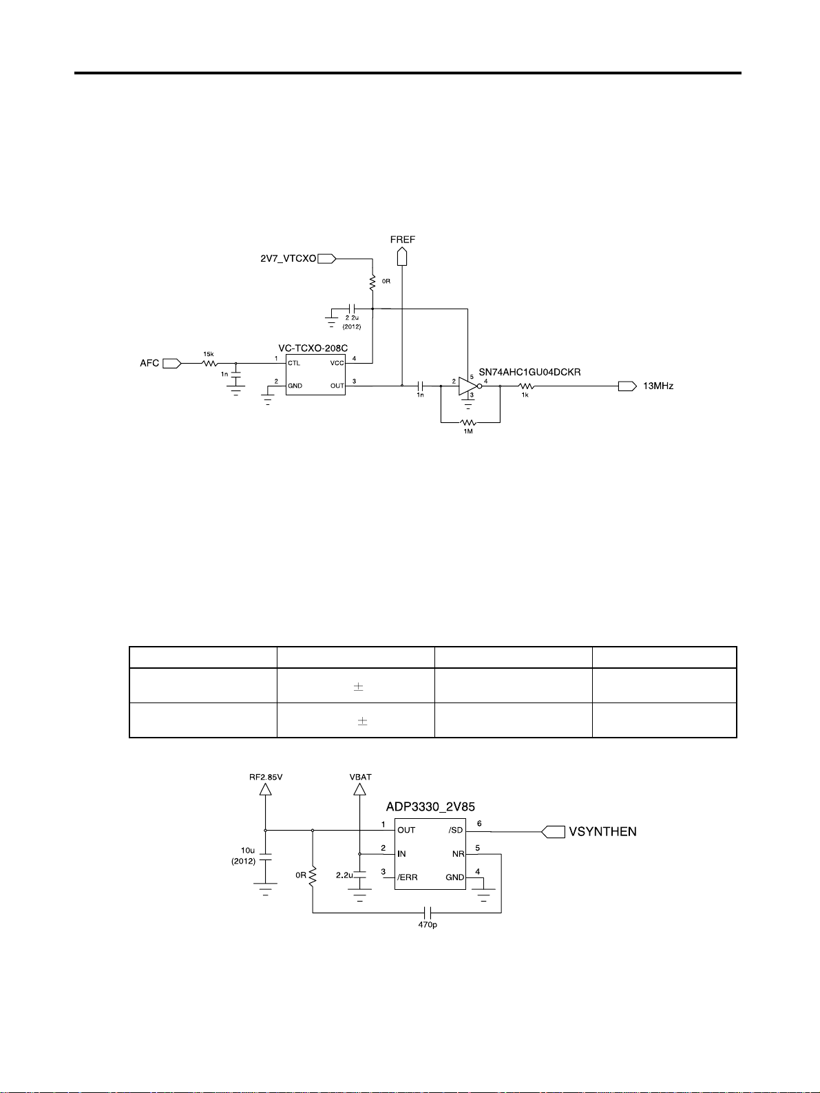
3.4 13 MHz Clock
The 13 MHz clock (VC-TCXO-208C) consists of a TCXO (Temperature Compensated Crystal
Oscillator) which oscillates at a frequency of 13 MHz.
It is used within the CX74017 RF Main Chip, BB Analog chip-set (AD6521), and Digital (AD6522).
Figure 3-4. VCTCXO Circuit.
3.5 Power Supplies and Control Signals
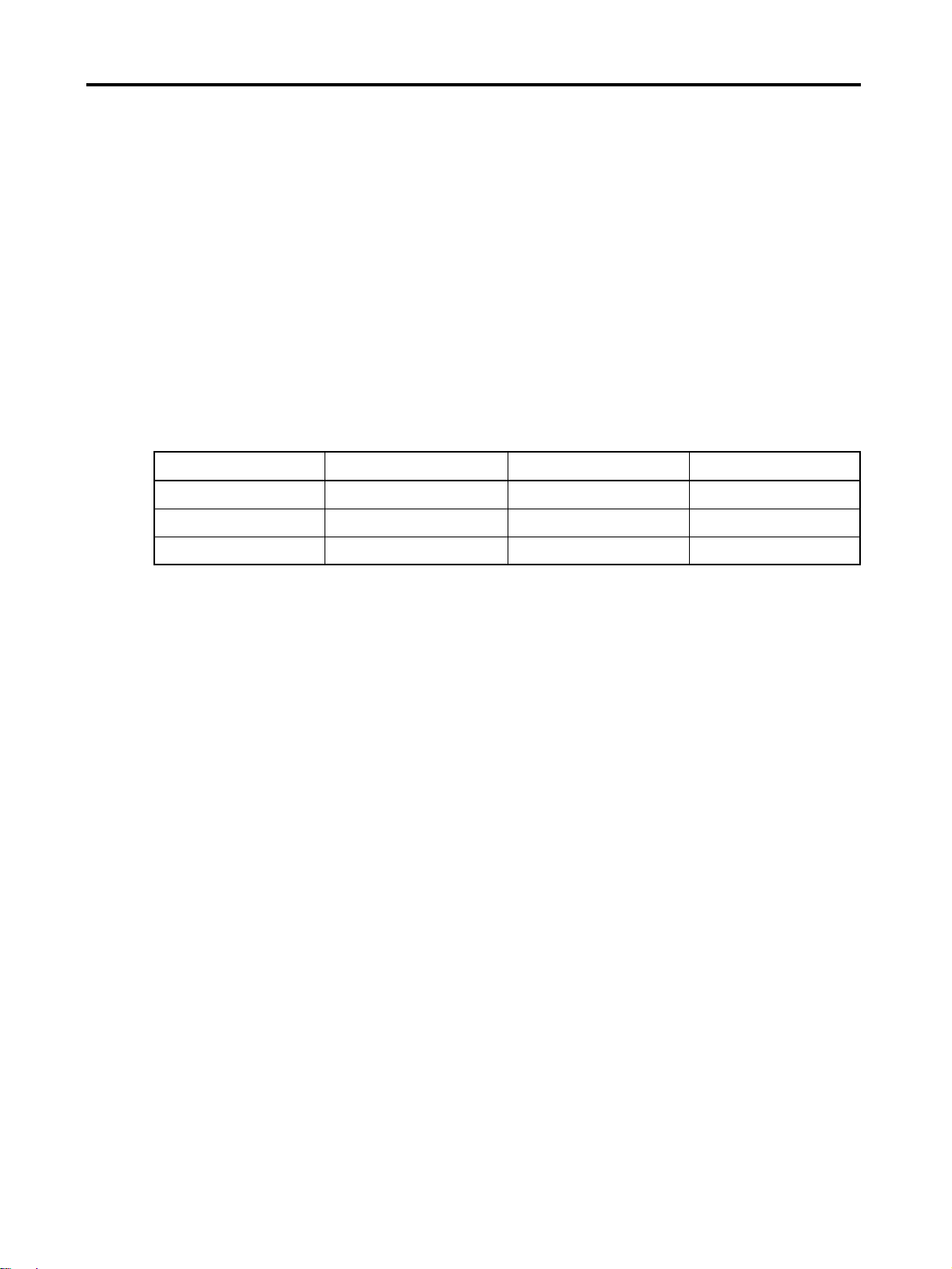
There are two regulators used in the phone to provide RF power. One is contained inside of
ADP3408 (U101), power management IC to provide the power for the VCTXO (X302). The other is
used to provide the power for remaining RF circuits.
Table 3-2.
Figure 3-5. Regulator Circuit.
3. TECHNICAL BRIEF
- 18 -
.
Regulator Voltage Powers Enable Signal
Regulator 1
(U1, 2V7_VTCXO)
2.7 V
0.5 V VCTXO
Regulator 2
(U414, RF2V8)
2.85 V
0.5 V RF circuitry VSYNTHEN
Page 20
3. TECHNICAL BRIEF
- 19 -
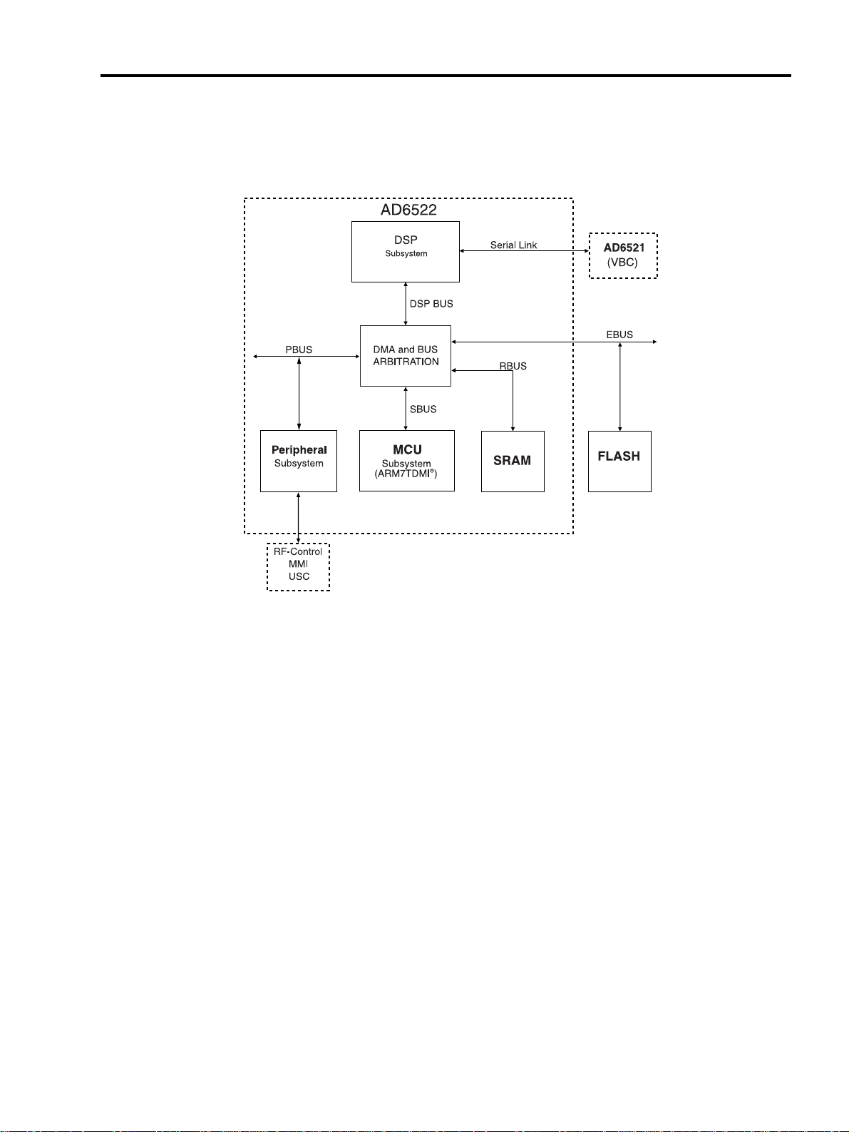
3.6 Digital Main Processor
The AD6522 is an ADI designed processor.
Figure 3-6. Top level block diagram of the AD6522 internal architecture.
BUS Arbitration Subsystem
It is to work as a cross point for data accesses between the three main busses. EBUS is for external
accesses, primarily from Flash memory for code and data. RBUS is for internal RAM access. PBUS
is for access to internal peripheral modules such as UART, RTC or SIM. In addition to the three
main system busses, it has SBUS, IOBUS and DMABUS.
DSP subsystem
It consists of ADI DSP, Viterbi coprocessor, Ciphering unit and a cache memory/controller system.
The DSP can run at a maximum clock frequency of 78 MHz at 2.45 V. The Viterbi and ciphering
accelerators enable a very efficient implementation of the channel equalization, encryption and
decryption tasks.
Page 21

3. TECHNICAL BRIEF
- 20 -
MCU subsystem
It consists of an ARM7TDMI central processing unit, a boot ROM, a clock generation and access
control module.
The maximum clock frequency for the ARM7TDMI is 39 MHz at 2.45 V.
The main clock is 13MHz and it is provided by VCTCXO. The Clock & BS(Bus Select) generator
make internal clock by multiplying the main clock by 1X, 1.5X, 2X and 3X.
The boot ROM contains MCU code for basic communication between the ARM and one of the serial
ports in the Universal System Connector subsystem.
Peripheral subsystem
It contains four major groups of elements.
The MMI group is a collection of all the functionality that are needed to implement a complete user
interface including keyboard, display, backlight, RTC, general purpose I/O etc.
House Keeping group consists of three different sub-modules: The Watch Dog Timer, the Interrupt
Controller, and the general timers.
GSM system group consists of the time base generation together with the synthesizer interface,
which form the radio control.
Direct Memory Access is located between the three system buses (PBUS, RBUS and EBUS) and
can move any data from any address location on one system bus to any address location on
another system bus.
Page 22
3. TECHNICAL BRIEF
- 21 -
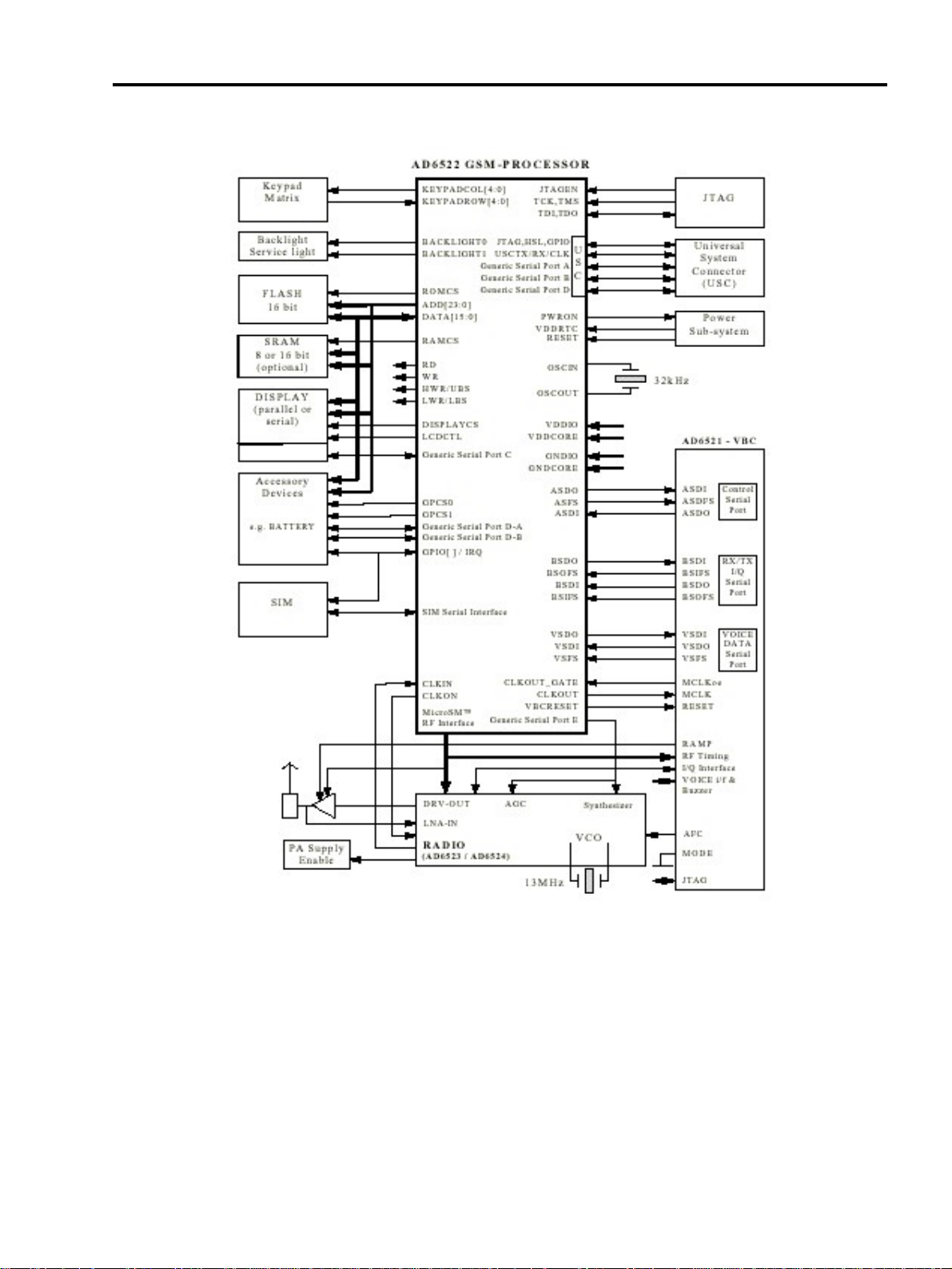
Figure 3-7. System interconnection of AD6522 external interfaces
Page 23
3. TECHNICAL BRIEF
- 22 -
Interconnection with external devices
RTC block interface
Countered by external X-TAL
The X-TAL oscillates 32.768KHz
LCD module interface
Controlled by LCD_MAIN/SUB_CS, LCD_RES, LCD_A0, /WR, /RD, DATA [00...07] ports
Table 3-3.
RF interface
The AD6522 control RF parts through TXEN, RXON1, RXON2, AGCEN, SDATA, SCLK, SEN etc.
Table 3-4.
Description
LCD_MAIN_CS
LCD_SUB_CS
LCD chip enable. Each LCD has CS pin
LCD_RES This pin resets LCD module.
LCD_A0
This pin determines whether the data to LCD module is display data or
control data
/WR, /RD Read/Write control
DATA [00...07] Parallel data line
Signal Name
Description
TXEN TX Enable/Disable
RXON1 LNA, Mixer1 On/Off
RXON2 Mixer 2 On/Off
AGCEN AGC Enable/Disable
SDATA Serial Data to PLL
SCLK Clock to PLL
SEN PLL Enable/Disable
Page 24
3. TECHNICAL BRIEF
- 23 -
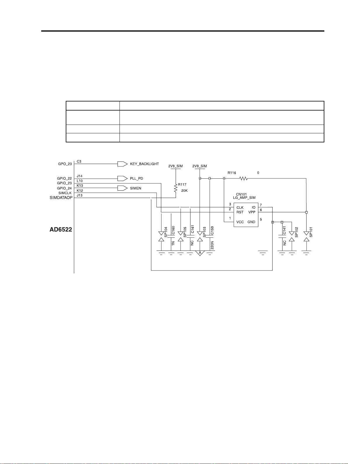
SIM interface
The AD6522 check status periodically in call mode if SIM card is inserted or not, but the AD6522
don't check in deep sleep mode.
Interface by SIM_IO, SIM_CLK, SIM_RST
Table 3-5.
Figure 3-8.
Key interface
Include 5 column and 5 row
The AD6522 detect key press by interrupt
ADP3408 interrupt
There are two interrupts EOC and CHARGEDETECT
EOC: End of Charge. Charging would be stopped when AD6522 receive this input.
CHARGEDETECT: This interrupt is generated when charge is inserted.
Description
SIM_IO
This pin receives and sends data to SIM card. G5200 support only 3.0
volt interface SIM card.
SIM_CLK Clock 3.5MHz frequency.
SIM_RST Reset SIM block.
Page 25
3. TECHNICAL BRIEF
- 24 -
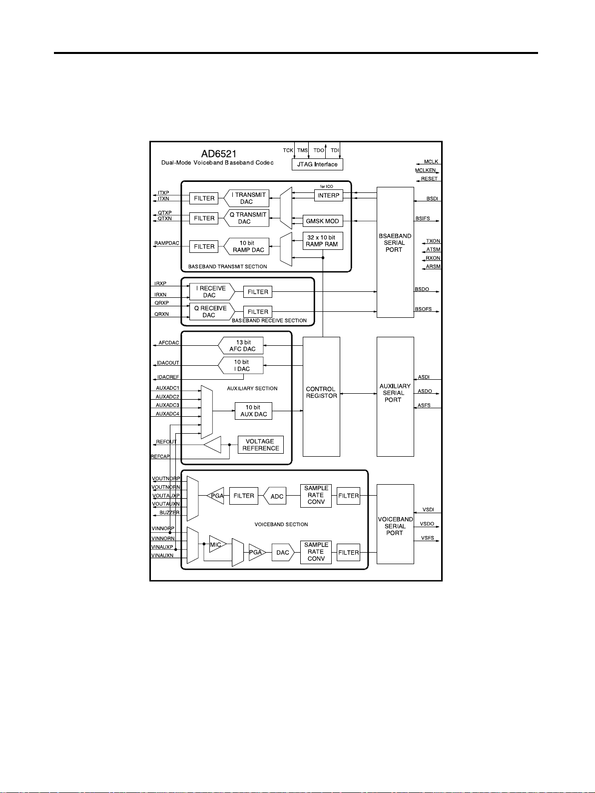
3.7 Analog Main Processor
AD6521
Figure 3-9. AD6521 function block diagram
Page 26

3. TECHNICAL BRIEF
- 25 -
BB Transmit section
This section generates in-phase and quadrature BB modulated GMSK signals (BT = 0.3) in
accordance with GSM 05.05 Phase 2 specifications
The transmit channel consists of a digital GMSK modulator, a matched pair of 10-bit DACs and a
matched pair of reconstruction filter
BB Receive section
This section consists of two identical ADC channels that process baseband in-phase(I) and
quadrature(Q) input signals.
Each channel consists of a coarse switched capacitor input filter, followed by a high-order sigmadelta modulator and a lowpass digital filter
Auxiliary section
This section contains two auxiliary DACs(AFC DAC, IDAC) for system control.
This section also contains AUX ADC and Voltage Reference
AUX ADC: 6 channel 10 bits
AFC DAC: 13 bits
IDAC: 10 bits
Voiceband section
Receive audio signal from MIC. G5200 use differential configuration.
Send audio signal to Receiver. G5200 use differential configuration.
It interconnect with external device like main microphone, main receiver, ear-phone and Hands free
kit
through the VINNORP, VINNORN, VOUTNORP, VOUTNORN, VINAUXP, VINAUXN,
VOUTAUXP, VOUTAUXN
VINNORP, VINNORN: Main MIC positive/negative terminal.
VOUTNORP, VOUTNORN: Main Receiver positive/negative terminal.
VINAUXP, VINAUXN: Hands free kit mic positive/negative terminal.
VOUTAUXP, VOUTAUXON: Hands free kit speaker positive/negative terminal.
Page 27
3. TECHNICAL BRIEF
- 26 -
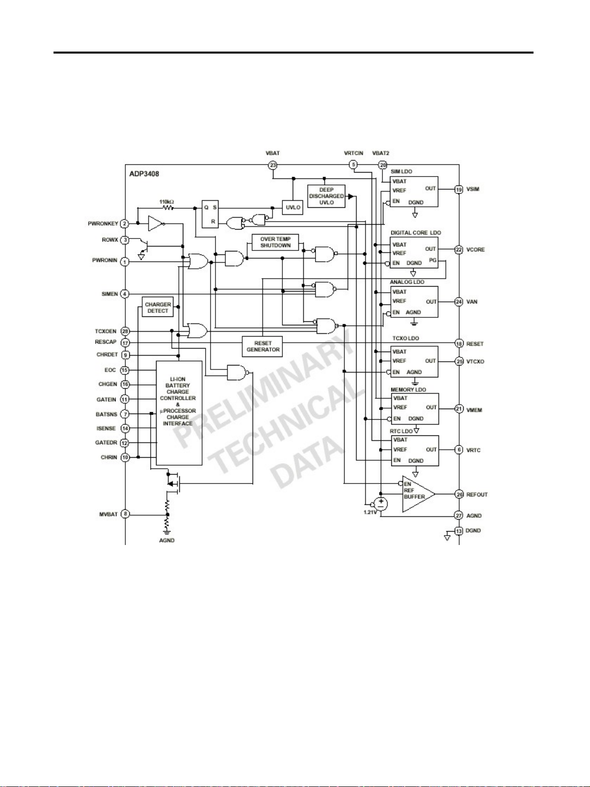
3.8 Power Management
ADP3408
Figure 3-10. ADP3408 inner block diagram.
Power up sequence logic
The ADP3408 controls power on sequence
Power on sequence
If a battery is inserted, the battery powers the 6 LDOs.
Then if PWRONKEY is detected, the LDOs output turn on.
REFOUT is also enabled
Reset is generated and send to the AD6522
Page 28
LDO block
There are 6 LDOs in the ADP3408
Table 3-6.
Battery charging block
It can be used to charge Lithium Ion and/or Nickel Metal Hydride batteries. G5200 use Li-Ion battery
only. Charger initialization, trickle charging, and Li-Ion charging control are implemented in
hardware.
Charging Process
Check charger is inserted or not
If ADP3408 detects that Charger is inserted, the CC-CV charging starts.
Exception: When battery voltage is lower than 3.2V, the precharge (low current charge mode) starts
firstly.
And the battery voltage reach to 3.2V the CC-CV charging starts.
Pins used for charging
CHARGERDETECT: Interrupt to AD6522 when charger is plugged.
CHARGEEN: Control signal from AD6522 to charge Li+ battery
EOC: Interrupt to AD6522 when battery is fully charged
GATEIN: Control signal from AD6522 to charge NiMH battery. But, not used.
MVBAT: Battery voltage divider. Divide ratio is 1:2.3 and it is sensed in AD6521 AUX_ADC
TA (Travel Adaptor)
Input voltage: AC 85V ~ 260V, 50~60Hz
Output voltage: DC 5.2V ( ±0.2 V )
Output current: Max 850mA ( ±50mA )
Battery
Li-ion battery (Max 4.2V, Nom 4.0V)
Standard battery : Capacity - 750mAh, Li-ion
3. TECHNICAL BRIEF
- 27 -
Description
VSIM 2.86 V (is provided to SIM card)
VCORE 2.45 V (is provided to the AD6522 & AD6521’s digital core)
VRTC 2.45 V (is provided to the RTC and Backup Battery)
VAN 2.45 V (is provided to the AD6521 I/O and used as microphone bias)
VTCXO 2.715 V (is provided to VCTCXO)
VMEM 2.80 V (is provided to Flash)
Page 29
3. TECHNICAL BRIEF
- 28 -
3.9 Memories
64M flash memory + 16M SRAM
16 bit parallel data bus
ADD01 ~ ADD21.
RF Calibration data are stored in Flash
3.10 Display and Interface
Table 3-7
G5200 has dual type LCD. There are the control output LCD_MAIN/SUB_CS which is derived from
AD6522, this acts as the chip select enable for the Main/Sub LCD. AD6522 uses DATA[00:07] pins
to send data for displaying graphical text onto the each LCD ( Main/Sub ).
Main LCD Sub LCD
Display Format 128 x 128 dots 96 x 64 dots
Back light EL Backlight EL Backlight
Page 30
3. TECHNICAL BRIEF
- 29 -
3.11 Keypad Switches and Scanning
The key switches are metal domes, which make contact between two concentric pads on the
keypad layer of the PCB when pressed. There are 25switches (S301-S325), connected in a matrix
of 5 rows by 5 columns, as shown in Figure, except for the power switch (S310), which is connected
independently.
Functions, the row and column lines of the keypad are connected to ports of AD6522. The columns
are outputs, while the rows are inputs and have pull-up resistors built in. When a key is pressed, the
corresponding row and column are connected together, causing the row input to go low and
generate an interrupt. The columns/rows are then scanned by AD6522 to identify the pressed key.
Figure 3-11. Keypad Switches and Scanning.
DOWN
0
Page 31

3. TECHNICAL BRIEF
- 30 -
3.12 Microphone
The microphone is soldered to the main PCB. The audio signal is passed to VINNORP (#K8) and
VINNORN (#K7) pins of AD6522. The voltage supply 2V45_VCORE is output from ADP3408, and is
a bias voltage for both the VINNOR (through R105) and VINAUX (through R104) lines.
The VINNOR or VINAUX signal is then A/D converted by the Voiceband ADC part of AD6521.
The digitized speech is then passed to the DSP section of AD6522 for processing (coding,
interleaving etc.).
Figure 3-12. Microphone.
Page 32

3. TECHNICAL BRIEF
- 31 -
3.13 Earpiece
The earpiece is driven directly from AD6521 VOUTNORP (#K8) and VOUTNORN (#K7) pins and
the gain is controlled by the PGA in an AD6521. The earpiece is located in the handset floder front
panel, and the signals are routed to it via FPCB connector between Main Board and FPCB board.
But, The VOUTNORP signal has to be selected by the control signal “SPK_EN”. If SPK_EN is low,
VOUTNORP is directly connected to the Earpiece, else VOUTNOTP is connected to the Midi
Chip(U203).
Figure 3-13. Earpiece & Handsfree Interface
Page 33

3. TECHNICAL BRIEF
- 32 -
3.14 Hands-free Interface
The audio out (VOUTAUXP & VOUTAUXN) to the hands-free kit consists of a pair of differential
signals from AD6521 auxiliary outputs (#K9, #K6), which are tracked down the board to carkit
connector (CN301) at the base of the handset. The DC level of the signal is supplied to the
VOUTAUX pin. And the EXT_IN signal is then input to the VINAUXP (#H10) and VINAUXN (#G10)
of AD6521.
3.15 Headset Jack Interface
Headset Jack has the single-end structure in both audio in and out. The audio out to the headset
jack is used only one line(VOUTAUXP/HEADSET_SPK_P1) which can be connected to the
HEADSET_MIC_P or HFK_SPK_P by the analog switch(U204). If you put in the headset jack in the
top of the handset, HEADSET_SPK_P1(VOUTAUXP) is connected to the HEADSET_SPK_P. And
the audio in from the headset jack has also one line(VINAUXP/HEADSET_MIC_P). If the headset
jack is put in, HEADSET_MIC_P is input from the MIC of headset jack, else HEADSET_MIC_P is
connected to HFK_MIC_P which is input from the Hands-free Kit.
3.16 Key Back-light Illumination
In key back-light illumination, there are 12 Blue LEDs in Main Board, which are driven by
KEY_BACKLIGHT line from AD6522.
Figure 3-14. Key Back-light Illumination.
Page 34

3. TECHNICAL BRIEF
- 33 -
3.17 LCD Back-light Illumination
In LCD Back-light illumination, there is an EL driver in sub LCD side of LCD Module, which is driven
by BACKLIGHT(EL_EN) line from AD6522.
Figure 3-15. LCD Back-light Illumination.
3.18 Multi-Color LED Illumination
In multi-color LED illumination, there is an LED chip and three TRs in sub LCD side of LCD Module,
which is driven by LED_G, LED_B and LED_Main line from AD6522.
Figure 3-16. Multi-Color LED
Page 35

3. TECHNICAL BRIEF
- 34 -
3.19 Speaker & MIDI IC
Figure 3-17. Speaker & MIDI IC
MA-3 is a synthesizer LSI for mobile phones that realize advanced game sounds. This LSI has a
built-in speaker amplifier, and thus, is an ideal device for outputting sounds that are used by mobile
phones in addition to game sounds and ringing melodies that are replayed by a synthesizer.
The synthesizer section adopts “stereophonic hybrid synthesizer system” that are given advantages
of both FM synthesizers and Waveform table synthesizers to allow simultaneous generation of up to
thirty-two FM tones and eight Waveform table tones.
Since FM synthesizer is able to present countless tones by specifying parameters with only several
tens of bytes, memory capacity and communication band can be saved, and thus, the device
exhibits the features in operating environment of mobile phones such as allowing distribution of
arbitrary melodies with tones. On the other hand , since Waveform table synthesizer complies with
downloading of tones from host CPU, arbitrary ADCM/PCM tones can be treated from sequencer in
addition to the use of tones that are built-in the LSI.
MA-3 has a built-in circuit for controlling vibrators and LEDs synchronizing with play of music.
Page 36

- 35 -
4. TROUBLE SHOOTING
4. TROUBLE SHOOTING
4.1 RF Components
RF components
Reference Description Reference Description
U401 AND Gate U412 APC IC
U405 Antenna Switch U413 Inverter
U407 DCS RF SAW Filter U414 LDO
U408 GSM RF SAW Filter SW401 Mobile Switch
U409 PAM Y401 TXVCO
U411 RF Main Chip N401 Coupler
SW401
N401
N409
U412
Y401
U413
U401
U414
U407
U411
U408
U405
Page 37

4. TROUBLE SHOOTING
- 36 -
RX Check Area
Page 38

4. TROUBLE SHOOTING
- 37 -
4.1-1 Checking Regulator Circuit
U414.1
U414.6
Page 39

4.1-2 Checking VCTCXO Circuit
Graph 4-1. VCTCXO 13MHz Graph 4-2. VCTCXO 2.7V
4. TROUBLE SHOOTING
- 38 -
Y401.3
Y401.4
Page 40

4. TROUBLE SHOOTING
- 39 -
4.1-3 Checking Control Signal
TP409(LE)
TP407(Data) TP408(Clock)
TP4043(RXEN)
Graph 4-3. RF Control Signal
Page 41

4. TROUBLE SHOOTING
- 40 -
4-1-4 Checking Ant SW & Mobile SW
U401.1
U401.6
R405
SW401.2
SW401.1
U405.11
U405.10 U405.2
U405.1
Table 4-1. ANT SW Control Logic
Page 42

4. TROUBLE SHOOTING
- 41 -
Graph 4-4. ANT SW Control
GSM. DCS RX Mode
Graph 4-5. Dual AND Gate input
For GSM RX Mode
Table 4-2. ANT SW Control Logic
Graph 4-6. Dual AND Gate input
For DCS RX Mode
Page 43

4. TROUBLE SHOOTING
- 42 -
4-1-5 Checking Saw Filter Circuit
U407.3 U407.1 U408.3 U408.1
Page 44

4. TROUBLE SHOOTING
- 43 -
4-1-6 Checking RX IQ
RXIN RXQN
RXIP RXQP
Graph 4-7. RX IQ Signal Graph 4-8. RX I Signal (Extended)
Page 45

4.2 Tx Trouble
- 44 -
4. TROUBLE SHOOTING
6
1
3
3
4
2
5
Rx Check Area
Page 46

- 45 -
4. TROUBLE SHOOTING
4-2-1 Checking Regulator Circuit
If you already Check this point while checking RX part, You can Skip this Test
U414. 2
U414.1
U414.6
Page 47

- 46 -
4. TROUBLE SHOOTING
4-2-2 Checking VCTCXO Circuit
If you already Check this point while checking RX part, You can Skip this Test
Graph 4-9. VCTCXO 13MHz Graph 4-10. VCTCXO 2.7V
Y401. 3
Y401. 4
Page 48

- 47 -
4. TROUBLE SHOOTING
4-2-3 Checking Control Signal.
Graph 4-11. RF Control Signal Graph 4-12. TXEN, TXRAMP, TXPA
TP409(LE)
TP407(Data)
TP408(Clock)
TXPA
(R405)
TXEN
(R425)
TXRAMP
(R427)
Page 49

- 48 -
4. TROUBLE SHOOTING
4-2-4 Checking TX IQ
C463
100P
TXQN
TXQP
TXIN
TXIP
C464
100P
TXQN TXIN
TXQP TXIP
Graph 4-13. TX IQ Signal
Page 50

- 49 -
4. TROUBLE SHOOTING
4-2-5 Checking RF TX Level
N401. 3
U409. 1
R407
R411
U409. 8
R472
N401. 1
L405
L408
C432
U412. 1
Page 51

- 50 -
4. TROUBLE SHOOTING
4-2-6 Checking Ant SW & Mobile SW
SW401. 2
SW401. 1
U405. 11
U405. 2
U405. 8 U405. 5
U405. 3
U401. 1
R405
U401. 6
Table 4-1. ANT SW Control Logic
Page 52

4-2-6 Checking Ant SW & Mobile SW
Graph 4-14. ANT SW Control Graph 4-15. ANT SW Control
DCS TX Mode GSM TX Mode
Graph 4-16.Dual AND Gate input Graph 4-17.Dual AND Gate input
For DCS TX Mode For GSM TX Mode
Table 4-3. ANT SW Control Logic
- 51 -
4. TROUBLE SHOOTING
Page 53

- 52 -
4. TROUBLE SHOOTING
4-2-7 Receiver RF Level
GSM : CH.62, -60dBm
DCS :CH.699, -60dBm
Page 54

- 53 -
4. TROUBLE SHOOTING
Test Points of Rx Level
13
4
2
Page 55

4. TROUBLE SHOOTING
- 54 -
4-2-8 Transmitter RF Level
GSM
TXVCO
REFCLK
Base
BaseBase
Base
Band
BandBand
Band
Block
BlockBlock
Block
DCS : X7X0 ~ X785MHz
DCS : X7X0 ~ X785MHzDCS : X7X0 ~ X785MHz
DCS : X7X0 ~ X785MHz
GSM : 880 ~ 9 X5MHz
GSM : 880 ~ 9 X5MHzGSM : 880 ~ 9 X5MHz
GSM : 880 ~ 9 X5MHz
X3MHz
90
0
LF
TXIP
TXIPTXIP
TXIP
TXIN
TXINTXIN
TXIN
TXQP
TXQPTXQP
TXQP
TXQN
TXQNTXQN
TXQN
PFD
Fractional-N
PLL
PLL_LE
PLL_LEPLL_LE
PLL_LE
PLL_CLK
PLL_CLKPLL_CLK
PLL_CLK
PLL_DATA
PLL_DATAPLL_DATA
PLL_DATA
Serial
SerialSerial
Serial
I/O
I/OI/O
I/O
/D2
/DX
X2
DCS
/R
f
vco = (N+3.5+FN/2^22)
f
ref/R
f
vco
f
ref
/3
X2
TXEN
TXENTXEN
TXEN
RXEN
RXENRXEN
RXEN
PLL_PD
PLL_PDPLL_PD
PLL_PD
Serial
SerialSerial
Serial
I/O
I/OI/O
I/O
FEENA
FEENAFEENA
FEENA
BANDSEL2
BANDSEL2BANDSEL2
BANDSEL2
BANDSELX
BANDSELXBANDSELX
BANDSELX
LF
f
TX
f
f
LO
AFC
AFCAFC
AFC
X3MHz
X3MHzX3MHz
X3MHz
2V7_VTCXO
2V7_VTCXO2V7_VTCXO
2V7_VTCXO
COUPLER
(LDCX5D)
PAM(PF08X22B)
ANT
S/W
LMG002S
GSMSEL
GSMSELGSMSEL
GSMSEL
DCSSEL
DCSSELDCSSEL
DCSSEL
TXPA
TXPATXPA
TXPA
VCX
VCXVCX
VCX
VC2
VC2VC2
VC2
GSM : 975(-300mV) ~ X24(300mV)
DCS : 5X2(-750mV) ~ 885(750mV)
ATT
ATT
APCIC(AD83X5)
TXRAMP
TXRAMPTXRAMP
TXRAMP
TXEN
TXENTXEN
TXEN
X0dBm
8dBm
2dBm
0dBm
6
32dBm
34dBm
GSM : 32dBm
DCS : 29dBm
3X.5dBm
33.5dBm
ATT
GSM : X5dBm
DCS : X8dBm
GSM : -6dBm
DCS : -3dBm
1
3
1
3
5
11
87
109
12
2
4
GSM : 32.5dBm
DCS : 29.5dBm
Mobile
S/W
GSM :Pwr Lvl 5,CH.62,32dBm
DCS :Pwr Lvl 5,CH.699, 29dBm
Page 56

4. TROUBLE SHOOTING
- 55 -
4-2-8 Transmitter RF Level
Test Points of Tx Level
13
11 5
3
1
2
4
6
12
7 , 8 9 , 10
Page 57

4. TROUBLE SHOOTING
- 56 -
4-2-9 Test Points for RF Components
Test Points for RF components
VC2
U401. 3
VC1
U401. 7
TXPA
(R405)
TXQN
TXQP
RXQN
RXQP
2V7_VCTCXO
13MHz CLock
TXRAMP(R427)
TXEN(R425)
TXIN
TXIP
RXIN
RXIP
RF 2.85V
Page 58

• Test Points for RF Components
Test Points for RF components
(Keypad Side/Lower)
4. TROUBLE SHOOTING
- 57 -
TP408(PLL_Clock)
TP409(PLL_LE)TP409(PLL_LE)
TP407(PLL_Data)
Page 59

4. TROUBLE SHOOTING
- 58 -
• Baseband components (Component Side)
Baseband components (Component Side)
U105
U106
CN302
U101
U103
X101
U203
U204
U302
U202
U205
Q302
CN101
U201
D102
D101
U102
Reference Description Reference Description
U101 PMIC U205 LDO
U102 P-Channel FET U302 Analog Switch
U103 Analog Main Processor D101 Diode
U105 Digital Main Processor D102 Dual Diode
U106 Memory X101 X-TAL
U201 Comparator Q302 Dual Transistor
U202 Analog Switch CN101 SIM Connector
U203 MIDI IC CN301 IO Connector
U204 Analog Switch
Page 60

• Baseband components (Keypad Side)
Baseband components (Keypad Side)
4. TROUBLE SHOOTING
- 59 -
Q101
MIC101
U301
Q301
D301
Reference Description Reference Description
U301 Hall Sensor D301 Dual Diode
Q301 Transistor MIC101 C-MIC
Q302 Transistor
Page 61

4.3 Power on Trouble
- 60 -
4. TROUBLE SHOOTING
Setting : Connect PIF, and set remote switch off at PIF.
Page 62

- 61 -
4. TROUBLE SHOOTING
POWER-ON KEY
signal input
This signal should go HIGH when the power-on
procedure is completed.
Pin 25 (VTCXO=2.7V) Pin 22 (VCORE=2.45V)
Pin 21 (VMEM=2.8V)
Pin 6 (VRTC>1.2V)
Pin 2 (Power Key)
Pin 1 (PWRON_EN)
These powers should
be necessary to
power on.
Page 63

- 62 -
4. TROUBLE SHOOTING
4.4 Charging Trouble
Setting : Connect PIF, and set remote switch off at PIF.
Page 64

- 63 -
4. TROUBLE SHOOTING
The charging current
will flow into this
direction.
R102
D101
U102
Page 65

4. TROUBLE SHOOTING
- 64 -
4.5 LCD Trouble
Setting : Connect PIF and power on.
Page 66

4. TROUBLE SHOOTING
- 65 -
Soldering Check
If the FPCB has a problem, the
control signals for LCD cannot
be transmitted properly.
CN301
Page 67

4. TROUBLE SHOOTING
- 66 -
4.6 Receiver Trouble
Setting : After initializing GSM MS test equipmemt, connect PIF and power on. Make a test call to 112.
Set audio part at test equipment as PRBS or continuous wave, not echo. Set the volumn max.
Page 68

The Circuit Diagram of the receiver path. Refer to page 2 of the complete circuit diagram for detail.
4. TROUBLE SHOOTING
- 67 -
RECEIVER
PMIC (U101)
C206
U202. 4
U202. 5
YMU762 (U203)
Soldering
Check
From the
U103(AD6521)
U202
C206
From the
U103(AD6521)
To Receiver at
LCD module via
CN301
Page 69

4. TROUBLE SHOOTING
- 68 -
The waveforms of the audio signals at each point
U202. 4
U202. 5
C206
(REC-)
Page 70

4. TROUBLE SHOOTING
- 69 -
4.7 Speaker Trouble
Setting : Connect PIF to the phone, and power on. Enter the engineering mode, and set "Melody on" at
"BB Test-Buzzer" menu.
Page 71

4. TROUBLE SHOOTING
- 70 -
U203
Pin 26
Pin 25
U205
C221
R222, R227
Soldering Check
in LCD Module
Speaker
C209, C211, R213, R215
CN301
Page 72

The circuit diagram of the part of the melody IC. Refer to the page 2 of the complete circuit diagram for
detail.
4. TROUBLE SHOOTING
- 71 -
C209, R213, C211, R215
These four components make up the
analog amplifier stage of melody.
U203
U205
C221
R227 R222
This is the melody IC.
To the speaker at LCD
module via CN301.
The Power for analog part of the
melody IC. The voltage is 3.3V
The Power for digital part of the
melody IC. The voltage is 2.8V.
It is from the PMIC(ADP3408, U101)
Page 73

4.8 Mic Trouble
4. TROUBLE SHOOTING
- 72 -
Setting : After initializing GSM MS test equipment, connect PIF to the phone, and power on. Make a test
call to 112. Make a sound in front of microphone.
Page 74

4. TROUBLE SHOOTING
- 73 -
C118
R105 R108
R110
R112
Q101.3
MIC101
C132 C129
Page 75

4. TROUBLE SHOOTING
- 74 -
The waveforms at MIC+ and MIC-
R105
R108
MIC+
MIC+
MIC-
MIC-
C118
MIC101
The voltage at this point
goes to almost 0V when
the mic is activated.
Mic activating signal
Mic is activated when this
signal goes to HIGH
R110, R112
C129, C132
The signal flow of
the microphone to
U103(AD6521)
Page 76

4. TROUBLE SHOOTING
- 75 -
4.9 Vibrator Trouble
Setting : Connect PIF to the phone, and power on. Enter the engineering mode, and set "Vibrator On" at
"BB Test-Vibrator" menu.
START
Is the voltage at pin 3
of Q301 near 0V?
Yes
Check the soldering of R301
Yes
Check the soldering of CN301
Yes
Check the soldering of
vibratior at LCD module
No
Check the soldering of R309.
Replace Q301.
No
No
No
Yes
Resolder R301.
Resolder CN301.
Resolder vibrator.
No
Resolder R309.
Yes
Replace Vibrator.
VIBRATOR WILL
WORK PROPERLY.
Page 77

4. TROUBLE SHOOTING
- 76 -
Pin 22
CN301
Soldering Check
in LCD Module
Vibrator
R301
Q301.3
Q301.2
From the vibrator at
LCD module via CN301.
When the vibrator works,
the voltage at this point
goes to almost 0 V.
When the vibrator
works, the current flow
in this directoin.
When the vibrator
works, the signal at this
point goes to 2.8V.
R309
Page 78

4. TROUBLE SHOOTING
- 77 -
4.10 Backlight Trouble
Setting : Connect PIF to the phone, and power on. Enter engineering mode, and set "Backlight on" at
"BB test-Backlight" menu.
Page 79

4. TROUBLE SHOOTING
- 78 -
Q302.2R321
R319
Page 80

4. TROUBLE SHOOTING
- 79 -
4.11 Folder on/off Trouble
Setting : Connect PIF to the phone, and power on.
Page 81

4. TROUBLE SHOOTING
- 80 -
R310
The voltage at this point
goes from 2.8V to 0 V
when the folder is closed.
To U105(AD6522)
This component operate
when a magnet get close
here.
U301.1
U301.2
Page 82

4. TROUBLE SHOOTING
- 81 -
4.12 SIM Detect Trouble
Setting : Insert the SIM into CN101. Connect PIF to the phone, and power on.
Page 83

4. TROUBLE SHOOTING
- 82 -
PIN 5
PIN 3
PIN 1
PIN 7
Page 84

4. TROUBLE SHOOTING
- 83 -
4.13 Earphone Trouble
Setting : After initializing GSM test equipment, connect PIF to the phone and power on.
Page 85

4. TROUBLE SHOOTING
- 84 -
Page 86

4. TROUBLE SHOOTING
- 85 -
Page 87

4. TROUBLE SHOOTING
- 86 -
Page 88

4. TROUBLE SHOOTING
- 87 -
4.14 HFK Trouble
C168
U201.1
R208 R209
R212R210
R211
R230, R231
R104
C117
C124
R201 CN201
L201
U204.1
U204.5
U204.6
R103
R106
Page 89

4. TROUBLE SHOOTING
- 88 -
This part makes the
mic bias of the ear-mic.
The direction of the audio
To U103(AD6521)
The voltage input of
ear-mic hook-detect
The voltage input of
ear-mic detect
The reference voltage
for the hook-detect of
The signal flow when the
ear-mic is activated.
U204 selects the path of audio
signal for the ear-mic or the HFK.
The circuit diagram of the ear-mic jack
Refer to the page 2 of the complete circuit diagram for detail.
Refer to the page 2 of the complete circuit diagram
for detail.
The reference voltage
for the detect of earmic.
These resistors make
the reference voltage.
Mic bias and path for the ear-mic
Refer to the page 1 of the complete
circuit diagram for detail.
Ear-mic detection part
Refer to the page 2 of the complete
circuit diagram for detail.
Page 90

4. TROUBLE SHOOTING
- 89 -
Setting : After initializing GSM test equipment, connect PIF to the phone and power on.
Page 91

4. TROUBLE SHOOTING
- 90 -
Page 92

4. TROUBLE SHOOTING
- 91 -
Page 93

4. TROUBLE SHOOTING
- 92 -
R333 U204.1
U204
U204.5
CN302
C117
C124
CN201
L201
R205
R328
2.8V
R158
R106
R103
R104
C168
CN302.1
R156
C171
R170
CN302.9 ~
CN302.12
Check Point
( 0V when HFK is
activated.)
Page 94

4. TROUBLE SHOOTING
- 93 -
The HFK detect signal
R328
R333
CN302
The audio signals
from & to the HFK
The HFK detect signal
This point goes to
0 V when the HFK
is activated.
The circuit diagram of the part of CN302
Refer to the page 3 of the complete circuit diagram.
The HFK detect signal input to U105 (AD6522)
Refer to the page 1 of the complete circuit diagram.
Page 95

4. TROUBLE SHOOTING
- 94 -
The direction of the audio
signal from the mic of the HFK
The audio signal from the mic of the HFK to U103(AD6521)
This part is same with that of the ear-mic.
Refer to the page 1 of the complete circuit diagram for detail.
The signal flow when
the HFK is activated.
U204 selects the path of audio
signal for the ear-mic or the HFK.
Refer to the page 2 of the complete circuit diagram
for detail.
To U103
(AD6521)
Page 96

5. ASSEMBLY INSTRUCTION
- 95 -
5. ASSEMBLY INSTRUCTION
5.1 Disassembly
1. Remove the battery, antenna and screws as shown above.
Figure 5-1. Removing Battery pack, screws and Antenna
2. Carefully lift up the bottom of Rare Cover first, then hold the covers and twist them.
Figure 5-2. Disassembly of Rear cover and Front cover
1
2
3
Page 97

5. ASSEMBLY INSTRUCTION
- 96 -
3.Finally carefully remove the rear-cover from the hooks on the top of front-cover.
Figure 5-3. Disassembly from the hooks
Page 98

5. ASSEMBLY INSTRUCTION
- 97 -
4. Remove the pin shown below to unlock the PCB.
Figure 5-4. Unlocking and removing the PCB
Page 99

5. ASSEMBLY INSTRUCTION
- 98 -
5. Use a sharp awl to push away the antenna-bushing.
Figure 5-5. Removing Antenna-bushing
6. Use a tweezers to remove the Battery Locker.
Figure 5-6. Removing battery locker
3
1
1
2
Page 100

5. ASSEMBLY INSTRUCTION
- 99 -
7. Remove the buttons.
Figure 5-7. Removing buttons
8. Push away the hinge to remove the folder.
Figure 5-8. Detaching Folder
 Loading...