

LG VM101 Service Manual
Features of LG-VM101
1. Wave Type
PCS : G7W
•
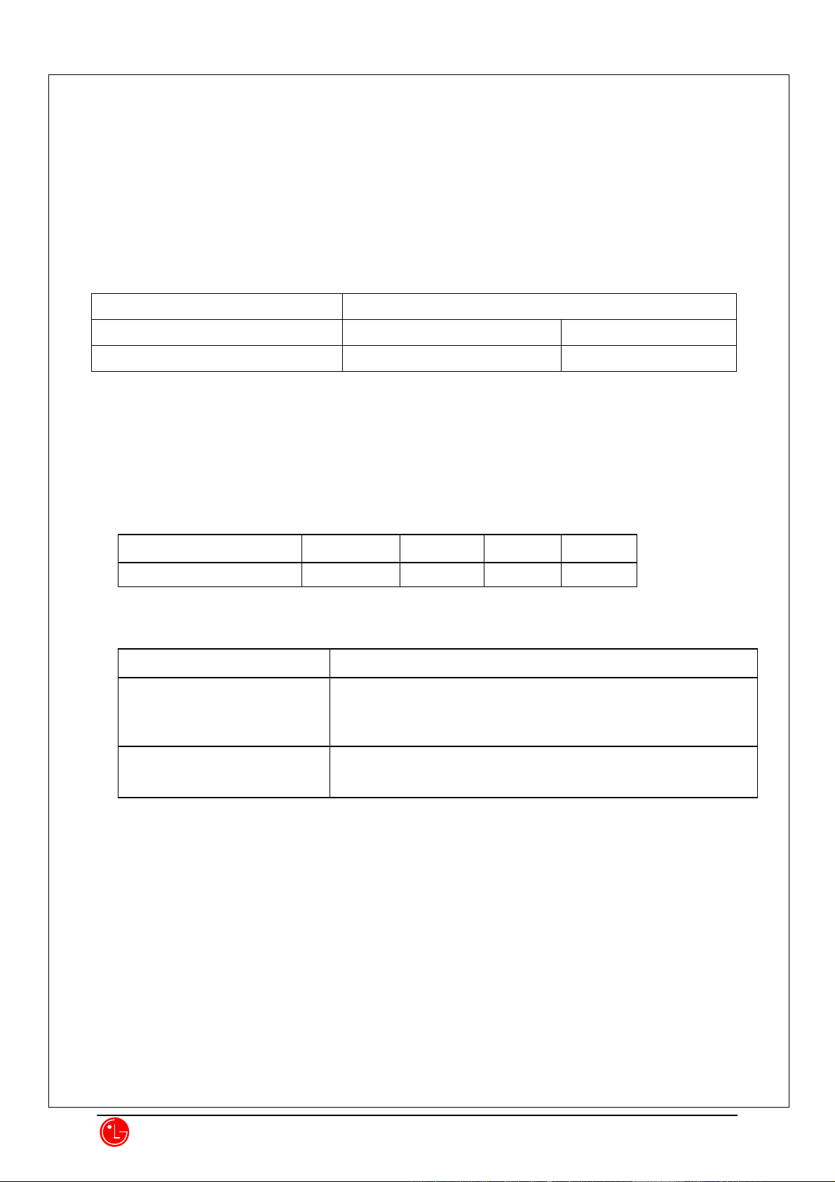
2. Frequency Scope
Transmit Frequency (MHz)
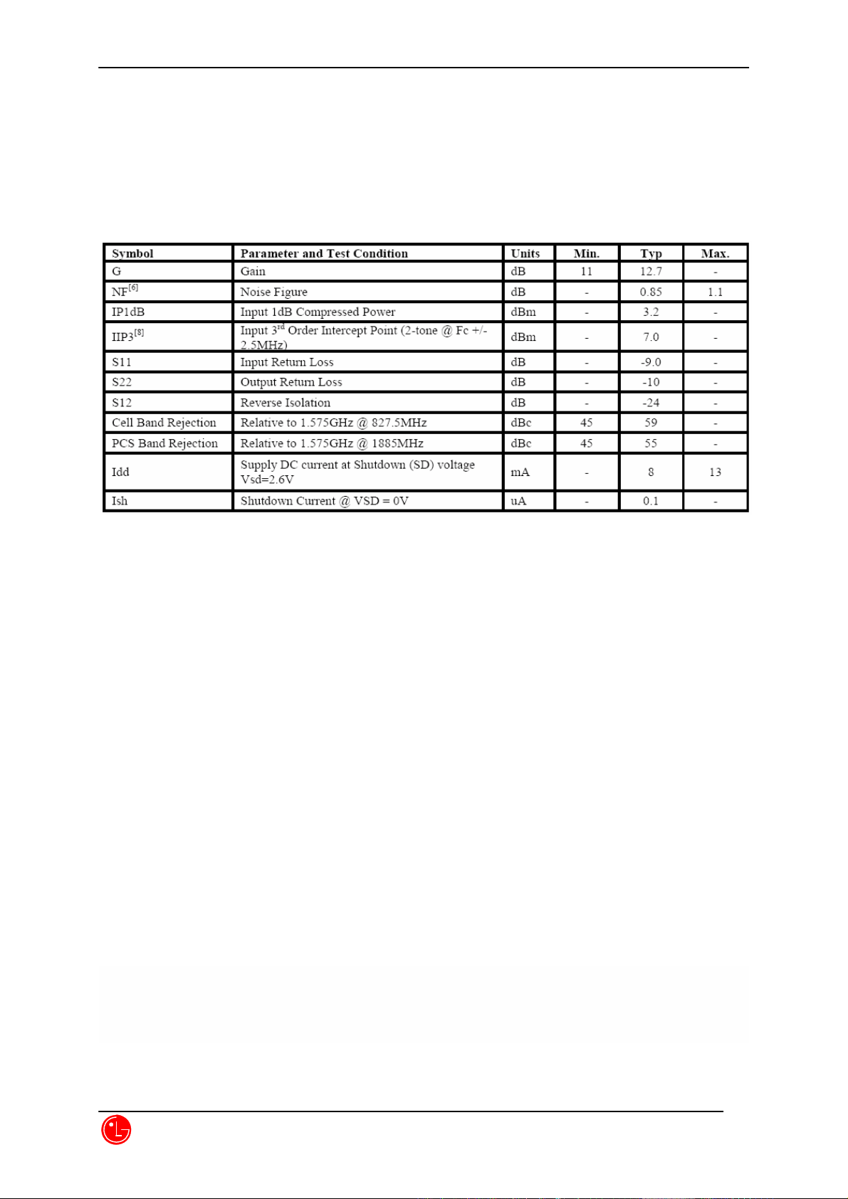
3. Rated Output Power : PCS = 0.240W
4. Output Conversion Method : This is possible by correcting the key board channel.
5. Voltage and Current Value of Termination Part Amplifier (Catalogue included)
Receive Frequency (MHz)
PCS PCS GPS
1850~1910 1930~1990 1575.42
MODE
Part Name Voltage Current Power
6. Functions of Major Semi-Conductors
PCS AWT6321R 4.2V 600mA 0.240W
Classification Function
QSC6055 Terminal operation control and digital signal processing
MCP (K5E1H12ACM-D075) NAND (1Gbit) + DDR (512Mbit)
7. Frequency Stability
•
PCS : ±0.1PPM
LG Electronics Inc.
Converts RF signal to baseband signal
Converts baseband signal to RF signal
Storing of terminal operation program
L
LG-VM101
CDMA Mobile Subscriber Unit
LG-VM101
SERVICE MANUAL
Dual BAND, Dual MODE
[PCS/GPS]
CDMA MOBILE PHONE
1
G Electronics Inc.
1

LG-VM101
General Introduction ..............................4
Chapter 1. System Introduction ............5
1. System Introduction..............................5
1.1 CDMA Abstract...............................5
2. Features and Advantages of CDMA
Mobile Phone .......................................6
2.1 Various Types of Diversities ...........6
2.2 Power Control ................................6
2.3 Voice Encoder and Variable Data
Speed .............................................7
2.4 Protecting Call Confidentiality ........7
2.5 Soft Handoff ...................................8
2.6 Frequency Re-Use and Sector
Segmentation .................................8
2.7 Soft Capacity..................................8
3. Structure and Functions of Dual-band
CDMA Mobile Phone............................9
4. Specification .......................................10
4.1 General Specification ...................10
4.1.1 Transmit/Receive Frequency
Interval ............................................10
4.1.2 Number of Channels (Channel
Bandwidth) ......................................10
4.1.3 Operating Voltage ...........................10
4.1.4 Battery Power Consumption ...........10
4.1.5 Operating Temperature ............. ......10
4.1.6 Frequency Stability .........................10
4.1.7 Antenna...........................................10
4.1.8 Size and Weight .............................10
4.1.9 Channel Spacing ...... ................... ...10
4.1.10 Battery Type, Capacity and
Orerating Time ..............................11
4.2 Receive Specification ...................11
4.2.1 Frequency Range ...........................11
4.2.2 Local Oscillating Frequency Range 11
4.2.3 Sensitivity ................ .................. ......11
4.2.4 Selectivity .......... ............... ............ ...11
4.2.5 Interference Rejection ............... ......11
4.2.6 Spurious Wave Suppression...........11
4.2.7 CDMA Input Signal Range .............12
4.3 Transmit Specification ..................12
4.3.1 Frequency Range ...........................12
4.3.2 Local Oscillating Frequency Range ...12
4.3.3 Intermediate Frequency.............. ....12
4.3.4 Output Power............... .................. .12
4.3.5 CDMA TX Frequency Deviation ......12
4.3.6 CDMA TX Conducted Spurious
Emissions .......................................12
4.3.7 CDMA Minim u m T X P o w er Cont r o l ...12
4.4 MS (Mobile Station) Transmitter
Frequency ....................................13
4.4.1 PCS mode ......................................13
4.5 MS (Mobile Station) Receiver
Frequency ....................................14
4.5.1 PCS mode ......................................14
4.5.2 GPS mode : 1575.42MHz ..............14
4.6 AC Adaptor ...................................15
4.7 Cigar Lighter Charger ..................15
4.8 Hands-Free Kit .............................15
5. Installation ............. .............................15
5.1 Installing a Battery Pack ..............15
5.2 For Adapter Use ...........................15
5.3 For Mobile Mount .........................15
5.3.1 Installation Position............. ............15
5.3.2 Cradle Installation ............... ............15
5.3.3 Interface Box ..................................16
5.3.4. Microphone Installation..................16
5.3.5 Cable Connections ..... .................. ..16
Chapter 2. NAM Input Method .............17
NAM Programming Method and
Telephone Number Input Method .......17
PREPARATION ......................................17
PROGRAMMING STEPS ......................17
Chapter 3. Circuit Description ............18
2
LG Electronics
Inc.
2
2

LG-VM101
1. RF Transmit/Receive Part ..................18
1.1 Overview ......................................18
1.2 Description of Rx Part Circuit.......18
1.2.1 Saw Filter (F1101) .... .....................18
1.2.2 Duplexer .........................................19
1.2.3 LNAs (U2101) ............. ............... .....19
1.2.4 GPS LNA (U1402) ..........................21
1.2.5 Down-converter Mixers............. ......21
1.2.6 Rx RF SAW Filters (F1301/F1302).21
1.2.7 RF Receiver (U2101)......................22
1.3 Description of Transmit Part
Circuit ...........................................22
1.3.1 RF Transmitter (U2101) ..................22
1.3.2 Dual Power Amplifier (U1203) ........ 23
1.4 Description of Frequency
Synthesizer Circuit .......................24
1.4.1 Voltage Control Temperature
Compensation Crystal Oscillator ....24
2. Digital/V oice Processing Part .............24
2.1 Overview ......................................24
2.2 Configuration ................................24
2.2.1 Keypad/LED and Receptacle Part..24
2.2.2 Voice Processing Part .................. ..24
2.2.3 QSC6055 Part ......... ................... ....24
2.2.4 Memory Part ...................................25
2.2.5 Power Supply Part ..........................25
2.3 Circuit Description ........................25
Chapter 4. Trouble Shooting ...............28
1. Rx Part Trouble ..................................28
2.3.1 Keypad/LCD and Receptacle Part .25
2.3.2 Audio Processing Part ....................25
2.3.3 MODEM Part ................. ............... ..25
2.3.4 Memory Part ...................................26
2.3.5 Power Supply Part ..........................26
2.3.6 Logic Part .......................................26
1.1 DCN & PCS Rx Trouble ...............28
1.1.1 Checking DC Power Supply Circuit ...29
1.1.2 Checking Rx Signal Path................29
1.1.3 Checking VCTCXO Circuit .............33
2. Tx Part Trouble...................................35
2.1 DCN & PCS Tx Trouble ...............35
2.1.1 Checking DC Power Supply Circuit ...36
2.1.2 Checking VCTCXO Circuit .............37
2.1.3 Checking Tx SAW Filter IN/OUT ....39
2.1.4 Checking Tx Dual PAM ............. ......40
2.1.5 Checking Dupplexer and Diplexer ..42
3. Power ......... ........................................43
3.1 Power On T rouble ........................43
3.2 Charging Trouble .........................45
4. Logic Part T rouble ..............................47
4.1 LCD Trouble .................................47
4.2 Audio Trouble ...............................50
4.2.1 Speaker Trouble .............................50
4.2.2 Receiver Trouble ............................52
4.2.3 MIC Trouble ....... ................. ............54
4.2.4 Ear-Jack Trouble ............................56
4.3 Vibrator Trouble............................58
4.4 USB Trouble.................................59
Chapter 5. Drawing & Part Lists .........61
1. Block Diagram ....................................61
2. Circuit Drawing ...................................62
2.1 Main PCB .....................................62
2.2 F-PCB ..........................................66
3. PCB Layout ............ ............................67
3.1 Main PCB .....................................67
3.1.1 Top Side......................................... .67
3.1.2 Bottom Side ....................................68
4. Part Lists ............................................74
4.1 Main PCB Top ..............................74
4.2 Main PCB Bottom ........................74
4.3 Full BOM List....................................76
Chapter 6. Safety ..................................84
Chapter 7. Glossary .............................87
2
LG Electronics
Inc.
3
2

LG-VM101
General Introduction
General Introduction
The LG-VM101 phone has been designed to operate on the latest digital mobile communication technology,
Code Division Multiple Access (CDMA). This CDMA digital technology has greatly enhanced voice clarity and
can provide a variety of advanced features. Currently, CDMA mobile communication technology has been
commercially used in Cellular and Personal Communication Service (PCS). The difference between them is the
operating frequency spectrum. Cellular uses 800MHz and PCS uses 1.9GHz. The LG-VM101 support PCS and
GPS Mode, we usually call it D u a l -band phone.
The CDMA technology adopts DSSS (Direct Sequence Spread Spectrum). This feature of DSSS enables the
phone to keep communication from being crossed and to use one frequency channel by multiple users in the
same specific area, resulting that it increases the capacity 10 times more compared with that in the analog mode
currently used. Soft/Softer Handoff, Hard Handoff, and Dynamic RF power99 Control
into
this phone to reduce the call being interrupted in a middle of talking over the phone.
technologies are combined
PCS CDMA network consists of MSO (Mobile Switching Office), BSC (Base Station Controller), BTS (Base
station Transmission System), and MS (Mobile Station). The following table lists some major
CDMA Standards.
CDMA Standard
Basic air interface
Network
Service
Performance
Designator
Description
ANSI J-STD-008 Protocol between MS and BTS for PCS
TIA/EIA/IS-634
TIA/EIA/IS/651
TIA/EIA/IS-41-C
TIA/EIA/IS-124
TIA/EIA/IS-96-B
TIA/EIA/IS-99
TIA/EIA/IS-637
TIA/EIA/IS-657
ANSI J-STD-018
ANSI J-STD-019
TIA/EIA/IS-125
MAS-BS
PCSC-RS
Intersystem operations
Nom-signaling data comm.
Speech CODEC
Assign data and fax
Short message service
Packet data
PCS personal station
PCS base station
Speech CODEC
* TSB –74: Protocol between an IS-95A system and ANSI J-STD-008
LG Electronics Inc.
4
4

LG-VM101
Chapter 1. System Introduction
Chapter 1. System Introduction
1.
System Introduction
1.1 CDMA Abstract
The CDMA mobile communication system has a channel hand-off function that is used for collecting the
information on the locations and movements of mobile telephones from the cell site by automatically controlling
several cell site through the setup of data transmission routes, and then enabling one switching system to carry
out the automatic remote adjustment. This is to maintain continuously the call state through the automatic
location confirmation and automatic radio channel conversion when the busy subscriber moves from the service
area of one cell site to that of another by using automatic location confirmation and automatic radio channel
conversion functions. The call state can be maintained continuously by the information exchange between
switching systems when the busy subscriber moves from one cellular system area to the other cellular system
area.
In the cellular system, the cell site is a small-sized low output type and utilizes a frequency allocation system
that considers mutual interference, in an effort to enable the re-use of corresponding frequency from a cell site
separated more than a certain distance. The analog cellular systems are classified further into an AMPS system,
E-AMPS System, NMT system, ETACS system, and JTACS system depending on technologies used.
Unlike the time division multiple access (TDMA) or frequency division multiple access (FDMA) used in the
band limited environment, the Code Division Multiple Access (CDMA) system which is one of digital cellular
systems is a multi-access technology under the interference limited environment. It can process more number of
subscribers compared to other systems (TDMA system has the processing capacity three times greater than the
existing FDMA system whereas CDMA system, about 12~15 times of that of the existing system).
CDMA system can be explained as follows; TDMA or CDMA can be used to enable each person to talk
alternately or provide a separate room for each person when two persons desire to talk with each other at the
same time, whereas FDMA can be used to enable one person to talk in soprano, whereas the other in bass (one
of the two talkers can carry out synchronization for hearing in case there is a bandpass filter function in the area
of the hearer). Another available method is to make two persons to sing in different languages at the same time,
space, and frequency when wishing to let the audience hear the singing without being confused. This is the
characteristic of CDMA.
On the other hand, when employing the CDMA technology, each signal has a different pseudo-random binary
sequence used to spread the spectrum of carrier. A great number of CDMA signals share the same frequency
spectrum. In the perspective of frequency area or time area, several CDMA signals are overlapped. Among these
LG Electronics Inc.
5

LG-VM101
types of signals, only desired signal energy is selected and received through the use of pre-determined binary
sequence; desired signals can be separated, and then received with the correlator used for recovering the
spectrum into its original state. At this time, the spectrums of other signals that have different codes are not
recovered into its original state, and appears as the self-interference of the system.
2.
Features
and
Advantages of
CDMA
Mobile Phone
2.1 Various Types of Diversities
When employing the narrow band modulation (30kHz band) that is the same as the analog FM modulation
system used in the existing cellular system, the multi-paths of radio waves create a serious fading. However, in
the CDMA broadband modulation (1.25MHz band), three types of diversities (time, frequency, and space) are
used to reduce serious fading problems generated from radio channels in order to obtain high-quality calls.
Time diversity can be obtained through the use of code interleaving and error correction code whereas frequency
diversity can be obtained by spreading signal energy to wider frequency band. The fading related to normal
frequency can affect the normal 200~300kHz among signal bands and accordingly, serious effect can be avoided.
Moreover, space diversity (also called path diversity) can be realized with the following three types of methods.
First, it can be obtained by the duplication of cell site receive antenna. Second, it can be obtained through the
use of multi-signal processing device that receives a transmit signal having each different transmission delay
time and then, combines them. Third, it can be obtained through the multiple cell site connection (Soft Handoff)
that connects the mobile station with more than two cell sites at the same time.
2.2 Power Control
The CDMA system utilizes the forward (from a base station to mobile stations) and backward (from the mobile
station to the base station) power control in order to increase the call processing capacity and obtain high-quality
calls. In case the originating signals of mobile stations are received by the cell site in the minimum call quality
level (signal to interference) through the use of transmit power control on all the mobile stations, the system
capacity can be maximized.If the signal power of mobile station is received too strong, the performance of that
mobile station is improved. However, because of this, the interference on other mobile stations using the same
channel is increased and accordingly, the call quality of other subscribers is reduced unless the maximum
accommodation capacity is reduced.
In the CDMA system, forward power control, backward open loop power control, and closed loop power control
methods are used. The forward power control is carried out in the cell site to reduce the transmit power on
mobile stations less affected by the multi-path fading and shadow phenomenon and the interference of other cell
sites when the mobile station is not engaged in the call or is relatively nearer to the corresponding cell site. This
is also used to provide additional power to mobile stations having high call error rates, located in bad reception
areas or far away from the cell site.
The backward open loop power control is carried out in a corresponding mobile station; the mobile station
measures power received from the cell site and then, reversely increases/decreases transmit power in order to
LG Electronics Inc.
6

LG-VM101
compensate channel changes caused by the forward link path loss and terrain characteristics in relation to the
mobile station in the cell site. By doing so, all the mobile transmit signals received by the base station have same
strength.
Moreover, the backward closed loop power control used by the mobile station is performed to control power
using the commands issued out by the cell site. The cell site receives the signal of each corresponding mobile
station and compares this with the pre-set threshold value and then, issues out power increase/decrease
commands to the corresponding mobile station every 1.25msec (800 times per second). By doing so, the gain
tolerance and the different radio propagation loss on the forward/backward link are complemented.
2.3 Voice Encoder and Variable Data Speed
The bi-directional voice service having variable data speed provides voice communication which employs
voice encoder algorithm having power variable data rate between the base station and the mobile station. On the
other hand, the transmit voice encoder performs voice sampling and then, creates encoded voice packets to be
sent out to the receive voice encoder, whereas the receive voice encoder demodulates the received voice packets
into voice samples.
One of the two voice encoders described in the above is selected for use depending on inputted automatic
conditions and message/data; both of them utilize four-stage frames of 9600, 4800, 2400, and 1200 bits per
second for cellular and 14400,7200,3600,1800 bits per second for PCS, so PCS provide relatively better voice
quality (almost twice better than the existing celluar system). In addition, this type of variable voice encoder
utilizes adaptive threshold values on selecting required data rate. It is adjusted in accordance with the size of
background noise and the data rate is increased to high rate only when the voice of caller is inputted.
Therefore, background noise is suppressed and high-quality voice transmission is possible under the
environment experiencing serious noise. In addition, in case the caller does not talk, data transmission rate is
reduced so that the transmission is carried out in low energy. This will reduce the interference on other CDMA
signals and as a result, improve system performance (capacity increased by about two times).
2.4 Protecting Call Confidentiality
Voice privercy is provided in the CDMA system by means of the private long code mask used for PN spreading.
Voice privacy can ve applied on the traffic channels only. All calls are initiated using the public long code mask
for PN spreading. The mobile station user may request voice privacy during call setup using the origination
message or page response message, and during traffic channel operation using the long code transition request
order.
The Transition to private long code mask will not be performed if authentication is not performed. To initiate a
transition to the private or public long code mask, either the base station or the mobile station sends a long code
transition request order on the traffic channel.
LG Electronics Inc.
7

LG-VM101
2.5 Soft Handoff
A handoff in which the mobile station commences communications with a new base station without interrupting
communications with the old base station. Soft handoff can only be used between CDMA channels having
identical freqeuncy assignments.
2.6 Frequency Re-Use and Sector Segmentation
Unlike the existing analog cellular system, the CDMA system can reuse the same frequency at the adjacent cell.
there is no need to prepare a separate frequency plan. Total interference generated on mobile station signals
received from the cell site is the sum of interference generated from other mobile stations in the same cell site
and interference generated from the mobile station of adjacent cell site. That is, each mobile station signal
generates interference in relation to the signals of all the other mobile stations.
Total interference from all the adjacent cell sites is the ratio of interference from all the cell sites versus total
interference from other mobile stations in the same cell site (about 65%). In the case of directional cell site, one
cell normally uses a 120°sector antenna in order to divide the sector into three. In this case, each antenna is used
only for 1/3 of mobile stations in the cell site and accordingly, interference is reduced by 1/3 on the average and
the capacity that can be supported by the entire system is increased by three times.
2.7 Soft Capacity
The subscriber capacity of the CDMA system is flexible depending on the relation between the number of
users and service classes. For example, the system operator can increase the number of channels available for
use during the busy hour despite the drop in call quality. This type of function requires 40% of normal call
channels in the standby mode during the handoff, in an effort to avoid call disconnection resulting from the lack
of channels.
In addition, in the CDMA system, services and service charges are classified further into different classes so that
more transmit power can be allocated to high class service users for easier call set-up; they can also be given
higher priority of using hand-off function than the general users.
LG Electronics Inc.
8

LG-VM101
3. Structure and Functions of Dual-band CDMA Mobile
Phone
The hardware structure of CDMA mobile phone is made up of radio frequency (RF) part and logic part. The
RF part is composed of Receiver part (Rx), Transmitter part (Tx) and Local part (LO). For the purpose of
operating on Dual-band, It is necessary Single Tx path, Single Rx path, Single PLL and switching system
for band selection. The mobile phone antenna is connected with Saw Filter which connect antenna input/output
signals PCS frequency band (1850~1990MHz). Saw Filter carrys out seperating Rx band and Tx band. The
Rx signals from the antenna are directly converted into baseband signal by the frequency synthesizer and
frequency down converter. And then, are converted into digital signals via Analog-to-Digital Converter
(ADC). In front of the ADC, switching system is required to choose which band path should be open. The
digital signals send to 5 correlators in each CDMA de-modulator. Of these, one is called a searcher whereas the
remaining 4 are called data receivers (fingers). Digitalized signals include a great number of call signals that
have been sent out by the adjacent cells. These signals are detected with pseudo-noise sequence (PN
Sequence). Signal to interference ratio (C/I) on signals that match the desired PN sequence are increased
through this type of correlation detection process, but other signals obtain processing gain by not increasing the
ratio. The carrier wave of pilot channel from the cell site most adjacently located is demodulated in order to
obtain the sequence of encoded data symbols. During the operation with one cell site, the searcher searches out
multi-paths in accordance with terrain and building reflections. On three data receivers, the most powerful 3
paths are allocated for the parallel tracing and receiving. Fading resistance can be improved a great deal by
obtaining the diversity combined output for de-modulation. Moreover, the searcher can be used to determine
the most powerful path from the cell sites even during the soft handoff between the two cell sites. Moreover, 3
data receivers are allocated in order to carry out the de-modulation of these paths. Output data that has been
demodulated changes the data string in the combined data row as in the case of original signals(deinterleaving),
and then, are demodulated by the forward error correction decoder which uses the Viterbi algorithm.
Mobile station user information send out from the mobile station to the cell site pass through the digital voice
encoder via a mike. Then, they are encoded and forward errors are corrected through the use of convolution
encoder. Then, the order of code rows is changed in accordance with a certain regulation in order to remove any
errors in the interleaver. Symbols made through the above process are spread after being loaded onto PN carrier
waves. At this time, PN sequence is selected by each address designated in each call.
Signals that have been code spread as above are digital modulated (QPSK) and then, power controlled at the
automatic gain control amplifier (AGC Amp). Then, they are converted into RF band by the frequency
synthesizer synchronizing these signals to proper output frequencies.
Transmit signals obtained pass through the Saw filter and then, are sent out to the cell site via the
antenna.
LG Electronics Inc.
9
LG-VM101
4.
Specification
4.1 General Specification
4.1.1 Transmit/Receive Frequency Interval
1) PCS : 80 MHz
4.1.2 Number of Channels (Channel Bandwidth)
1) PCS : 48 Channels
4.1.3 Operating Voltage
DC 3.25~4.2V
4.1.4 Battery Power Consumption
DC 3.7V
SLEEP IDLE MAX POWER
PCS
4.1.5 Operating Temperature
-20°C ~ +60°C
4.1.6 Frequency Stability
1) PCS : ±0.1PPM
4.1.7 Antenna
LG Electronics Inc.
Fixed Type (internal Antenna), 50 Ω
4.1.8 Size and Weight
1) Size : W x H x D : 104 x 46 x 12.8 mm (4.09 x 1.81 x 0.5 inch)
2) Weight : 69.5(Including battery)
4.1.9 Channel Spacing
1)
PCS: 1.25 MHz
1.5 mA 90~120 mA 650 mA (23.8 dBm)
10

LG-VM101
4.1.10 Battery Type, Capacity and Orerating Time
Unit = Hours, Minutes
Standard (800mAh)
Stand-by Time PCS(Slot Cycle 1)
Talk Time PCS(Slot Cycle 1)
4.2 Receive Specification
LG Electronics Inc.
4.2.1 Frequency Range
1) PCS : 1930 MHz ~ 1990 MHz
2) GPS : 1575.42 MHz
4.2.2 Local Oscillating Frequency Range
1) PCS : 1715.56MHz ∼ 1768.89MHz
2) GPS : 3150.84MHz
4.2.3 Sensitivity
1) PCS : -104dBm (C/N 12dB or more)
2) GPS : -148.5dBm
4.2.4 Selectivity
1) PCS : 3dB C/N Degration (With Fch±1.25 kHz : -30dBm)
4.2.5 Interference Rejection
1) Single Tone : -30dBm at 1.25MHz(PCS)
2) Two Tone : -43dBm at 1.25 MHz & 2.05 MHz
4.2.6 Spurious Wave Suppression
Maximum of -80dB
About 150 Hrs (SCI=1)
About 180 Min.(typical quintplexer, -92dBm Input)
11

LG-VM101
4.2.7 CDMA Input Signal Range
●
Dynamic area of more than -104~ -25 dB: 79dB at the 1.23MHz band.
4.3 Trans mit Specification
LG Electronics Inc.
4.3.1 Frequency Range
1) PCS : 1850 MHz ~ 1910 MHz
4.3.2 Local Oscillating Frequency Range
1) PCS : 1715.56MHz ∼ 1768.89MHz
4.3.3 Intermediate Frequency
Direct Conversion
4.3.4 Output Power
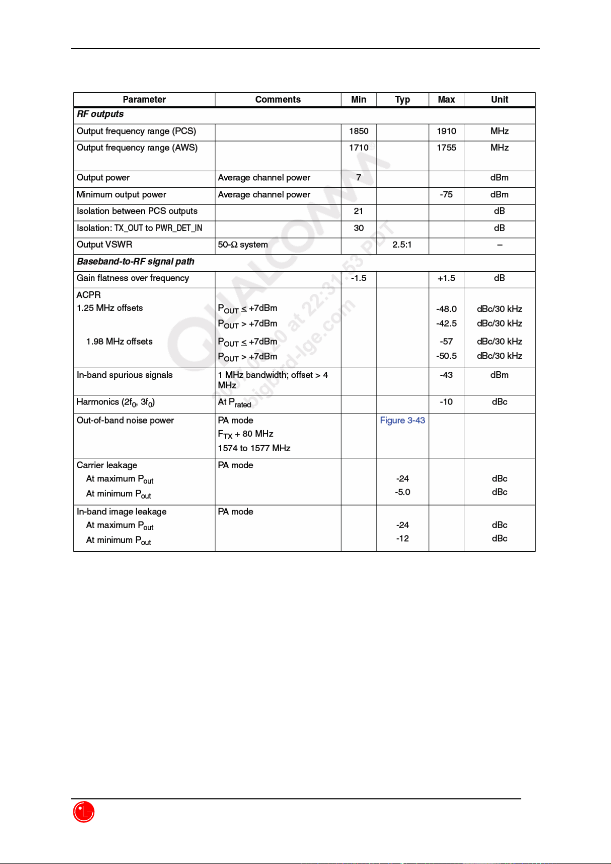
1) PCS: 0.240W
4.3.5 CDMA TX Frequency Deviation
1) PCS: ± 150Hz
4.3.6 CDMA TX Conducted Spurious Emissions
1) PCS : -42 dBc / 30KHz below
4.3.7 CDMA Minimum TX Power Control
1)
PCS : -50dBm below
12
LG-VM101
4.4 MS (Mobile Station) Transmitter Frequency
4.4.1 PCS mode
LG Electronics Inc.
Ch # Center Freq (MHz) Ch # Center Freq (MHz) Ch # Center Freq (MHz)
25
50
75
100
125
150
175
200
225
250
275
300
325
350
375
1851.25
1852.50
1853.75
1855.00
1856.25
1857.50
1858.75
1860.00
1861.25
1862.50
1863.75
1865.00
1866.25
1867.50
1868.75
425
450
475
500
525
550
575
600
625
650
675
700
725
750
775
1871.25
1872.50
1873.75
1875.00
1876.25
1877.50
1878.75
1880.00
1881.25
1882.50
1883.75
1885.00
1886.25
1887.50
1888.75
13
825
850
875
900
925
950
975
1000
1025
1050
1075
1100
1125
1150
1175
1891.25
1892.50
1893.75
1895.00
1896.25
1897.50
1898.75
1900.00
1901.25
1902.50
1903.75
1905.00
1906.25
1907.50
1908.75
LG-VM101
4.5 MS (Mobile Station) Receiver Frequency
Ch # Center Freq (MHz) Ch # Center Freq (MHz) Ch # Center Freq (MHz)
25
50
75
100
125
150
175
200
225
250
275
300
325
350
375
4.5.2 GPS mode : 1575.42MHz
4.5.1 PCS mode
LG Electronics Inc.
1931.25
1932.50
1933.75
1935.00
1936.25
1937.50
1938.75
1940.00
1941.25
1942.50
1943.75
1945.00
1946.25
1947.50
1948.75
425
450
475
500
525
550
575
600
625
650
675
700
725
750
775
1951.25
1952.50
1953.75
1955.00
1956.25
1957.50
1958.75
1960.00
1961.25
1962.50
1963.75
1965.00
1966.25
1967.50
1968.75
14
825
850
875
900
925
950
975
1000
1025
1050
1075
1100
1125
1150
1175
1971.25
1972.50
1973.75
1975.00
1976.25
1977.50
1978.75
1980.00
1981.25
1982.50
1983.75
1985.00
1986.25
1987.50
1988.75

LG-VM101
4.6 AC Adaptor
See Appendix
4.7 Cigar Lighter Charger
See Appendix
4.8 Hands-Free Kit
See Appendix
5.
Installation
5.1 Installing a Battery Pack
1) The Battery pack is keyed so it can only fit one way. Align the groove in the battery pack with the rail
on the back of the phone until the battery pack rests flush with the back of the phone.
2) Slide the battery pack forward until you hear a “click”, which locks the battery in place.
5.2 For Adapter Use
1) Plug the adapter into a wall outlet. The adapter can be operated from a 110V source.
When AC power is connected to the adapter.
2) Insert the adapter jack into the phone with the installed battery pack.
Red light indicates battery is being charged.. Green light indicates battry is fully charged.
5.3 For Mobile Mount
In order to reduce echo sound when using the Hands-Free Kit, make sure that the speaker and microphone are
not facing each other and keep microphone a generous distance from the speaker.
5.3.1 Installation Position
5.3.2 Cradle Installation
Choose an appropriate flat surface where the unit will not interface with driver’s movement or passenger’s
comfort. The driver/user should be able to access the phone with ease. Using the four self-tapping screws
provided, mount the supplied braket on the selected area. Then with the four machine screws provided, mount
the counterpart on the reverse side of the reverse side of the cradle. Secure the two brackets firmly together by
using the two bracket joint screws provide.
LG Electronics Inc.
15

LG-VM101
The distance between the cradle and the interface box must not exceed the length of the main cable.
5.3.3 Interface Box
Choose an appropriate flat surface ( somewhere under the dash on the passenger side is preferred ) and mount
the IB bracket with the four self-tapping screws provided. Clip the IB into the IB bracket.
Install the microphone either by cliiping I onto the sunvisor (driver’s side) or by attaching it to door post
(driver’s side), using a velcno adhesive tape (not included).
5.3.4. Microphone Installation
5.3.5 Cable Connections
Connect the red wire to the car battery positive terminal and the black wire to the car ground. Connect the green
5.3.5.1 Power and Ignition Cables
wire to the car ignition sensor terminal. ( In order to operate HFK please make sure to connect green wire to
ignition sensor terminal.) Connect the kit’s power cable connector to the interface box power receptacle.
5.3.5.2 Antenna Cable Connection
Connect the antenna coupler cable connector from the cradle to the external antenna connector. ( Antenna is not
included.)
LG Electronics Inc.
16
LG-VM101
Chapter 2. NAM Input Method
hapter 2. NAM Input Method
(Inputting of telephone numbers included)
NAM Programming Method and Telephone Number
Input
Method
PREPARATION
STEP ACTION
1
2
Press ##847446#.
Press 1~3 for NAM Programming (Service Prg.)
PROGRAMMING STEPS
ITEM Action
1 Activate Activate Phone Number through Telespree
2 View View Current MDN & MSID
3 Edit Activate Phone Number through editing MDN & MSID
4 Done Exit NAM Program menu
LG Electronics Inc.
17

LG-VM101
Chapter 3. Circuit Description
1.
RF Transmit/Receive Part
1.1 Overview
The Tx and Rx part employs the Direct Conversion system. The Tx and Rx frequencies are respectively
1850~1910MHz and 1930~1990MHz for PCS. The block diagram is shown in Page 71. RF signals received
through the antenna are seperated by quintplexer. RF Signal fed into the low noise amplifier (in QSC6055)
through the quintplexer. Then, they are combined with the signals of local oscillator (VCO) at the down
conversion mixer(in QSC6055) in order to create Base-band frequency. Then, this signal is changed into
digital signal by the analog to digital converter (ADC, A/D Converter), and the digital circuit part of the
QSC(Qualcomm Single Chip)6055 processes the data from ADC. The digital processing part is a demodulator.
In the case of transmission, RF Transmitter(in QSC6055) receives QPSK-modulated anlog signal from the
QSC6055. In QSC6055, the baseband quadrature signals are upconverted to PCS frequency bands and
amplified to provide signal drive capability to the power amp.
After that, the RF signal is amplified by the Power Amp in order to have enough power for radiation.
Finally, the RF signal is sent out to the cell site via the antenna after going through the coupler and quintplexer.
1.2 Description of Rx Part Circuit
1.2.1 Saw Filter (F1101)
The FSLF-S080HR is a Saw Filter that combines a US PCS band pass filter, and into a single, miniature package
with a single antenna port
The main function of Saw Filter is to prohibit the other band signals from flowing into the one band circuit
and
vice versa. The specification of LG-VM101 Saw Filter is described below:
.
LG Electronics Inc.
18
LG-VM101
The duplexer is a device using sharply tuned resonate circuits to isolate a transmitter from a receiver.
1.2.2 Duplexer
The main function of duplexer is to prohibit the rx band signals from flowing into the tx band circuit and vice
versa.
1.2.2.1 PCS Duplexer (DP1101)
The ACMD-7402 is a pcs duplexer of LG-VM101. The specification of LG-VM101 duplexer is
described below
The QSC6055 has cellular and PCS LNAs, respectively. The characteristics of Low Noise Amplifier (LNA)
1.2.3 LNAs (U2101)
are low noise figure, high gain, high intercept point and high reverse isolation.
The frequency selectivity characteristic of mobile phone is mostly determined by LNA.
The specification of LG-VM101 LNAs are described below:
LG Electronics Inc.
19
LG-VM101
1.2.3.1 PCS CDMA LNA performance specifications
LG Electronics Inc.
20
LG-VM101
1.2.4 GPS LNA (U1402)
The characteristics of Low Noise Amplifier (LNA) are low noise figure, high gain, high intercept point and high
reverse isolation. The frequency selectivity characteristic of mobile phone is mostly determined by LNA.
The specification of LG-AX300 GPS LNA is described below
The QSC6055 device performs signal down-conversion for PCS and GPS Dua l -band applications. It
1.2.5 Down-converter Mixers
contains all the circuitry (with the exception of external filters) needed to support conversion of received RF
signals to baseband signals. The three downconverting Mixers (PCS and GPS), and an LO Buffer Amplifier to
buffer the RF VCO to the RF Transmit Upconverter. The GPS LNA & mixers offer the most advanced and
integrated CDMA Rx solution designed to meet cascaded Noise Figure (NF) and Third-order Intercept Point
(IIP3) requirements of J-STD-018 specifications for Sensitivity, Two-Tone Intermodulation, and Single-tone
Desense.
Operation modes and band selection are specially controlled from the Qualcomm Single Chip QSC6055.
1.2.6 Rx RF SAW Filters (F1302)
The main function of Rx RF SAW filter is to attenuate mobile phone spurious frequency, attenuate direct RF
frequency pick up, attenuate noise at the image frequency originating in or amplified by the LNA and suppress
second harmonic originating in the LNA. The Rx RF SAW filter usually called image filter.
LG Electronics Inc.
21

LG-VM101
The circuit functions of the RF Receiver(in QSC6055) include Rx Automatic Gain Controller (AGC) with 90
dB dynamic range, quadrature RF mixers, down-conversion mixer from RF to base-band, low pass filters and
Analog to Digital Converters (ADC) for converting to digital base-band. The RFR includes clock generators that
drive the digital processor and a VCO which generates the LO frequency for base-band down-conversion.
Switching system is located in front of the RFR RX_IN_C_LB and RX_IN_C_HB terminal and is for PCS
band. The Rx AGC either amplifies or attenuates the received CDMA RF signal to provide a constant-
amplitude signal to the I/Q down-converter. The RF output of the Rx AGC amplifier separate into I-channel
and Q-channel base-band components and down-converted by mixer with quadrature LO. LO signals are
generated by a Voltage Controlled Oscillator (VCO) and frequency stabilized by external varactor-tuned
resonant tank circuit. The I/Q down converter outputs the CDMA signals at baseband frequency. Low-pass
filtering enables the receiver to select the desired baseband signals from the effects of unwanted noise or
adjacent-channel interference. I/Q base band components are converted to digital signals by two identical
4-bit ADCs.
1.2.7 RF Receiver (U2101)
1.3 Description of Transmit Part Circuit
The RF Transmitter(in QSC6055, base-band-to-RF Transmit Processor) performs all Tx signal-processing
functions required between digital base-band and the Power Amplifier Module (PAM). The base-band
quadrature signals are up-converted to the PCS frequency bands and amplified to provide signal drive
capability to the PAM. The RFT includes an RF mixer for upconverting analog baseband to RF, a programmable
PLL for generating Tx LO frequency, two PCS driver amplifiers and Tx power control through an 85 dB VGA.
As added benefit, the single sideband upconversion eliminates the need for a band pass filter normally required
between the upconverter and driver amplifier.
I, I/, Q and Q/ signals proceed from the QSC6055 are analog signal. In CDMA mode, These signals are
modulated by Quadrature Phase Shift King (QPSK). I and Q are 90 deg. out of phase, and I and I/ are 180 deg.
Tx IF signal can be obtained by mixing analog signal with 263.6(PCS) 1
generated by Tx VCO. The Tx IF signal is amplified by AGC controlled by QSC6055. The second mixer on
RFT converts IF signals into RF signals. After passing through the upconverter , RF signal is
Power Amplifier Module.
LG Electronics Inc.
1.3.1 RF Transmitter (U2101)
22
st
local osillator frequency which is
inputted into the
LG-VM101
1.3.1.1 PCS CDMA transmit signal path performance specifications
1.3.2 Power Amplifier (U1203)
The power amplifier that can be used in the PCS mode has linear amplification capability and high efficiency.
For higher efficiency, it is made up of one MMIC (Monolithic Microwave Integrated Circuit) for which RF input
terminal and internal interface circuit are integrated onto one IC after going through the AlGaAs/GaAs HBT
(heterojunction bipolar transistor) process. The module of power amplifier is made up of an output end interface
circuit including this MMIC. The maximum power that can be inputted through the input terminal is +10dBm
and conversion gain is about 28dB. RF transmit signals that have been amplified through the power amplifier
are sent to the duplexer.
LG Electronics Inc.
23

LG-VM101
1.4 Description of Frequency Synthesizer Circuit
The temperature variation of mobile phone can be compensated by TCXO. The reference frequency of a mobile
1.4.1 Voltage Control Temperature Compensation Crystal Oscillator
(VCTCXO, U1501)
phone is -30~+85 °C. The receives frequency tuning signals called TRK_LO_ADJ from QSC6055 as
0.5V~2.5V DC via R and C filter in order to generate the reference frequency of 19.2MHz and input it into the
frequency synthesizer of UHF band. Frequency stability depending on temperature is ±2.0 ppm.
2.
Digital/Voice Processing Part
2.1 Overview
The digital/voice processing part processes the user's commands and processes all the digital and voice signal
processing in order to operate in the phone. The digital/voice processing part is made up of a keypad/LCD,
receptacle part, voice processing part, modem part, memory part, and power supply part.
2.2 Configuration
This is used to transmit keypad signals to QSC6055. It is made up of a keypad backlight part that illuminates the
2.2.1 Keypad/LED and Receptacle Part
keypad, LCD part that displays the operation status onto the screen, and a receptacle that receives and sends out
voice and data with external sources.
The voice processing part is made up of an audio codec used to convert MIC signals into digital voice signals
and digital voice signals into analog voice signals, amplifying part for amplifying the voice signals and sending
them to the ear piece, amplifying part that amplifies ringer signals coming out from QSC6055, and amplifying
part that amplifies signals coming out from MIC and transferring them to the audio processor.
2.2.2 Voice Processing Part
QSC6055 (Qualcomm Single Chip) is the core elements of CDMA terminal and carries out the functions of
CPU, encoder, interleaver, deinterleaver, Viterbi decoder, Mod/Demod, and vocoder.
LG Electronics Inc.
2.2.3 QSC6055 Part
24

LG-VM101
2.2.4 Memory Part
The memory part is made up of a DDR SRAM/NAND memory.
2.2.5 Power Supply Part
The power supply part is made up of circuits for generating various types of power, used for the digital/voice
processing part.
2.3 Circuit Description
Once the keypad is pressed, the key signals are sent out to QSC6055 for processing. In addition, when the key is
pressed, the keypad lights up through the use of 2 Side View LEDs. The terminal status and operation are
displayed on the screen for the user with the characters and icons on the LCD.
2.3.1 Keypad/LCD and Receptacle Part
Moreover, it exchanges audio signals and data with external sources through the receptacle, and then receives
power from the battery or external batteries.
MIC signals are inputted into the audio codec(included in QSC6055) and converted into digital signals.
Oppositely, digital audio signals are converted into analog signals after going through the audio codec. These
signals are amplified at the audio amplifier and transmitted to the ear-piece. The signals from QSC6055 activate
the ringer by using signals generated in the timer in QSC6055.
2.3.2 Audio Processing Part
QSC6055 is the core element of CDMA system terminal that includes ARM926 EJS microprocessor core. It
supports both CDMA and GPS, operating in PCS spectrums. The subsystems within the QSC6055 include a
CDMA processor, a multi-standard Vocoder, an integrated CODEC with earpiece and microphone amplifiers,
general-purpose ADC for subsytem monitoring, an ARM926 EJS microprocessor, and both Universal Serial
Bus(USB) and an RS-232 serial interfaces supporting forward and reverse link data communications of 307.2
Kbps simultaneously. And it also contains complete digital modulation and demodulation systems for CDMA
standards.
2.3.3 MODEM Part
In QSC, coded symbols are interleaved in order to cope with multi-path fading. Each data channel is scrambled
by the long code PN sequence of the user in order to ensure the confidentiality of calls. Moreover, binary
quadrature codes are used based on walsh functions in order to discern each channel. Data created thus are
4-phase modulated by one pair of Pilot PN code and they are used to create I and Q data.
When received, I and Q data are demodulated into symbols by the demodulator, and then de-interleaved in
reverse to the case of transmission. Then, the errors of data received from viterbi decoder are detected and
corrected. They are voice-decoded at the vocoder in order to output digital voice data.
LG Electronics Inc.
25
LG-VM101
QSC6055
MIC1
Mic
MIC2
Ear-Mic
EAR1
Receiver
SPKR
OUT
[Figure 2-2] Block Diagram of Digital/Voice Processing Part
2.3.4 Memory Part
MCP contents 1 Gbits NAND flash memory and 512 Mbits DDR SRAM. In the Flash Memory part of MCP are
Speaker
programs used for terminal operation. The programs can be changed through down loading after the assembling
of terminals. On the SDRAM data generated during the terminal operation are stored temporarily.
When the battery voltage (+4.0V) is fed and the PWR key of keypad is pressed, the power-up circuitry in PM
(power management) circuit(in QSC6055) is activated by the PWR_ON_SW/ signal, and then the LDO
regulators embedded in PM circuit are operated and +1.3V_MSMC, +2.6V_MSMP, +1.8V_MSME and
+2.1V_MSMA are generated.
The Rx part (+2.1V_RFRX) and Tx part voltage (+2.1V_RFTX) are regulated by QSC6055
The logic part consists of internal CPU of QSC, RAM, MCP. The QSC6055 receives TCXO (=19.2MHz) from
U106 and controls the phone in both CDMA and GPS modes. The major components are as follows:
2.3.5 Power Supply Part
2.3.6 Logic Part
● CPU
The ARM926 EJS microprocessor includes a 3 stage pipelined RISC architecture, both 32-bit ARM and 16-bit
THUMB instruction sets, a 32-bit address bus, and a 32-bit internal data bus. It has a high performance and
low power consumption.
● MCP
Flash ROM is used to store the terminal’s program. Using the down-loading program, the program can be
changed even after the terminal is fully assembled.
SDRAM is used to store the internal flag information, call processing data, and timer data.
LG Electronics Inc.
26

LG-VM101
● KEYPAD
For key recognition, key matrix is setup using KYPD[0][1][2][3][4][9][11][13][15][17][19] signal from QSC.
2 Side view LEDs and backlight circuitry are included in the keypad for easy operation in the dark.
● LCD MODULE
LCD module contains a controller which will display the information onto the LCD by 16-bit data from the
QSC6055.
LG Electronics Inc.
27
LG -VM101
Chapter 4. Trouble Shooting
Chapter 4. Trouble Shooting
1. Rx Part Trouble
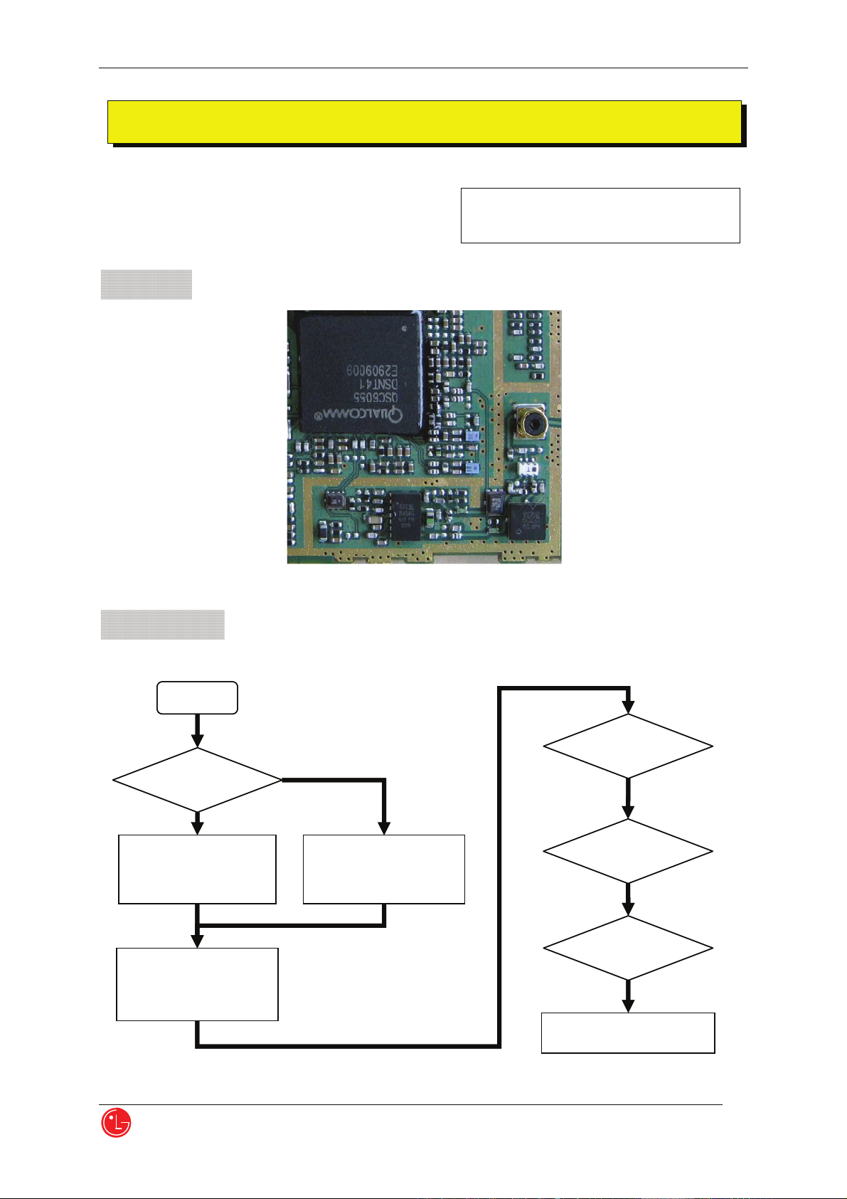
1.1 DCN & PCS Rx Trouble
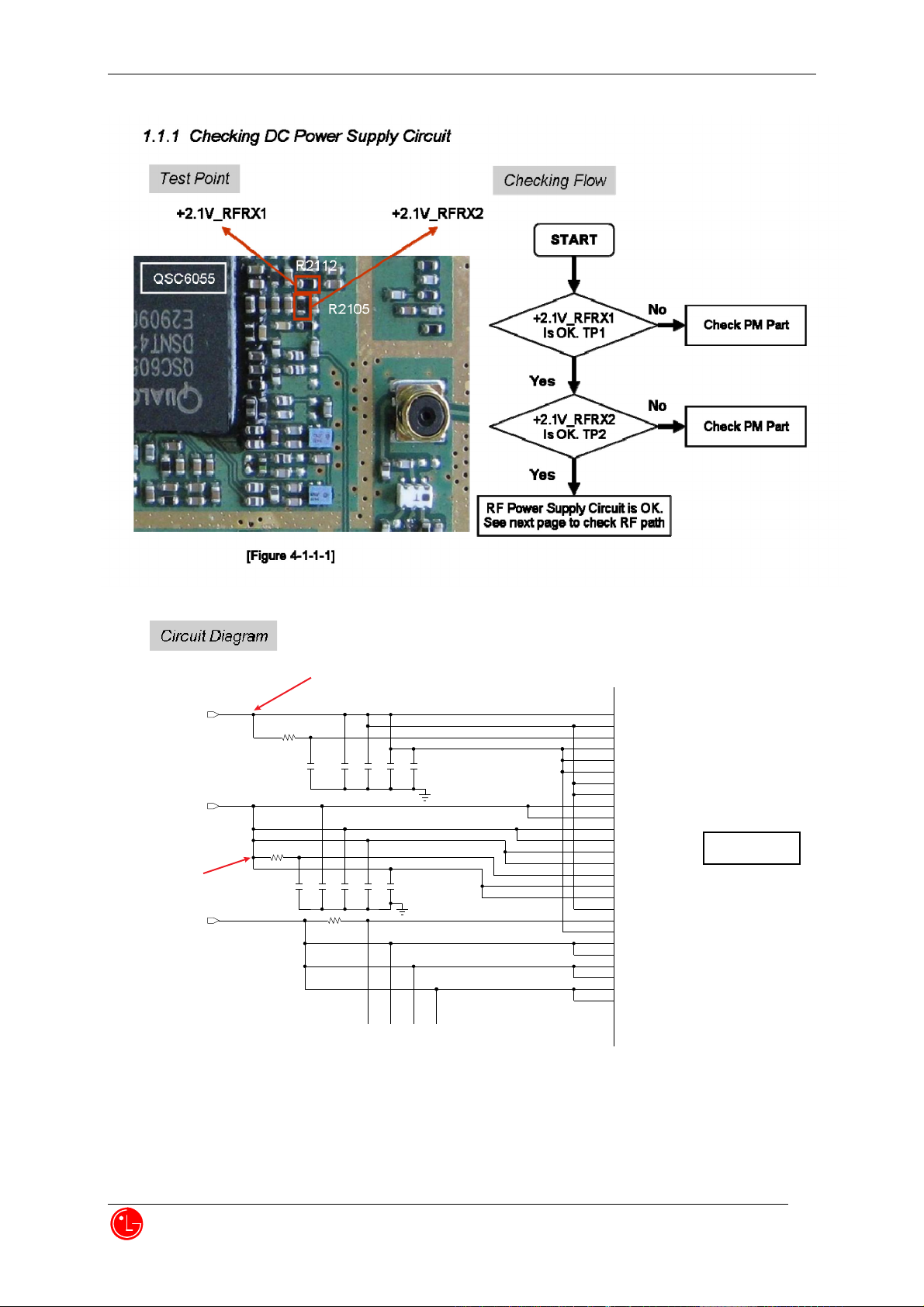
Test Point
Test Point
[Figure 4-1-1] DCN & PCS Rx Part
[Figure 4-1-1] DCN & PCS Rx Part
Note: This model supports PCS band.
Refer to PCS Part only.
Checking Flow
Checking Flow
START
START
PCS
PCS
DCN or PCS?
DCN or PCS?
DCN
DCN
Rx TEST SETUP(HHP)
Rx TEST SETUP(HHP)
- Test Channel : DCN 384
- Test Channel : DCN 384
- Test Band : US Cellular
- Test Band : US Cellular
- SID :18
- SID :18
Rx TEST SETUP(HHP)
Rx TEST SETUP(HHP)
- Sector Power : -30 dBm
- Sector Power : -30 dBm
Spectrum Analyzer Settiing
Spectrum Analyzer Settiing
Oscilloscope Setting
Oscilloscope Setting
Rx TEST SETUP(HHP)
Rx TEST SETUP(HHP)
- Test Channel : PCS 575
- Test Channel : PCS 575
- Test Band : US PCS
- Test Band : US PCS
- SID :18
- SID :18
1.1.1 Checking DC Power Supply Circuit
Check
Check
DC Power Supply
DC Power Supply
Circuit
Circuit
Check
Check
RX Signal Path
RX Signal Path
Check
Check
VCTCXO
VCTCXO
Redownload SW, CAL
Redownload SW, CAL
31 LG Electronics Inc.
28
LG-VM101
+2.1V _RFRX1
+2.1V _RFRX2
TP2
+2.1V _RFTX
R2112
R2105
4.7
2.2
1u
C2154
1u
C2121
R2107 10
TP1
1u
C2110
VDD_P 7_2
B21
VDD_R FRX1_1
C18
VDD_R FRX1_2
C20
VDD_R FRX1_3
C21
VDD_R FRX1_4
C22
VDD_R FRX1_5
E21
1u
1u
1u
1u
C2159
C2158
C2149
C2146
1u
1u
1u
C2132
C2150
C2141
F13
F21
A13
B13
C14
C15
C16
C17
E13
E15
F14
H16
H18
H22
J21
J23
K16
K18
K21
K22
AB17
VDD_R FRX1_6
VDD_R FRX1_7
VDD_R FRX1_8
VDD_R FRX2_1
VDD_R FRX2_2
VDD_R FRX2_3
VDD_R FRX2_4
VDD_R FRX2_5
VDD_R FRX2_6
VDD_R FRX2_7
VDD_R FRX2_8
VDD_R FRX2_9
VDD_R FTX_1
VDD_R FTX_2
VDD_R FTX_3
VDD_R FTX_4
VDD_R FTX_5
VDD_R FTX_6
VDD_R FTX_7
VDD_R FTX_8
VDD_R FTX_9
QSC6055
1.1.2 Checking Rx Signal Path
34 LG Electronics Inc.
29
 Loading...