

Page 1
SERVICE MANUAL MODEL : TCH-M1000 , TCH-M1000R
2005
DETACHABLE FRONT
PANEL CAR CD RECEIVER
SERVICE MANUAL
MODEL : TCH-M1000 , TCH-M1000R
CAUTION
BEFORE SERVICING THE UNIT, READ THE “SAFETY PRECAUTIONS”
IN THIS MANUAL.
Page 2

- 1-1 -
❍
SECTION 1. SUMMARY
• SERVICING PRECAUTIONS
..........................................................................................................
1-2
• ESD PRECAUTIONS
.......................................................................................................................
1-3
• SPECIFICATIONS
...........................................................................................................................
1-4
❍
SECTION 2. ELECTRICAL
• ELECTRICAL TROUBLESHOOTING GUIDE
.................................................................................
2-1
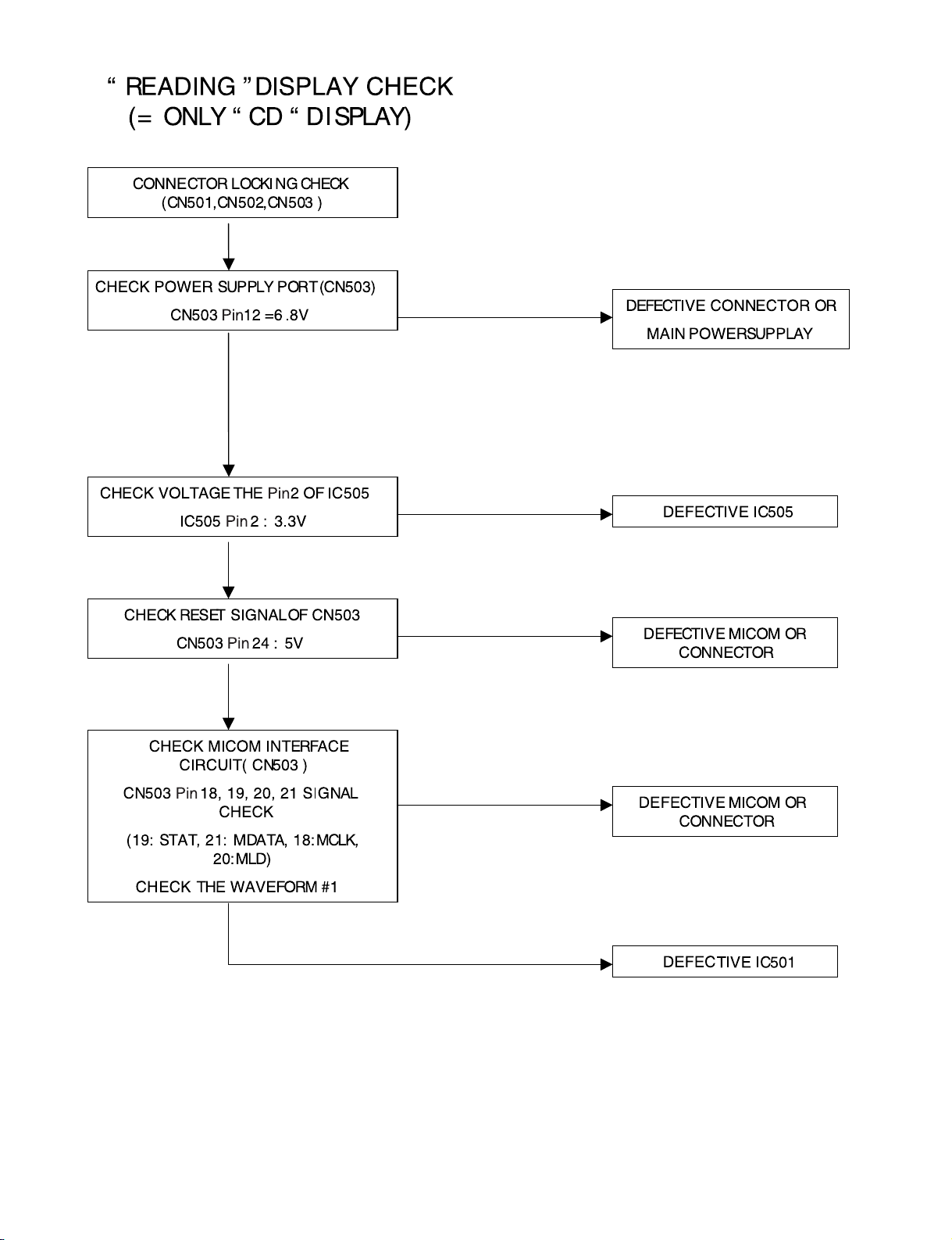
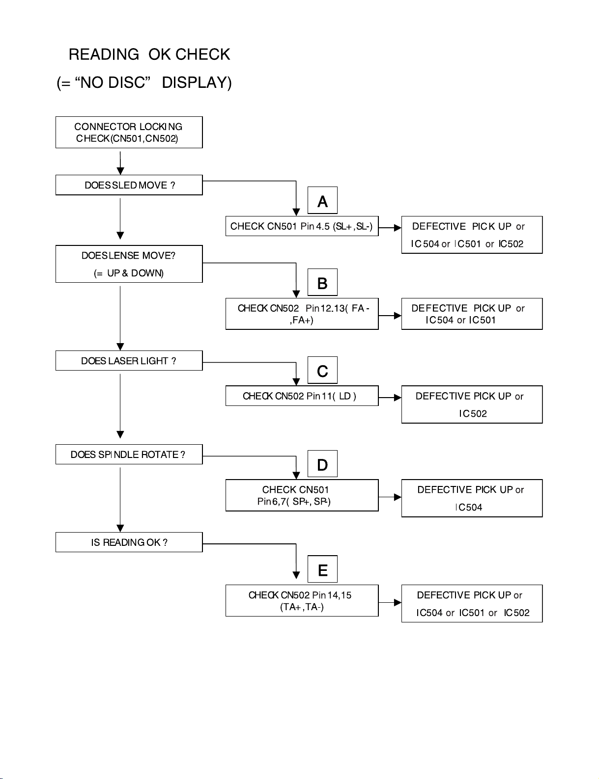
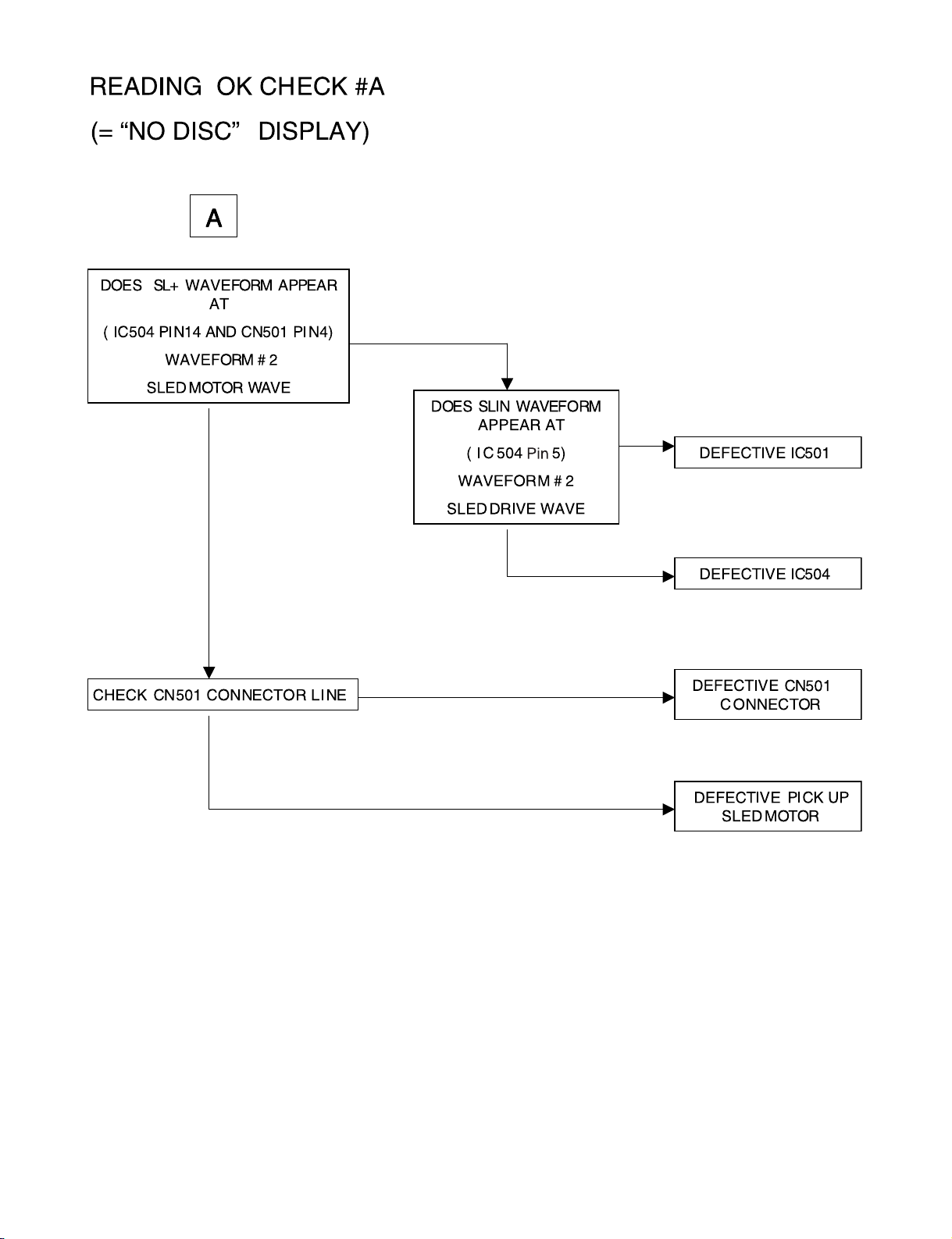
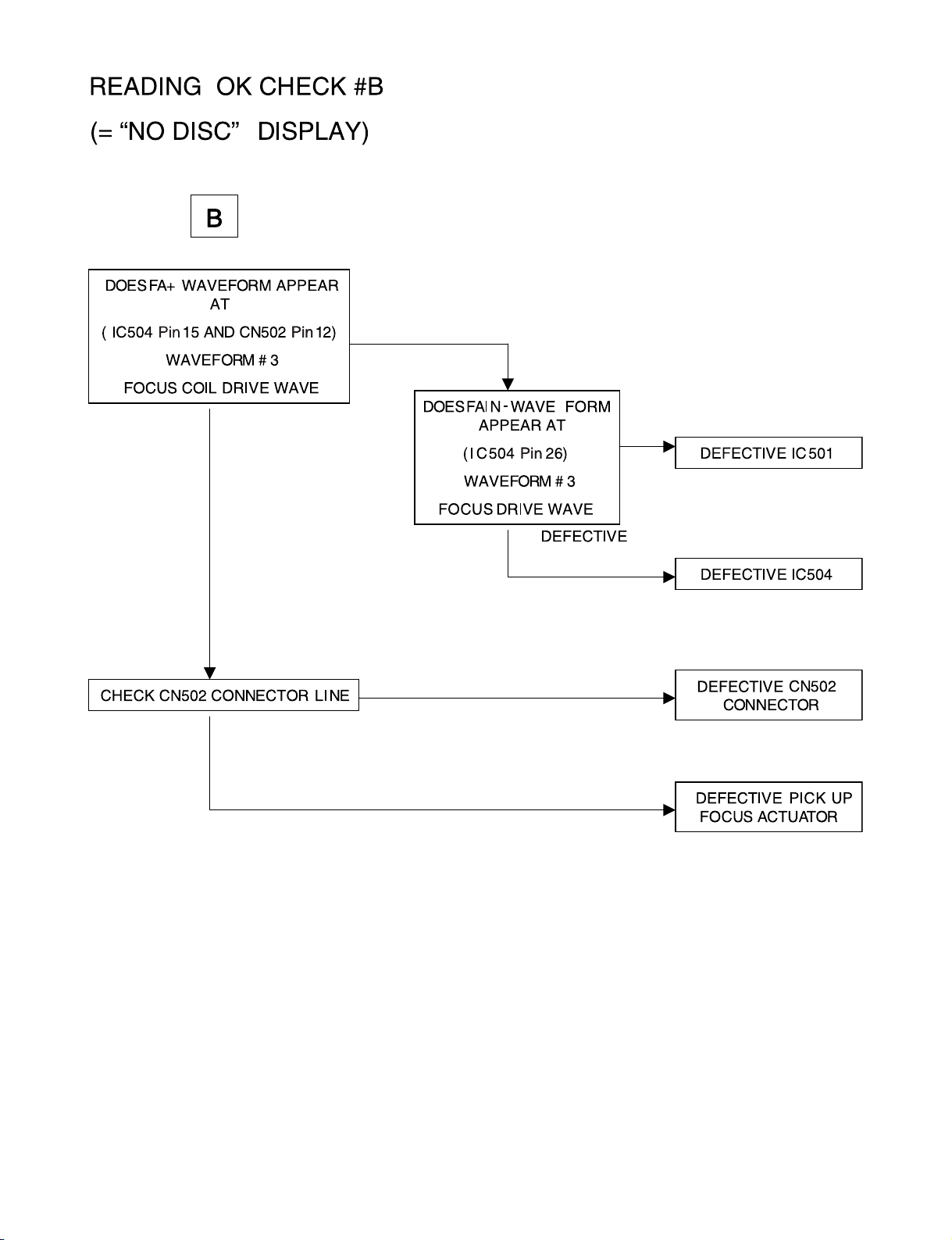
• CD PART TROUBLESHOOTING GUIDE
.........................................................................................
2-3
• WAVEFORMS OF MAJOR CHECK POINT
..................................................................................
2-11
• INTERNAL BLOCK DIAGRAM of ICs
............................................................................................
2-13
• BLOCK DIAGRAM
.........................................................................................................................
2-25
• SCHEMATIC DIAGRAM
................................................................................................................
2-27
• MAIN SCHEMATIC DIAGRAM
......................................................................................................
2-29
• CDP SCHEMATIC DIAGRAM
.......................................................................................................
2-31
• PRINTED CIRCUIT DIAGRAM
......................................................................................................
2-33
❍
SECTION 3. CABINET MAIN CHASSIS & MECHANISM
• EXPLODED VIEW
...........................................................................................................................
3-1
❍
SECTION 4. REPLACEMENT PARTS LIST
....................................................................
4-1
[CONTENTS]
Page 3

- 1-2 -
❏ SERVICING PRECAUTIONS
➊ Always disconnect the power source before:
1) Removing or reinstalling any component, circuit board, module or any other instrument assembly.
2) Disconnecting or reconnecting any instrument electrical plug or other electrical connection.
3) Connecting a test substitute in parallel with an electrolytic capacitor in the instrument.
CAUTION: A wrong part substitution or incorrect polarity installation of electrolytic capacitors may result in
an explosion hazard.
➋ Do not defeat any plug/socket B+ voltage interlocks with which instruments covered by this service
manual might be equipped.
❸ Do not apply power to this instrument and or any of its electrical assemblies unless all solid-state
device heat sinks are correctly installed.
❹ Always connect a test instrument’s ground lead to the instrument chassis ground before
connecting the test instrument positive lead. Always remove the test instrument ground lead last.
1) The service precautions are indicated or printed on the cabinet, chassis or components. When servicing,
follow the printed or indicated service precautions and service materials.
2) The Components used in the unit have a specified conflammability and dielectric strength. When
replacing any components, use components which have the same ratings. Components marked in
the circuit diagram are important for safety or for the characteristics of the unit. Always replace with the
exact components.
3) An insulation tube or tape is sometimes used and some components are raised above the printed writing
board for safety. The internal wiring is sometimes clamped to prevent contact with heating components.
Install them as they were.
4) After servicing always check that the removed screws, components and wiring have been installed
correctly and that the portion around the service part has not been damaged. Further check the insulation
between the blades of attachment plug and accessible conductive parts.
SECTION 1. SUMMARY
Page 4
- 1-3 -
❏
ESD PRECAUTIONS
[Electrostatically Sensitive Devices (ESD)]
Some semiconductor (solid state) devices can be damaged easily by static electricity. Such omponents
commonly are called Electrostatically Sensitive Devices (ESD). Examples of typical ESD devices are
integrated circuits and some field-effect transistors and semiconductor chip components. The following
techniques should be used to help reduce the incidence of component damage caused by static electricity.
1) Immediately before handling any semiconductor component or semiconductor-equipped assembly, drain
off any electrostatic charge on your body by touching a known earth ground. Alternatively, obtain and
wear a commercially available discharging wrist strap device, which should be removed for potential
shock reasons prior to applying power to the unit under test.
2) After removing an electrical assembly equipped with ESD devices, place the assembly on a conductive
surface such as aluminum foil, to prevent electrostatic charge buildup or exposure of the assembly.
3) Use only a grounded-tip soldering iron to solder or unsolder ESD devices.
4) Use only an anti-static solder removal device. Some solder removal devices not classified as “anti-static”
can generate electrical charges sufficient to damage ESD devices.
5) Do not use freon-propelled chemicals. These can generate electrical charges sufficient to damage ESD
devices.
6) Do not remove a replacement ESD device from its protective package until immediately before you are
ready to install it. (Most replacement ESD devices are packaged with leads electrically shorted together
by conductive foam, aluminum foil or comparable conductive material).
7) Immediately before removing the protective material from the leads of a replacement ESD device, touch
the protective material to the chassis or circuit assembly into which the device will be installed.
CAUTION: Be sure no power is applied to the chassis or circuit, and observe all other safety precautions.
8) Minimize bodily motions when handling unpackaged replacement ESD devices. (Otherwise harmless
motion such as the brushing together of your clothes fabric or the lifting of your foot from a carpeted floor
can generate static electricity sufficient to damage an ESD device).
[CAUTION. GRAPHIC SYMBOLS]
THE LIGHTNING FLASH WITH APROWHEAD SYMBOL. WITHIN AN EQUILATERAL
TRIANGLE, IS INTENDED TO ALERT THE SERVICE PERSONNEL TO THE PRESENCE
OF UNINSULATED “DANGEROUS VOLTAGE” THAT MAY BE OF SUFFICIENT
MAGNITUDE TO CONSTITUTE A RISK OF ELECTRIC SHOCK.
THE EXCLAMATION POINT WITHIN AN EQUILATERAL TRIANGLE IS INTENDED TO
ALERT THE SERVICE PERSONNEL TO THE PRESENCE OF IMPORTANT SAFETY
INFORMATION IN SERVICE LITERATURE.
Page 5

- 1-4 -
1. GENERAL
Power requirements
.....................................................................................................................
DC12V~15V
Ground system
...................................................................................................................................
Negative
Dimensions(W x H x D)
......................................................................................................
188 x 58 x 166mm
Weight
..............................................................................................................................................
Net: 1.3kg
2. RADIO SECTION
FM AM(MW)
Frequency range 65.0~74.0MHz(Optional), 522~1,620kHz
87.5~108MHz (Optional:530~1,710kHz/ 520~1,620kHz)
Intermediate frequency 10.8MHz 450kHz
Usable sensitivity 10dBµV 28dBµV
Signal to noise ratio 55dB 45dB
3. COMPACT DISC SECTION
Frequency response
.....................................................................................................................
40Hz~20kHz
Channel separation
......................................................................................................................
50dB(1kHz)
Signal to noise ratio ..................................................................................................................................
60dB
4. AUDIO SECTION
Maximum output power
.......................................................................................................................
50W x 4
Speaker impedance
...............................................................................................................
4Ω x 4 or 8Ω x 4
NOTE: The design and specifications are subject to change without notice in the sourse of product
improvement.
❏
SPECIFICATIONS
Page 6

- 2-1 -
SECTION 2. ELECTRICAL
❏ ELECTRICAL TROUBLESHOOTING GUIDE
Any Key power on.
Is power turnd on?
DISC loading?
Does initial reading occur?
Can disc be played?
Is audio output supplied?
Check power supply circuitry.
Q260, Q380, Q381, IC401 Pin3
IC201 Pin2
Check loading supply circuitry.
Q350,Q351,PN505, IC401 Pin1
Check laser circuitry.
Q501, IC502
Check focusing circuitry.
Q501,IC502
Check DISC.
Check tracking servo circuitry.
Q501,IC502
Check audio circuitry.
IC502,IC601,IC801
OK
YES
YES
YES
YES
YES
YES
NO
NO
NO
NO
NO
(1) No Power.
Page 7
- 2-2 -
YES
YES
YES
YES
YES
YES
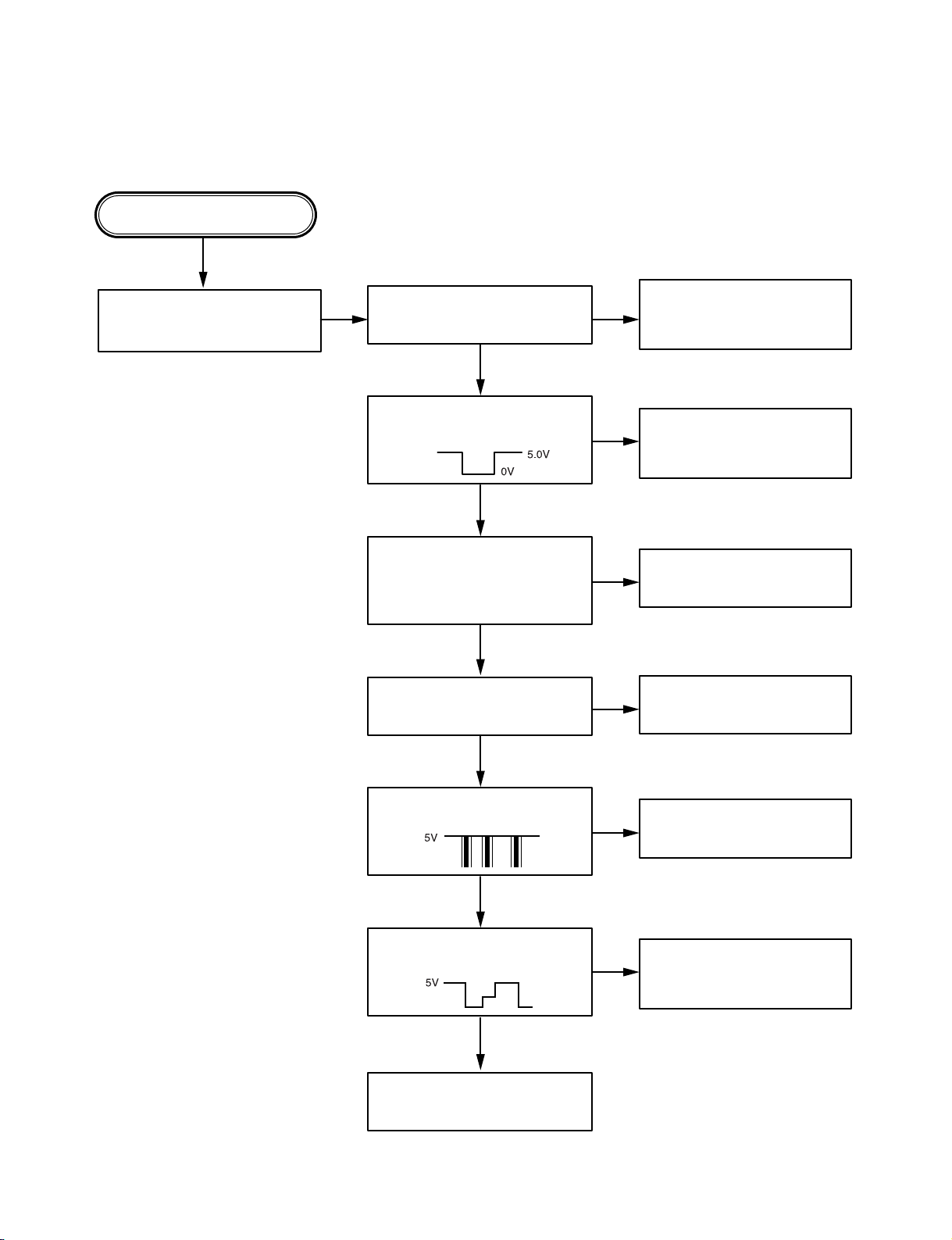
(2) LCD light abnornal.
Any Key power on.
(without DISC)
Do display LCD then light?
Check voltage in the power
supply circuitry.
Power supply circuitry
defective.
Q380,Q381,IC403
Reset circuit defective.
IC201 Surrounding circuit
defective.
X401, C413,C414 defective.
Q260, PN401 front PCB
pattern defective.
IC401, Pin66, 67, 88, 89 front
PCB pattern defective.
IC901, Surrounding circuit
PCB pattern defective.
Is u-com IC401 reset circuit
normal? Pin10
Is u-com IC401 keyin Pin 9, 37
5volt input?
Is u-com IC401 Pin 66,67,88,89
output waveform normal?
Is IC901 Com1, Com2, Com3
output waveform normal?
Display LCD connector defective.
Is u-com IC401X1, X2 terminal
Pin38, 39 input?
OSC : 9.8304MHz
NO
NO
NO
NO
NO
NO
NO
Page 8
- 2-3 -
Page 9
- 2-4 -
Page 10
- 2-5 -
Page 11
- 2-6 -
Page 12
- 2-7 -
Page 13

- 2-8 -
Page 14

- 2-9 -
Page 15

- 2-10 -
Page 16

- 2-11 -
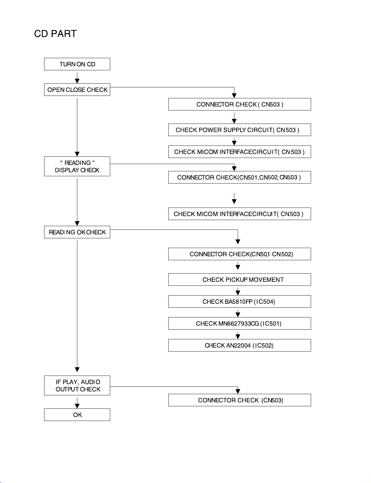
❏ WAVEFORMS OF MAJOR CHECK POINT
#1. MICOM INTERFACE WAVEFORM
(CN503 1 9,2 1 ,1 8,20) during normal play
#2. SLED DRIVE AND MOTOR WAVEFORM
(IC504 pin5, 1 4) when focus search
#3. FOCUS DRIVE AND MOTOR WAVEFORM
(R5 1 3, IC504 pin 1 5)
• When focus search failed or there is no disc on the
tray
• There is disc on tray and focus search success
Page 17

- 2-12 -
#4. SPINDLE DRIVE AND MOTOR WAVEFORM
(IC504 pin6, 1 2) when TOC reading
#5. TRACK DRIVE AND MOTOR WAVEFORM
(R508, IC504 pin23) during normal play
#6. RF, TRACKING AND FOCUS ERROR WAVEFORM
(IC502 pin8, 2 1 , 23) during normal play
Page 18

- 2-13 -
■ IC401 LC875465B
1) PORT ASSIGNMENT
❏
INTERNAL BLOCK DIAGRAM of ICs
Page 19

- 2-14 -
2) PORT DESCRIPTION
Page 20

- 2-15 -
Pin I/O
26
I
27
O
28 O
29 O
30
O
31
I
32
O
33 O
34 O
35 I
36 O
37 O
38 O
39 I
40 O
41 I
42 O
43 O
44 45 46 O
47 O
48 O
49 O
50 O
51 O
52 O
53 O
54 I
55 O
56 I
57 I
58 I
59 I
60 O
61 O
62 O
63 I
64 I
65 I
66 O
67 I
68 O
69 I
70 71 72 I
P34
P33
PCD_MUTE
CD s audio signal mute output
PDSP_ODA
In MD, motor drive rs power save command ouput
Power Save Mode(High), N ormal Mode(Low)
In MD, all motors output "cut off" command ouput
Cut Off Mode(High), Normal Mode(Low)
Constant velocit y signal input
Ok(High), Not Ok(Low)
DSP chip enable output
In MD, load motor "forward" command output
To DSP, data output
From DSP, data input
Clock output for interface with DSP
In MD, SW2 state input. Refer to CD Player.
DSP power suppler ON ouptut
Description
Beep sound (2KHz) output
To LCD driver, data output
Not to be used
Clock output for interface with LCD driver
Not to be used
Not to be used
Not to be used
Power supply (+5V)
Ground
PLL IC enable output
LCD driver enabl e output
LCD driver r e set output
Normal(High), Reset(Low)
External amplifier ON output
LED flashing control output
Not to be used
Not to be used
Not to be used
Focusing OK signal input
Ok(High), Not Ok(Low)
DSP reset output
Not to be used
Not to be used
Not to be used
Not to be used
To CD changer, data output
For diode option check, s ignal 1 output. Refer to Option Diode.
For diode option check, s ignal 2 output. Refer to Option Diode.
For diode option check, s ignal 1 or 2 input2. Refer to Option Diode.
For diode option check, s ignal 1 or 2 input1. Refer to Option Diode.
For diode option check, s ignal 1 or 2 input0. Refer to Option Diode.
Clock output for interface with PLL IC
From PLL IC, data input
To PLL IC, data output
Telephone mute input
Ground
Power supply (+5V)
Not to be used
P32
PCD_FWD
Name in ModelName in Micom
PCD_SW2P31
PCD_PWR
P10/SO0
PDSP_IDAP11/SI0/SB0
PDSP_OCLKP12/SCK0
PDRV_OPSP13/SO1
PDRV_OMUTEP14/SI1/SB1
PDSP_IFSEQP15/SCK1
PDSP_OCENP16/T1PWML
PBEEP
PFRT_DOSI2P0/SO2
N.CSI2P1/SI2/SB2
PFRT_CLKSI2P2/SCK2
N.CSI2P3/SCK20
N.CPWM1
N.CPWM0
VDDVDD2
GNDVSS2
PPLL_CEP00
PFRT_CEP01
PFRT_RESP02
PREMOTEP03
PLEDP04
N.CP05
N.CP06
N.CP07
PDSP_IDRFP20/INT4/T1IN
PDSP_IRSTP21/INT4/T1IN
N.CP22/INT4/T1IN
N.CP23/INT4/T1IN
N.CP24/INT5/T1IN
N.CP25/INT5/T1IN
PCDC_DOP26/INT5/T1IN
POPT_OUT0P27/INT5/T1IN
POPT_OUT1PB7/D7
POPT_IN2PB6/D6
POPT_IN1PB5/D5
POPT_IN0PB4/D4
PPLL_CLKPB3/D3
PPLL_DIPB2/D2
PPLL_DOPB1/D1
PTEL_MUTEPB0/D0
GNDVSS3
VDDVDD3
N.CPC7/A7
F
LowH
B
H
H
R
H
L
O
LowL
F
P
P
’
’
’
CD_F
ow
ow
igh
igh
CD_R
igh
igh
unction
pen mode
everse
orward
reak mode
P17/T1PWMH/BUZ
Page 21

- 2-16 -
■ IC501 MN6627933
1) PORT ASSIGNMENT
Pin I /O
73 O
74 O
75
O
76 O
77 I
78 I
79 O
80 I
PC0/A0
PA0/CS2#
PC4/A4
PC3/A3
PC2/A2
PC1/A1
PFRT_DET
Fr ont Pannel Ok(High) , Absent(Low)
Clock for interface wi th vol ume controll er
System Power supplier ON output
On(High), Off(Low)
Description
To volume contr oller, data out put
To power amp, "M UTE" command output
Mute(Hi gh), Sound(Low)
Name in Micom
PPWR_MU TEPC6/A6
PEV_CLKPC5/A5
PPWR
Name i n M odel
PEV_DO
Fr om ISO jack, ACC signal i nput
ACC On(Low), ACC Off(Hi gh)
Not to be used
CD changer power suppl ier ON output
CDC On(High), CDC Off(Low)
PACC
N.C
PCDC_PWR
Fr ont pannel existence signal input
Page 22

- 2-17 -
2) Block Diagram
Page 23

- 2-18 -
3) PORT DESCRIPTION
Pin No. Symbol I/O Function
1 D11 I/O DRAM data signal I/O 11
2 D10 I/O DRAM data signal I/O 10
3 D9 I/O DRAM data signal I/O 9
4 D8 I/O DRAM data signal I/O 8
5 UDQM O SDRAM upper byte data mask signal output
6 SDRCK O SDRAM clock signal output
7 A11 O DRAM address signal output 11
8 A9 O DRAM address signal output 9
9 A8 O DRAM address signal output 8
10 A7 O DRAM address signal output 7
11 A6 O DRAM address signal output 6
12 A5 O DRAM address signal output 5
13 A4 O DRAM address signal output 4
14 LDQM O SDRAM lower byte data mask signal output
15 NWE O DRAM write enable signal output
16 NCAS O DRAM CAS control signal output
17 NRAS O DRAM RAS control signal output
18 NCS O SDRAM chip select signal output
19 A3 O DRAM address signal output 3
20 A2 O DRAM address signal output 2
21 A1 O DRAM address signal output 1
22 A0 O DRAM address signal output 0
23 DRVDD1 I Power supply 1 for DRAM interface I/O
24 DVSS1 I Ground 1 for digital circuits
25 A10 O DRAM address signal output 10
26 *BA1 O SDRAM bank selection signal output 1
27 *BA0 O SDRAM bank selection signal output 0
28 DVDD1 I Power supply 1 for internal digital circuits
29 SPOUT O Spindle drive signal output (absolute value)
30 *SPPOL O Spindle drive signal output (polarity)
31 TRVP O Traverse drive signal output (positive polarity)
32 *TRVM O Traverse drive signal output (negative polarity)
33 *TRVP2 O Traverse drive signal output 2 (positive polarity)
34 *TRVM2 O Traverse drive signal output 2 (negative polarity)
35 TRP O Tracking drive signal output (positive polarity)
36 *TRM O Tracking drive signal output (negative polarity)
37 FOP O Focus drive signal output (positive polarity)
38 *FOM O Focus drive signal output (negative polarity)
39 IOVDD1 I Power supply 1 for digital I/O
40 TBAL O Tracking balance adjustment signal output
41 FBAL O Focus balance adjustment signal output
42 FE I Focus error signal input
43 TE I Tracking error signal input
44 ADPVCC I Voltage input for supply voltage monitor
45 RFENV I RF envelope signal input
46 LDON O Laser ON signal output
47 NRFDET I RF detectoion signal input
48 OFT I Off-track signal input
49 BDO I Dropout signal input
50 AVDD1 I Power supply 1 for analog circuits
51 IREF I Analog reference current input
52 ARF I RF signal input
53 DSLF O DSL loop filter pin
54 PWMSEL I PWM output mode selection input Low: Direct High: 3-state
55 PLLF O PLL loop filter pin (for phase comparison)
56 PLLFO O PLL loop filter pin (for speed comparison)
57 AVSS1 I Ground 1 for analog circuits
58 LOOUTL O L-ch audio output for line-out output
59 LOVSS1 I Ground for line-out output
Page 24

- 2-19 -
Pin No. Symbol I/O Function
60 LOOUTR O R-ch audio output for line-out output
61 LOVDD1 I Power supply for line-out output
62 N.C. - 63 TMON1 O Test monitor output 1
64 N.C. - 65 N.C. - 66 TMON2 O Test monitor output 2
67 DVDD3 I Power supply 3 for digital circuits
68 DVSS2 I Ground 2 for digital circuits
69 *EXT0 I/O Expansion I/O port 0
70 *EXT1 I/O Expansion I/O port 1
71 *EXT2 I/O Expansion I/O port 2
72 MCLK I Microcontroller command clock signal input
73 MDATA I Microcontroller command data signal input
74 MLD I Microcontroller command load signal input
75 *STAT O Status signal output
76 *BLKCK O Subcode block clock signal output
77 *SMCK O 4.2336-/8.4672-MHz clock signal output
78 *PMCK O 88.2-kHz clock signal output
79 *TX O Digital audio interface signal output
80 *FLAG O Flag signal output
81 NRST I LSI reset signal input
82 NTEST I Test mode setting input
83 DVSS3 I Ground 3 for digital circuits
84 X1 I Crystal oscillator circuit input
85 X2 O Crystal oscillator circuit output
86 IOVDD2 I Power supply 2 for digital I/O
87 DVDD2 I Power supply 2 for internal digital circuits
88 D2 I/O DRAM data signal I/O 2
89 D1 I/O DRAM data signal I/O 1
90 D0 I/O DRAM data signal I/O 0
91 D3 I/O DRAM data signal I/O 3
92 D4 I/O DRAM data signal I/O 4
93 D5 I/O DRAM data signal I/O 5
94 D6 I/O DRAM data signal I/O 6
95 D7 I/O DRAM data signal I/O 7
96 D15 I/O DRAM data signal I/O 15
97 D14 I/O DRAM data signal I/O 14
98 DRVDD2 I Power supply 2 for DRAM interface I/O
99 D13 I/O DRAM data signal I/O 13
100 D12 I/O DRAM data signal I/O 12
Page 25

- 2-20 -
■ IC503 M12L16161A
1) PORT ASSIGNMENT
2) BLOCK DIAGRAM
CLK
ADD
LCKE
LRAS
LCBR LWE
CLK
CKE
CS RAS CAS
WE L(U)DQM
LDQM
LWCBR
LCAS
Bank Select
LWE
LDQM
DQI
Data Input Regidter
512K x 16
512K x 16
Column Decoder
Latency & Burst Length
Programming Register
Timing Register
Address Register
Row Decoder
LCBR
LRAS
Sense AMP
I/O Control
Output Buffer
Col. Buffer
Row Buffer
Refresh Counter
Page 26

- 2-21 -
Pin Name Input Function
CLK System Clock Active on the positive going edge to sample all inputs.
CS Chip Select
Disables or enables device operation by masking or enabling all inputs except
CLK, CKE and L(U)DQM.
Masks system clock to freeze operation from the next clock cycle. CKE
CKE Clock Enable should be enabled at least one cycle prior to new command. Disable input
buffers for power down in standby.
A0~A10/AP Address
Row/Column addresses are multiplexed on the same pins. Row address:
RA0~RA10, column address: CA0~CA7
BA Bank Select Address
Selects bank to be activated during row address latch time. Selects bank for
read/write during column address latch time.
RAS Row Address Strobe
Latches row addresses on the positive going edge of the CLK with RAS low.
Enables row access & precharge.
CAS Column Address Strobe
Latches column addresses on the positive going edge of the CLK with CAS
low. Enables column access.
WE Write Enable
Enables write operation and row precharge. Latches data in starting from
CAS, WE active.
L(U)DQM Data Input / Output Mask
Makes data output Hi-Z, tSHZ after the clock and masks the output. Blocks
data input when L(U)DQM active.
DQ0~15 Data Input / Output Data inputs/outputs are multiplexed on the same pins.
VDD/VSS Power Supply/Ground Power and ground for the input buffers and the core logic.
VDDQ/VSSQ Data Output Power/Ground
Isolated power supply and ground for the output buffers to provide improved
noise immunity.
N.C/RFU No Connection/ This is recommended to be left No Connection on the
Reserved for Future Use device.
■ PIN Function table
■ IC504 BA5810FM
28
27
26
25 24
23
22
21 20 19 18 17 16 15
1234 5
6
7 8 9 1011121314
++— + —
+ —
+ —
+ —
7.5k
7.5k
7.5k
7.5k
LOADING PRE
FWE REV
X3
POWER
SAVE
16k
16k
16k
16k
PREVCC
(PRE. LODING)
PREVCC12
(CH1. CH2)
CD1~
CB4
MUTE
POWVCC34
(CH3, CH4)
10k
10k
10k 10k
10k
10k
10k
10k
LEVEL
SHIFT
LEVEL
SHIFT
LEVEL
SHIFT
LEVEL
SHIFT
10k
10k
10k
10k
10k
10k
Page 27

- 2-22 -
■ IC505 AMC1117
■ BLOCK DIAGRAM
Page 28

- 2-23 -
■ IC601 PT2313L
RB
RB
TREB_RBIN_RBOUT_RLOUDRINROUTREFAGNDVDD
RIN1
RIN1
RIN2
RIN2
RIN3
RIN3
LIN3
LIN3
Input
Selector
& Gain
Control
LIN2
LIN2
LIN1
LOUT LIN LOUD_L BOUT_L BIN_L TREB_L
LFOUT
Mute
Mute
Mute
Mute
Speaker
ATT
Speaker
ATT
Speaker
ATT
Speaker
ATT
LROUT
CLK
DATA
DGND
RFOUT
RROUT
LIN1
2
11
10
9
13
14
15
17 16 12 19
18
4
25
23
28
27
26
24
22
31 7 6 8 21
20
5
Supply
Bass
Serial Bus Decoder & Latches
Bass
Treble
Treble
Voume
&
Loudness
Voume &
Loudness
Page 29

- 2-24 -
■ IC801 TDA8571J
+
-
+
-
+
-
+
-
+
-
+
-
+
-
+
-
PGND1 PGND2 PGND3 PGND4
MGG153
OUT4
-
OUT4+
OUT3+
DIAGNOSTIC
OUT2+
V
OUT1+
OUT3
-
OUT2
-
OUT1
-
21
20
22
19
17
9
5
7
4
2
23 16
10
11
12
13
14
30 K¥
30 K¥
30 K¥
30 K¥
IN1
MODE
IN2
SGND
IN3
IN4
8 1 15
186
3
ref
V
P1
V
P2
V
P3
V
P4
V
ref
V
DIAG
■ IC901 LC75811
Page 30

2-25 2-26
❏ BLOCK DIAGRAM
TU101
CET85XX
16,17,
18,19
24,25
10,14
6
13,19
7
11,12
2(LR)
20
4,14
OP AMP
S4560
LINE SW/E.VOLUME
27
28
2
9.4V REG
Q360,ZD361
22,23
10,14
CCNTROL
Q720,721,722,723
2(RL,RR)
2(FL,FR)
2(RL,FR)
MUTE
POWER AMP
TA8275H
11,14
12,15
22
4-CH
(FL,FR,RL,RR)
2, 8, 18, 24
7,9
21,23
17,19
3, 5
L-SPEAKER
FRONT
R-SPEAKER
L-SPEAKER
REAR
R-SPEAKER
LINE-OUT
(OPTION)
CDC SIGNAL
9.4V
RADIO VCC
Q350,ZD313
POWER 5V
Q282,Q283
14V
POWER ON
Q380,381
ANT CONTROL
Q390,391
REMOTE
CONTROL
Q320,321
PN801 #16
BACK_UP
PN801 #10
PWR_ANT
PN801 #6
REMOTE
PICK-UP
CD MECHA
(4404R-C004A)
DSP IC
(MN6627933)
29, 31, 35, 37
5,6,23,26 15,16,17,18
9,10,11,
12,13,14
MOTOR
DRIVE IC
(BA5810FM)
4
58, 60
7,8,20
1,2
RF IC
AN22004A
72, 73, 74,
75, 76, 81
3.3V REG
IC805
24
RESET
IC201
5V CONVERT
Q260, ZD261, D201
REG 10V
IC403
ACC DETECTOR
Q230,D231,D232
PHONE MUTE
Q280,281
PN801 #14
ACC
PN801 #5
PHONE
PN801 #11
DIMMER
7.5V REG
Q310,Q351
32
71,69,68,70
73,74,75,33,34,7
14, 19
29
15, 16, 17, 18
2
10
55
24
11
U-COM
uPD789166
41 42
3 90 5 91 4
43
56, 57
66, 67
88, 89
39
38
KEY MATRIX
RESISTOR
RADER
9.8304MHz
LCD DRIVER
LC75811W
77~80
69~72
1~50
LCD DISPLAY
32.768
Page 31

❏ MAIN SCHEMATIC DIAGRAM
2-27 2-28
Page 32

2-29 2-30
❏ FRONT SCHEMATIC DIAGRAM
Page 33

2-31 2-32
❏ CDP SCHEMATIC DIAGRAM
Page 34

2-33 2-34
❏ PRINTED CIRCUIT DIAGRAM
1. LED P.C.BOARD
(COMPONENT SIDE)
2. FRONT P.C. BOARD
(COMPONENT SIDE)
Page 35

2-35 2-36
3. MAIN P.C. BOARD
(SOLDER SIDE)
Page 36

2-37 2-38
4. CDP P.C. BOARD(COMPONENT SIDE)
Page 37

2-39 2-40
Page 38

3-1 3-2
■ EXPLODED VIEW
A40
281
452
282
452
453
450
301
A47
452
286
A26
287
452
283
284
452
A46
454
270
A45
275
277
454
273
276
278
271
272
268
330
451
267
266
A43
265
263
264
256
255
253
269
250
252
262
251
A41
257
258
259
260
261
254
CAUTION
Exposed blade will cause
severe injury
SECTION 3. CABINET MAIN CHASSIS & MECHANISM
290
Page 39

3-3 3-4
 Loading...