

LG TCH-800 Service Manual

- 1-1 -
❍
SECTION 1. SUMMARY
• SERVICING PRECAUTIONS
..........................................................................................................
1-2
• ESD PRECAUTIONS
.......................................................................................................................
1-3
• SPECIFICATIONS
...........................................................................................................................
1-4
❍
SECTION 2. ELECTRICAL
• ELECTRICAL TROUBLESHOOTING GUIDE
.................................................................................
2-1
• INTERNAL BLOCK DIAGRAM of ICs
..............................................................................................
2-7
• BLOCK DIAGRAM
.........................................................................................................................
2-23
• MAIN SCHEMATIC DIAGRAM
......................................................................................................
2-25
• CDP SCHEMATIC DIAGRAM
.......................................................................................................
2-27
• PRINTED CIRCUIT DIAGRAM
......................................................................................................
2-29
❍
SECTION 3. CABINET MAIN CHASSIS & MECHANISM
• EXPLODED VIEW
...........................................................................................................................
3-1
❍
SECTION 4. REPLACEMENT PARTS LIST
...................................................................
4-1
[CONTENTS]

- 1-2 -
❏ SERVICING PRECAUTIONS
➊ Always disconnect the power source before:
1) Removing or reinstalling any component, circuit board, module or any other instrument assembly.
2) Disconnecting or reconnecting any instrument electrical plug or other electrical connection.
3) Connecting a test substitute in parallel with an electrolytic capacitor in the instrument.
CAUTION: A wrong part substitution or incorrect polarity installation of electrolytic capacitors may result in
an explosion hazard.
➋ Do not defeat any plug/socket B+ voltage interlocks with which instruments covered by this service
manual might be equipped.
❸ Do not apply power to this instrument and or any of its electrical assemblies unless all solid-state
device heat sinks are correctly installed.
❹ Always connect a test instrument’s ground lead to the instrument chassis ground before
connecting the test instrument positive lead. Always remove the test instrument ground lead last.
1) The service precautions are indicated or printed on the cabinet, chassis or components. When servicing,
follow the printed or indicated service precautions and service materials.
2) The Components used in the unit have a specified conflammability and dielectric strength. When
replacing any components, use components which have the same ratings. Components marked in
the circuit diagram are important for safety or for the characteristics of the unit. Always replace with the
exact components.
3) An insulation tube or tape is sometimes used and some components are raised above the printed writing
board for safety. The internal wiring is sometimes clamped to prevent contact with heating components.
Install them as they were.
4) After servicing always check that the removed screws, components and wiring have been installed
correctly and that the portion around the service part has not been damaged. Further check the insulation
between the blades of attachment plug and accessible conductive parts.
SECTION 1. SUMMARY
- 1-3 -
❏
ESD PRECAUTIONS
[Electrostatically Sensitive Devices (ESD)]
Some semiconductor (solid state) devices can be damaged easily by static electricity. Such omponents
commonly are called Electrostatically Sensitive Devices (ESD). Examples of typical ESD devices are
integrated circuits and some field-effect transistors and semiconductor chip components. The following
techniques should be used to help reduce the incidence of component damage caused by static electricity.
1) Immediately before handling any semiconductor component or semiconductor-equipped assembly, drain
off any electrostatic charge on your body by touching a known earth ground. Alternatively, obtain and
wear a commercially available discharging wrist strap device, which should be removed for potential
shock reasons prior to applying power to the unit under test.
2) After removing an electrical assembly equipped with ESD devices, place the assembly on a conductive
surface such as aluminum foil, to prevent electrostatic charge buildup or exposure of the assembly.
3) Use only a grounded-tip soldering iron to solder or unsolder ESD devices.
4) Use only an anti-static solder removal device. Some solder removal devices not classified as “anti-static”
can generate electrical charges sufficient to damage ESD devices.
5) Do not use freon-propelled chemicals. These can generate electrical charges sufficient to damage ESD
devices.
6) Do not remove a replacement ESD device from its protective package until immediately before you are
ready to install it. (Most replacement ESD devices are packaged with leads electrically shorted together
by conductive foam, aluminum foil or comparable conductive material).
7) Immediately before removing the protective material from the leads of a replacement ESD device, touch
the protective material to the chassis or circuit assembly into which the device will be installed.
CAUTION: Be sure no power is applied to the chassis or circuit, and observe all other safety precautions.
8) Minimize bodily motions when handling unpackaged replacement ESD devices. (Otherwise harmless
motion such as the brushing together of your clothes fabric or the lifting of your foot from a carpeted floor
can generate static electricity sufficient to damage an ESD device).
[CAUTION. GRAPHIC SYMBOLS]
THE LIGHTNING FLASH WITH APROWHEAD SYMBOL. WITHIN AN EQUILATERAL
TRIANGLE, IS INTENDED TO ALERT THE SERVICE PERSONNEL TO THE PRESENCE
OF UNINSULATED “DANGEROUS VOLTAGE” THAT MAY BE OF SUFFICIENT
MAGNITUDE TO CONSTITUTE A RISK OF ELECTRIC SHOCK.
THE EXCLAMATION POINT WITHIN AN EQUILATERAL TRIANGLE IS INTENDED TO
ALERT THE SERVICE PERSONNEL TO THE PRESENCE OF IMPORTANT SAFETY
INFORMATION IN SERVICE LITERATURE.

1. GENERAL
Power requirements
.....................................................................................................................
DC12V~15V
Ground system
...................................................................................................................................
Negative
Dimensions(W x H x D)
...................................................................................................
178 x 50 x 152.5mm
Weight
..............................................................................................................................................
Net: 1.4kg
2. RADIO SECTION
FM AM(MW) LW(Optional)
Frequency range ................................. 65.0~74.0MHz(Optional), 522~1,620kHz 144~281kHz
87.5~108MHz (Optional:530~1,710kHz/
520~1,620kHz)
Intermediate frequency ....................... 10.7MHz 450kHz 450kHz
Usable sensitivity ................................ 10dBµV 33dBµV 38dBµV
Signal to noise ratio ............................ 60dB 50dB 50dB
3. COMPACT DISC SECTION
Frequency response
.....................................................................................................................
40Hz~20kHz
Channel separation
......................................................................................................................
50dB(1kHz)
Signal to noise ratio ..................................................................................................................................
60dB
4. AUDIO SECTION
Maximum output power
.......................................................................................................................
50W x 4
Frequency response
............................................................................................................
40Hz to 14,000Hz
Speaker impedance
...............................................................................................................
4Ω x 4 or 8Ω x 4
Signal to noise ratio
.................................................................................................................................
60dB
NOTE: The design and specifications are subject to change without notice in the sourse of product
improvement.
❏
SPECIFICATIONS
- 1-4 -
- 2-1 -
SECTION 2. ELECTRICAL
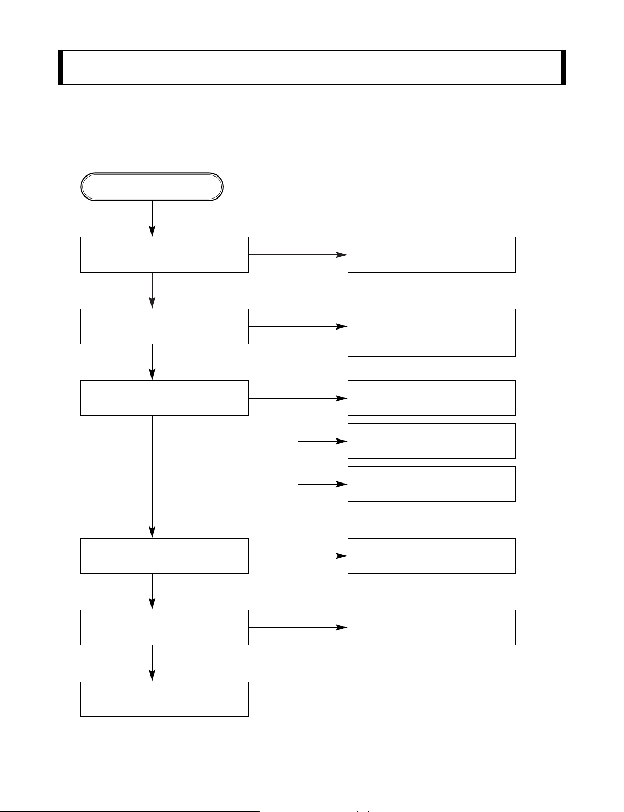
❏ ELECTRICAL TROUBLESHOOTING GUIDE
(1) No Power
ANY KEY POWER ON
YES
YES
YES
YES
YES
YES
NO
Check power supply circuitry.
Q505, Q506, IC201 Pin 39, Pin 87.
NO
Check Loading supply circuitry.
Q401~ Q404, CW001 pin25,
IC201 pin44.
NO
Check laser circuitry.
CDP P43: TR1, IC101, IC201, IC301
Check focusing circuitry.
CDP PCB: IC101, IC201, IC301.
Check DISC.
NO
Check tracking servo circuitry.
CDP PCB : IC101, IC201, IC301.
NO
Check audio circuitry.
IC201, IC302 CDP PCB: IC101, IC201.
Is power turned on?
DISC loading?
Does initial reading occur?
Can disc be played?
Is audio output supplied?
OK
- 2-2 -
(2) LCD light abnormal
ANY KEY POWER ON
(without DISC)
YES
NO
Check voltage in the power
supply circuitry.
YES
Is u-com IC201 reset circuit
normal? Pin86
4.8V
0V
NO
Power supply circuitry defective.
Q501, Q502, Q506, IC201
NO
Reset circuit defective.
IC201, Q505, Q506.
YES
Is u-com IC201 Xin,Xout terminal
Pin 1,100 input?
OSC : 4.5MHz
NO
CT201, CC201, CC202 defective.
YES
Is u-com IC201 keyin Pin7 Pin45
0volt input?
NO
CN201,front PCB pattern
defective.
YES
Is u-com IC201 Pin46, 47, 48
output waveform normal?
5V
NO
IC201 pin46~48,front PCB
pattern defective.
Is IC701 com1, com2, com3
output waveform normal?
Display LCD connector defective.
5V
NO
IC701 Surrounding circuit PCB
pattern defective.
Do display LCD then light?
- 2-3 -
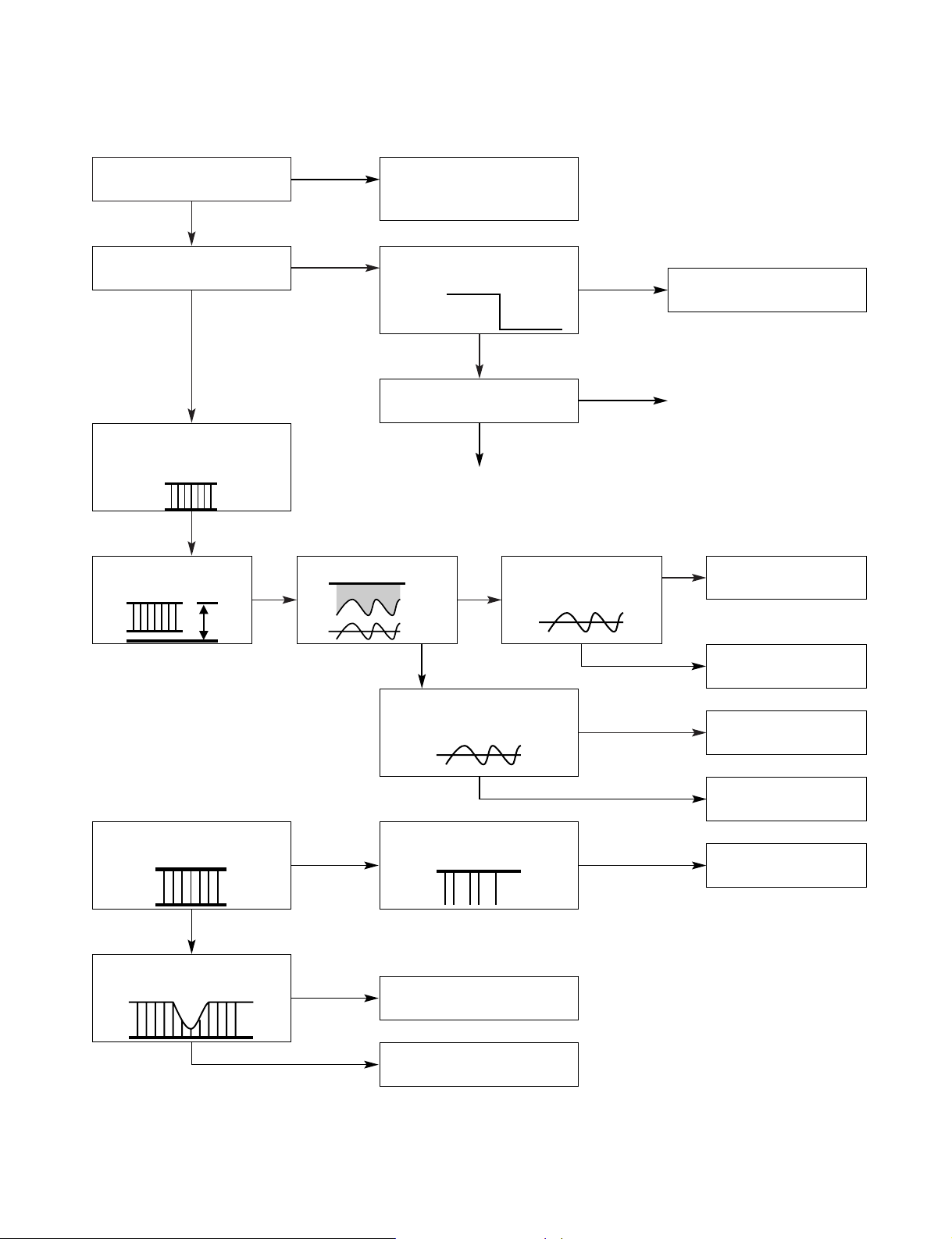
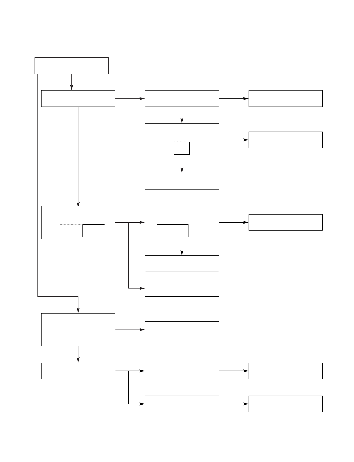
(3) Initial reading is not carried out (with disc)
DISC loading?
YES
NO
NO
NO
NO
NO
NO
NO
NO
Is IC201 pin21 input waveform
normal?
IC201
pin21
open close
YES
Does laser light?
CDP PCB: CON1 pin14(LD)
YES
YES
YES YES
Is signal output at tracking
output IC501 Pin 53 (CDP PCB)?
Does IC201 Pin25(LKFS) GFS
as figure?
Disc initial reading damaged or
defective.
Disc defective.
Is rotation normal?
Is there any irregularity in
frequency?
YES
Is RF signal normal without
dropout?
NO
Check voltage in the power
supply circuitry .
Q505, R506, IC201 pin39, pin87
CDP PCB: IC301.
NO
Leaf SW contact defective.
Connector defective.
Pattern short.
NO
(A)
(B)
Does disc motor rotate?
Is RF wave output?
RF
Is tracking servo operating?
Is the lower envelope of RF
waveform flat?
Is signal output at TEO?
Is signal output at IC101
Pin50 (CDP PCB)?
IC501
(CDP PCB)
defective.
Pattern defective.
Connector defective.
Pick-up defective.
IC502
(CDP PCB)
defective.
NO
IC201(CDP PCB) defective.
- 2-4 -
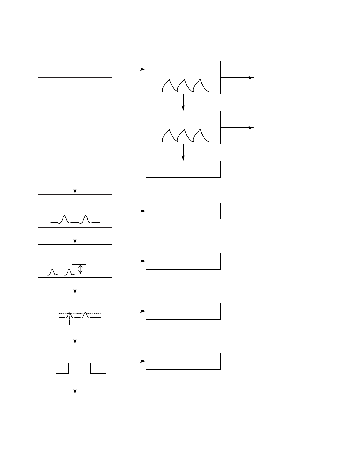
(A) when laser does not light.
Is below signal “L” at IC101
Pin 70
(CDP PCB)
?
NO
NO
NO
NO NO
NO
NO
NO
YES
Slide motor defective.
Connector defective.
YES
IC301 defective.
IC101defective.
IC101
(CDP PCB)
defective.
Surrounding circuitry defective
TR
(CDP PCB)
defective.
Connector defective.
Laser defective
Connector defective.
Laser defective
IC101,201
(CDP PCB)
defective.
NO
NO
Reset SW defective
Connector defective.
NO
IC201 defective.
Has Pick-up returned to the
innermost position?
Does pick-up stop after having
moved to the innermost position?
IC201 Pin 25
Has laser power source returned
to the TR1
(CDP PCB)
?
(TR1 collector voltage about
2.2V)
Flow laser current?
Both voltage of TR1
(CDP PCB)
is about
1.0V?
NO
YES
R40
(CDP PCB)
R40
(CDP PCB)
Are data transferred from
IC201 Pin 27, 28, 37?
Is below signal output at IC201
Pin 26,27
(CDP PCB)
?
Are detect output input at IC101
Pin38
(CDP PCB)
?
- 2-5 -
(B) when laser light.
Do lenses move up and down?
Insert disc and
in the case of
check of initial
leading.
Is RF(HF) signal waveform
output?
NO
NO
Is signal output at focus search
terminal? IC101 Pin48
(CDP PCB)
NO
IC101
(CDP PCB)
defective.
Is signal output at IC301
Pin1, 2
(CDP PCB)
?
NO
IC301 defective.
YES
YES
YES
Actuator short.
Connector short.
IC101
(CDP PCB)
defective.
Connector short.
The waveform of RF(HF) is
below figure?
Amplitude
0.5~1.0v
NO
YES
IC101
(CDP PCB)
defective.
TR1, IC101
(CDP PCB)
surrounding circuitry
defective.
Is FOK signal output? RF(HF)
0.4V over OK.
FOK
NO
YES
IC101
(CDP PCB)
defective.
Is FOK signal to IC201 Pin41?
(C)
FOK
NO
YES
Pattern defective.
YES
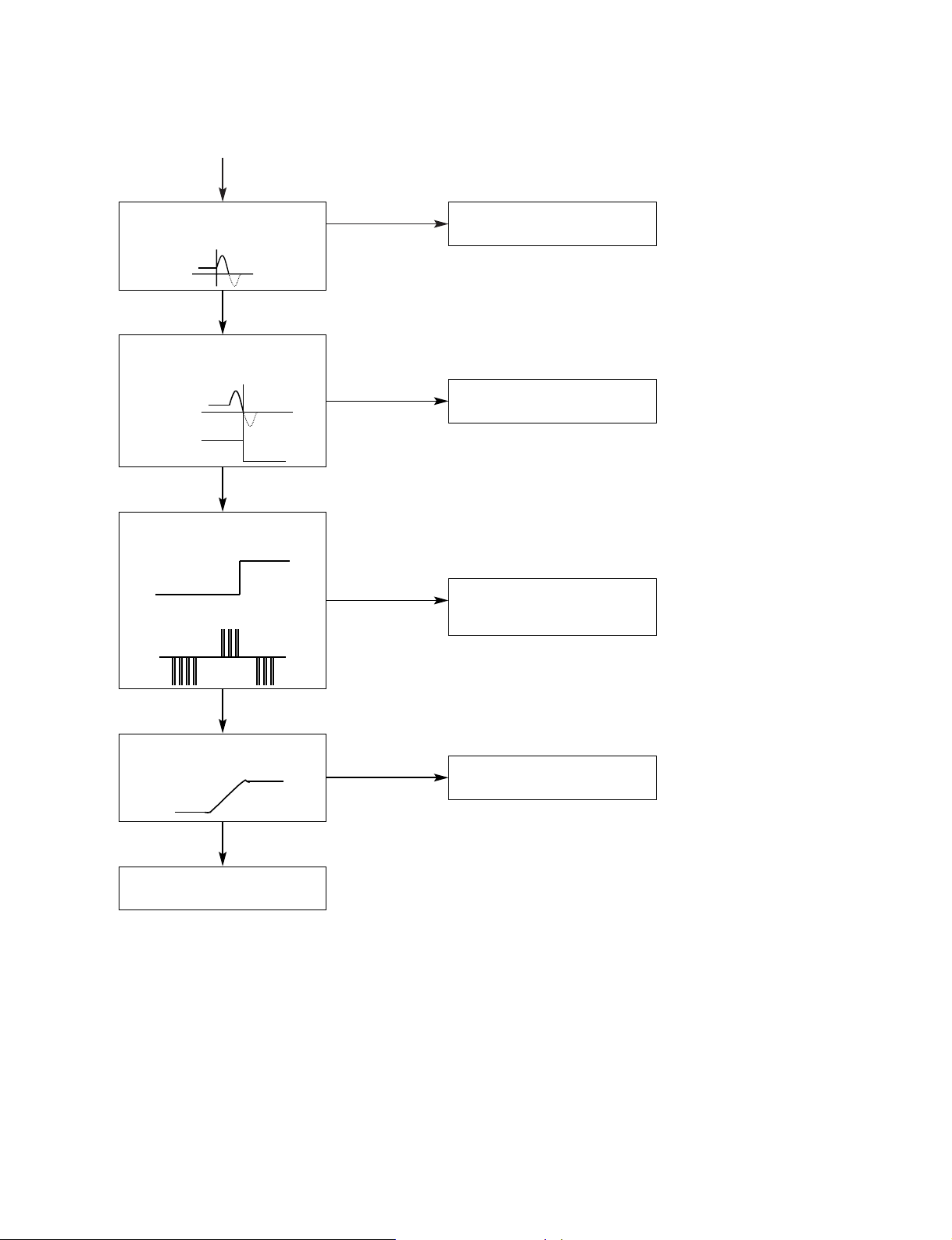
- 2-6 -
(C)
YES
NO
IC101
(CDP PCB)
defective.
Pick-up defective.
Connector defective.
Is FE1 signal output ?
IC501 Pin59
YES
NO
IC101
(CDP PCB)
defective.
Is FE1 signal output at IC101
(CDP PCB)
Pin31(IST
AT) ?
YES
NO
Pattern defective between IC201
Pin 72, 73, 75, 76 (CDP PCB)
and IC201(Main).
Is SMON signal output by IC201
(CDP PCB)
Pin73?
Is SMPO signal output by IC201
(CDP PCB)
Pin75?
YES
NO
IC101,305
(CDP PCB)
defective.
Surrounding circuitry defective.
Has voltage at disc motor?
0v
YES
Disc motor defective.
CN101(CDP PCB) connector defective.
IS TAT
FE1
- 2-7 -
❏
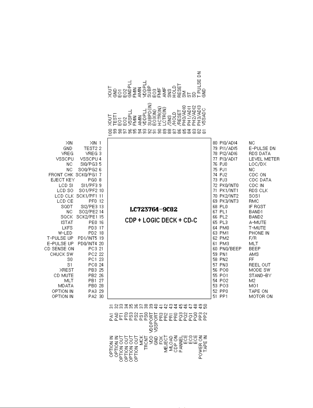
INTERNAL BLOCK DIAGRAM of ICs
■ IC201 LC723764 (Micro-processor IC)
1) PORT ASSIGNMENT
 Loading...