

Page 1

- 1-1 -
❍
SECTION 1. SUMMARY
• SERVICING PRECAUTIONS
..........................................................................................................
1-2
• ESD PRECAUTIONS
.......................................................................................................................
1-3
• SPECIFICATIONS
...........................................................................................................................
1-4
❍
SECTION 2. ELECTRICAL
• ADJUSTMENTS
..............................................................................................................................
2-1
• ELECTRICAL TROUBLESHOOTING GUIDE
.................................................................................
2-1
• WAVEFORMS OF MAJOR CHECK POINT
....................................................................................
2-1
• INTERNAL BLOCK DIAGRAM of ICs
..............................................................................................
2-7
• BLOCK DIAGRAM
.........................................................................................................................
2-29
• SCHEMATIC DIAGRAM
................................................................................................................
2-31
• MAIN SCHEMATIC DIAGRAM
......................................................................................................
2-33
• CDP SCHEMATIC DIAGRAM
.......................................................................................................
2-35
• PRINTED CIRCUIT DIAGRAM
......................................................................................................
2-37
❍
SECTION 3. CABINET MAIN CHASSIS & MECHANISM
• EXPLODED VIEW
...........................................................................................................................
3-1
❍
SECTION 4. REPLACEMENT PARTS LIST
...................................................................
4-1
[CONTENTS]
Page 2

- 1-2 -
❏ SERVICING PRECAUTIONS
➊ Always disconnect the power source before:
1) Removing or reinstalling any component, circuit board, module or any other instrument assembly.
2) Disconnecting or reconnecting any instrument electrical plug or other electrical connection.
3) Connecting a test substitute in parallel with an electrolytic capacitor in the instrument.
CAUTION: A wrong part substitution or incorrect polarity installation of electrolytic capacitors may result in
an explosion hazard.
➋ Do not defeat any plug/socket B+ voltage interlocks with which instruments covered by this service
manual might be equipped.
❸ Do not apply power to this instrument and or any of its electrical assemblies unless all solid-state
device heat sinks are correctly installed.
❹ Always connect a test instrument’s ground lead to the instrument chassis ground before
connecting the test instrument positive lead. Always remove the test instrument ground lead last.
1) The service precautions are indicated or printed on the cabinet, chassis or components. When servicing,
follow the printed or indicated service precautions and service materials.
2) The Components used in the unit have a specified conflammability and dielectric strength. When
replacing any components, use components which have the same ratings. Components marked in
the circuit diagram are important for safety or for the characteristics of the unit. Always replace with the
exact components.
3) An insulation tube or tape is sometimes used and some components are raised above the printed writing
board for safety. The internal wiring is sometimes clamped to prevent contact with heating components.
Install them as they were.
4) After servicing always check that the removed screws, components and wiring have been installed
correctly and that the portion around the service part has not been damaged. Further check the insulation
between the blades of attachment plug and accessible conductive parts.
SECTION 1. SUMMARY
Page 3
- 1-3 -
❏
ESD PRECAUTIONS
[Electrostatically Sensitive Devices (ESD)]
Some semiconductor (solid state) devices can be damaged easily by static electricity. Such omponents
commonly are called Electrostatically Sensitive Devices (ESD). Examples of typical ESD devices are
integrated circuits and some field-effect transistors and semiconductor chip components. The following
techniques should be used to help reduce the incidence of component damage caused by static electricity.
1) Immediately before handling any semiconductor component or semiconductor-equipped assembly, drain
off any electrostatic charge on your body by touching a known earth ground. Alternatively, obtain and
wear a commercially available discharging wrist strap device, which should be removed for potential
shock reasons prior to applying power to the unit under test.
2) After removing an electrical assembly equipped with ESD devices, place the assembly on a conductive
surface such as aluminum foil, to prevent electrostatic charge buildup or exposure of the assembly.
3) Use only a grounded-tip soldering iron to solder or unsolder ESD devices.
4) Use only an anti-static solder removal device. Some solder removal devices not classified as “anti-static”
can generate electrical charges sufficient to damage ESD devices.
5) Do not use freon-propelled chemicals. These can generate electrical charges sufficient to damage ESD
devices.
6) Do not remove a replacement ESD device from its protective package until immediately before you are
ready to install it. (Most replacement ESD devices are packaged with leads electrically shorted together
by conductive foam, aluminum foil or comparable conductive material).
7) Immediately before removing the protective material from the leads of a replacement ESD device, touch
the protective material to the chassis or circuit assembly into which the device will be installed.
CAUTION: Be sure no power is applied to the chassis or circuit, and observe all other safety precautions.
8) Minimize bodily motions when handling unpackaged replacement ESD devices. (Otherwise harmless
motion such as the brushing together of your clothes fabric or the lifting of your foot from a carpeted floor
can generate static electricity sufficient to damage an ESD device).
[CAUTION. GRAPHIC SYMBOLS]
THE LIGHTNING FLASH WITH APROWHEAD SYMBOL. WITHIN AN EQUILATERAL
TRIANGLE, IS INTENDED TO ALERT THE SERVICE PERSONNEL TO THE PRESENCE
OF UNINSULATED “DANGEROUS VOLTAGE” THAT MAY BE OF SUFFICIENT
MAGNITUDE TO CONSTITUTE A RISK OF ELECTRIC SHOCK.
THE EXCLAMATION POINT WITHIN AN EQUILATERAL TRIANGLE IS INTENDED TO
ALERT THE SERVICE PERSONNEL TO THE PRESENCE OF IMPORTANT SAFETY
INFORMATION IN SERVICE LITERATURE.
Page 4
- 2-1 -
❏ ADJUSTMENTS
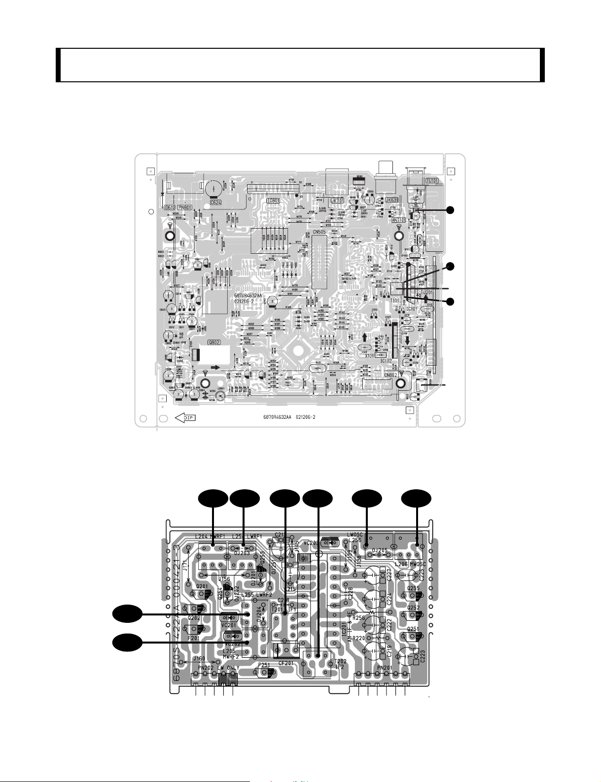
1. Test & Adjustment point
Figure 1. MAIN PCB Board
Figure 2. BEFORE RF PCB Board
L204
L255
L205
L254 T201 T202 T256 T206
T101
RV101
A
B
C
SECTION 2. ELECTRICAL
Page 5
- 2-2 -
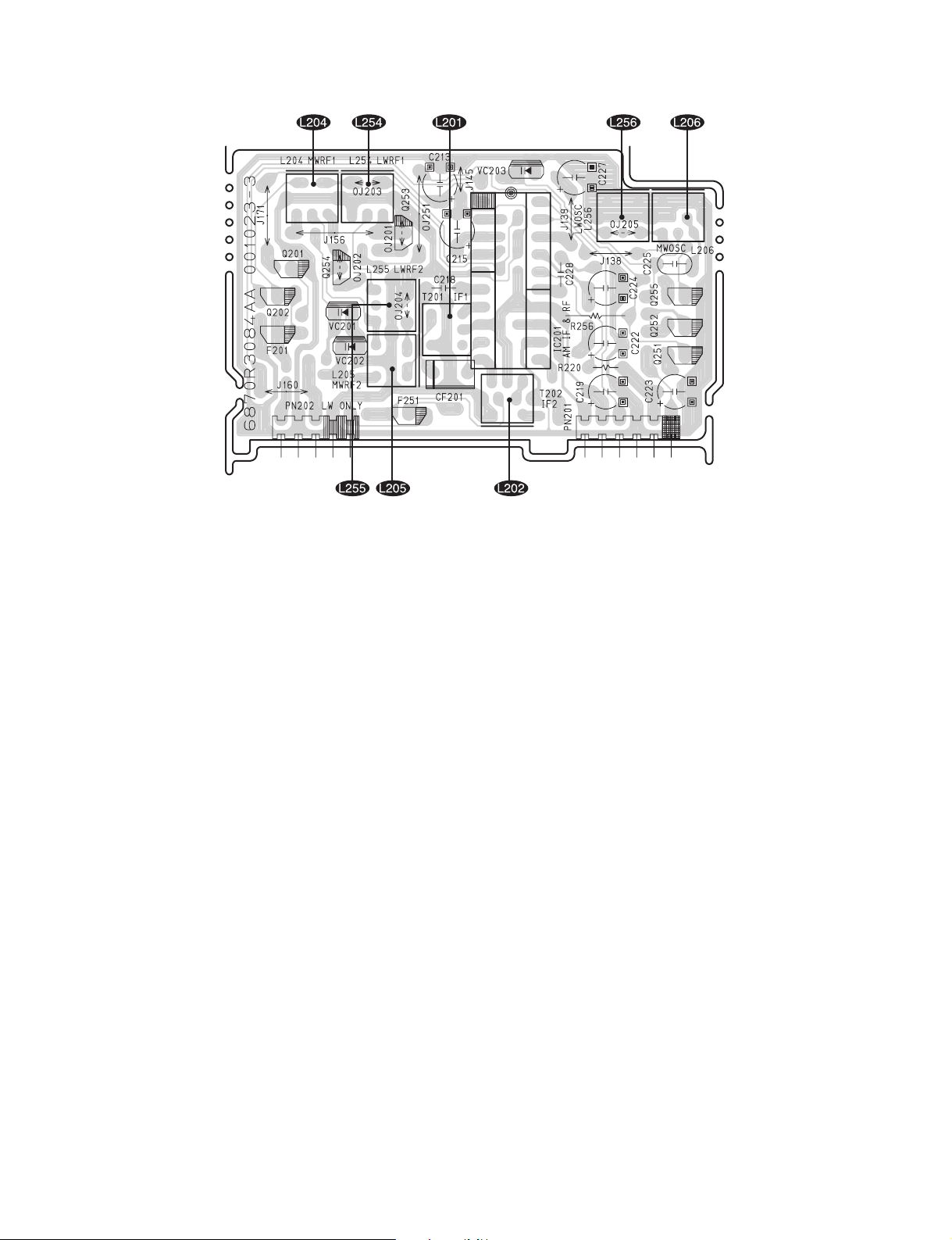
( NEW RF P.C. BOARD)
Figure 3. NEW RF PCB Board
Page 6
- 2-3 -
2. FM Adjustment
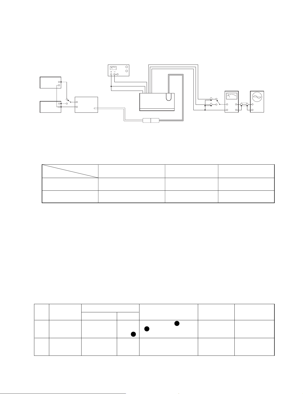
Figure 4.
(1) The impedance of FM antenna terminal is 75Ω.
Therefore, connect coaxial cable (3C-2V etc.) between FM SG and antenna terminal when wiring.
(2) There are two kind in indication of FM SG output attenuator.
1) Attenuator with Marking of 75Ω open...open indication type
2) Attenuator with marking of 75Ω load or close...load or close indication type.
(3) FM SG output level in this FM adjustment are described as open indication type. The up table shows
relations among FM SG attenuator indication(dB), available power ratio(dBf) and antenna terminal
voltage(dB/µV) in each indication type.
Notes:
1. BAND Switch ········································································································································ FM
2. BALANCE ······································································································································· Center
3. TREBLE/BASS ································································································································ Center
4. Connect as shown in figure 3.
5. Refer to figure 1~2 for Adjustment Points.
Item FM SSG Attenuator Available Antenna
Type Indication Power Ratio Terminal Voltage
Open indication type 0dB 5.2dBf 6dB/µV
60dB 65.2dBf 66dB/µV
Load or close 0dB 11.2dBf 12dB/µV
indication type 54dB 65.2dBf 66dB/µV
FEED SIGNAL
STEP SUBJECT
FROM TO
MEASURE OUTPUT ADJUSTMENT ADJUST FOR
1 Discriminator 98MHz 60dB ANT Jack Between Point XX & Point T101 DC 0V±10mV
22.5kHz Dev. or XX, DC Volt Meter.
1kHz FM SSG Point XX
2 MPX 98MHz 60dB Same as Channel speration RV101 30dB
Adjustment
75kHz Dev.1kHz
above
FM SSG
A
B
C
Stereo modulator
AUDIO OSC
SSG
GND
(Black Lead)
PRE OUT
(Red Lead)
(Yellow Lead)
Power Supply
OUT
EXT
MODE
ANT
Jack.
VTVM SCOPE
IN OUT
Unit
Page 7
- 2-4 -
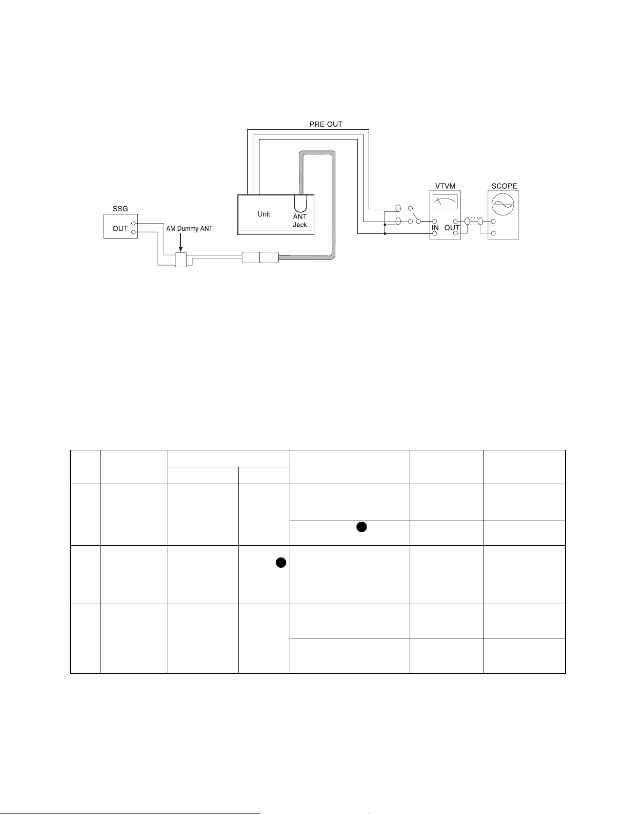
3. AM(MW) Adjustment
Notes:
1. BAND Switch ··································································································································· AM(MW)
2. Connect as shown in figure 4.
3. Refer to figure 1~2 for Adjustment Points.
Figure 5.
FEED SIGNAL
STEP SUBJECT
FROM TO
MEASURE OUTPUT ADJUSTMENT ADJUST FOR
1 520 or 522kHz No Input LCD Display TUNE +/- Button 520 or 522kHz
(Reception Frequency)
Tuning Voltage Between Point XX and GND, L206 DC 1.2V±0.05V
Adjustment DC Volt Meter
2 IF Coil 600kHz or ANT Jack Output L or R ch, T201 & T202 Max. Output
Adjustment 603kHz ANT or PointXX VTVM & Oscilloscope
input, 30dB,
400Hz (30%
MOD) SSG.
3 600kHz or 600kHz or Same as LCD Display TUNE +/- Button 600 or 603kHz
603kHz 603kHz ANT above (Reception Frequency)
RF Adjustment input, 30dB,
400Hz (30%
Output L or R ch, L204 & L205 Max. Output
MOD) SG.
VTVM & Oscilloscope
A
B
Page 8
- 2-5 -
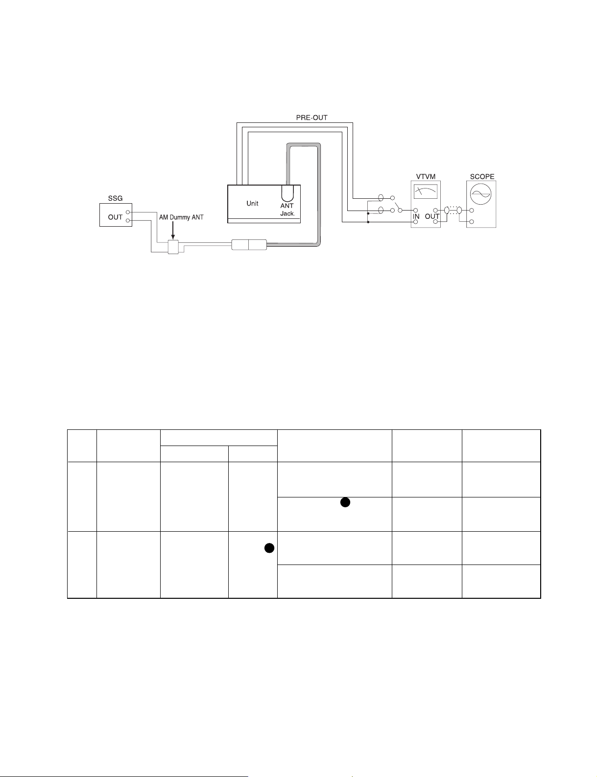
4. LW Adjustment(Optional)
Notes:
1. BAND Switch ··········································································································································· LW
2. Connect as shown in figure 5.
3. Refer to figure 1~2 for Adjustment Points.
Figure 6.
FEED SIGNAL
STEP SUBJECT
FROM TO
MEASURE OUTPUT ADJUSTMENT ADJUST FOR
1 144kHz No Input LCD Display TUNE +/- Button 144kHz
(Reception Frequency)
Tuning Voltage Between Point XX and GND, L256 DC 1.2V±0.05V
Adjustment DC Volt Meter
2 150kHz 150kHz ANT Jack LCD Display TUNE +/- Button 150kHz
RF Adjustment ANT input, or PointXX (Reception Frequency)
30dB, 400Hz
(30% MOD)
Output L or R ch, L254 & L255 Max. Output
SSG.
VTVM & Oscilloscope
A
B
Page 9
- 2-6 -
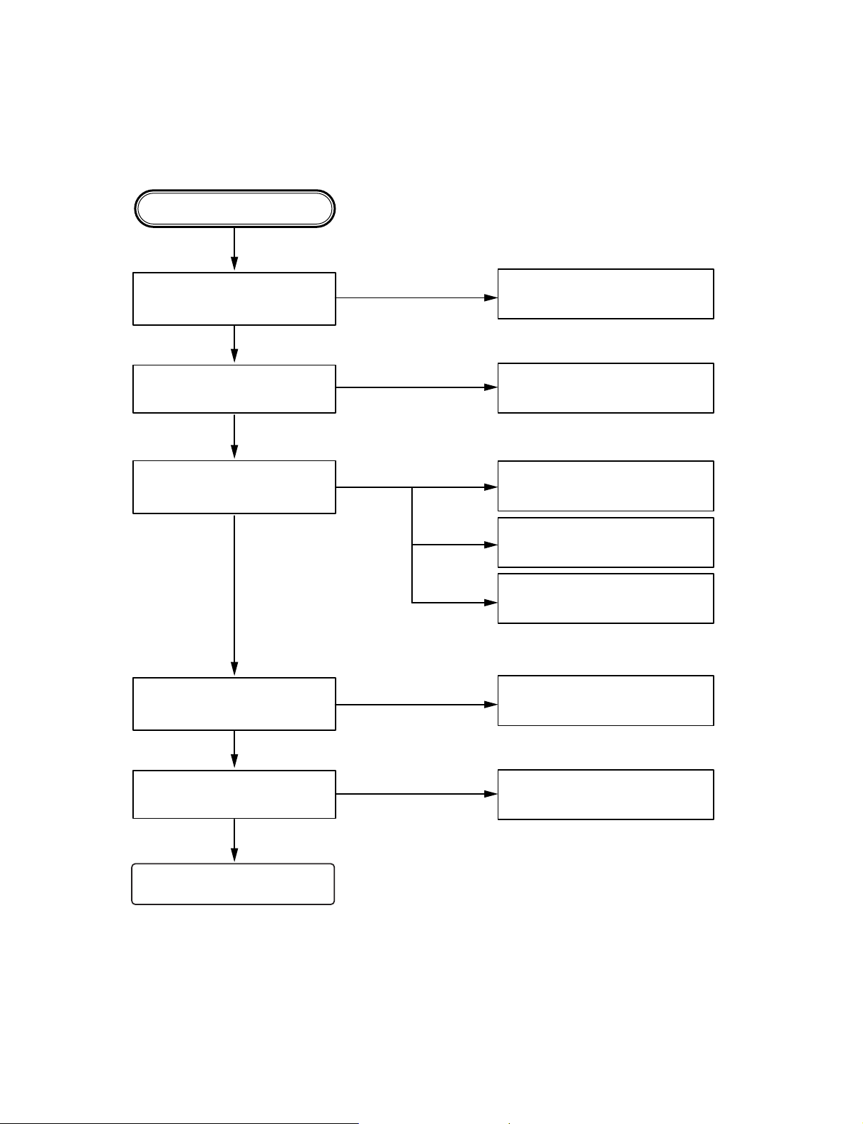
❏ ELECTRICAL TROUBLESHOOTING GUIDE
Any Key power on.
Is power turnd on?
DISC loading?
Does initial reading occur?
Can disc be played?
Is audio output supplied?
Check power supply circuitry.
Q808, Q809, Q802, IC401,
PIN13
Check loading supply circuitry.
Q505, Q506, Q507, IC401, CN505
Check laser circuitry.
Q501, IC501, IC503, IC504
Check focusing circuitry.
IC501, IC503
Check DISC.
Check tracking servo circuitry.
IC501, IC503
Check audio circuitry.
IC501, IC401, IC601, IC801
OK
YES
YES
YES
YES
YES
YES
NO
NO
NO
NO
NO
(1) No Power.
Page 10
- 2-7 -
YES
YES
YES
YES
YES
YES
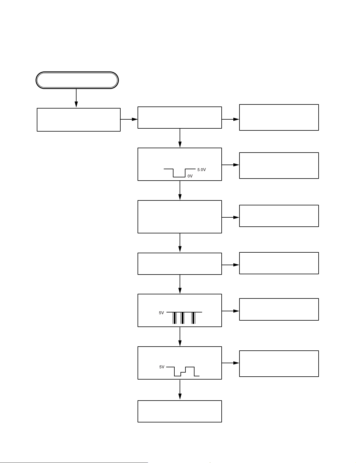
(2) LCD light abnornal.
Any Key power on.
(without DISC)
Do display LCD then light?
Check voltage in the power
supply circuitry.
Power supply circuitry
defective.
Q802, Q807, Q808, Q809
Reset circuit defective.
Q803,Q804 Surrounding
circuit defective.
X401, C410, C411 defective.
Q807, CN802 front PCB
pattern defective.
IC401, Pin45~48 front PCB
pattern defective.
IC901, Surrounding circuit
PCB pattern defective.
Is u-com IC401 reset circuit
normal? Pin53
Is u-com IC401 keyin Pin17, 18
5volt input?
Is u-com IC401 Pin45, Pin48
output waveform normal?
Is IC901 Com1, Com2, Com3
output waveform normal?
Display LCD connector defective.
Is u-com IC401X1, X2 terminal
pin 57.58 input?
OSC : 7.2MHz
NO
NO
NO
NO
NO
NO
NO
Page 11
- 2-8 -
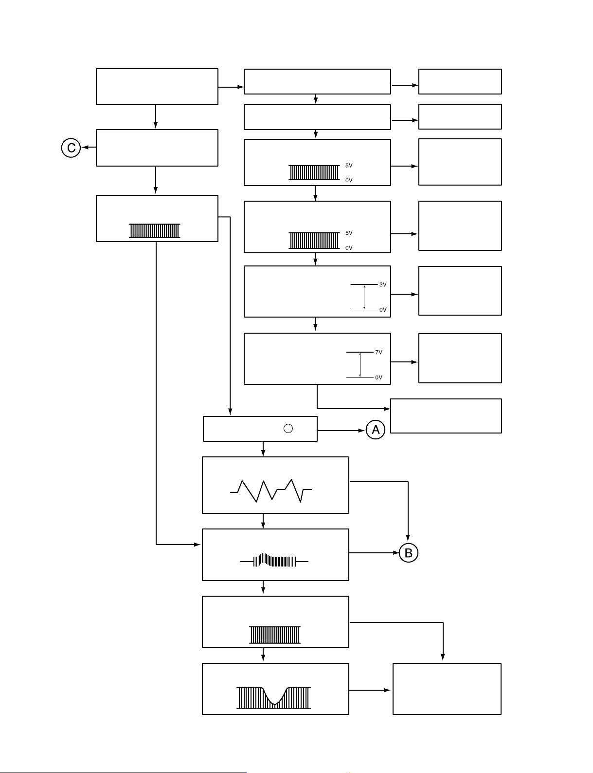
(3) Initial reading is not carried out.
NO
NO
NO
NO
NO
NO
NO
NO
NO
NO
NO
NO
YES
YES
YES
YES
YES
YES
YES
YES
YES
YES
YES (with disc)
YES
YES
Slide motor moves
(Without disc)
Spindle motor turns
Does RF waveform appear?
IC501 Pin7
Check the Data transmission from
PN505 PIN7,8,20 to CD DSP
Check the Data transmission from
PN505 PIN19 to MICOM
Check the change of
SLPWMF Voltage
(IC503 PIN23)
Check the change of SL +,
SL - Voltage
(IC503 pin 13, 14)
Check the Voltage change of PN 505
PIN15 (7.5V)
Check the Voltage IC 501 PIN12
(1.4V~1.8V)
Defective connector
PN505
Defective IC 501
Defective connector
PN505
Defective MICOM
Defective connector
PN505
Defective IC501
Defective IC501
Defective IC503
Defective contact PN502
Defective PICK-UP
Laser light check A ?
focus coil drive wareform.
TRACKING ERROR wareform
Is rotation normal?
Defective IC501
Defective PICK-UP
Is there no dropout of RF signal?
Does FA+ waveform appear at
IC503 pin15?
Does TE waveform appear at
IC501 pin 11?
Page 12
- 2-9 -
NO
NO
NO
NO
NO
NO
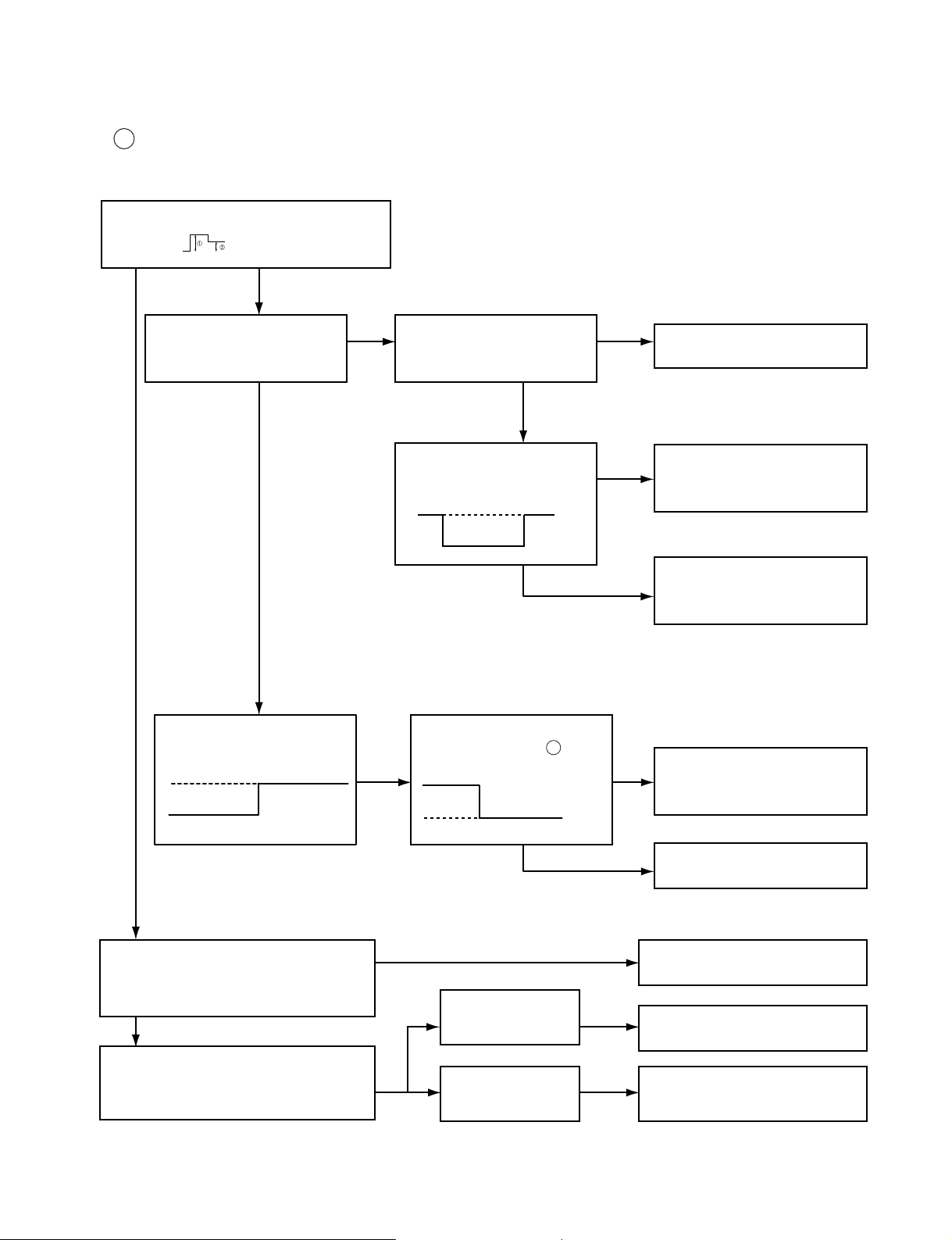
When laser does not light.
Is “2.4V~3.4V” applied to pin 19 of IC 501?
( ➀ 3.4V ➁ 2.4V)
Is power supplied to laser Q501?
(Q 501 collector: about 1.8V)
Does laser current flow?
1.0V across R555
Is data transferred from
MICOM IC ?
Does voltage appear at IC
503 pin 13, 14?
Defective MICOM.
Defective MICOM.
Defective connector. (PN 501)
Defective IC 501, 503
Defective slide motor and/or
connector.
Defective LMT SW and/or
connector. (PN 502)
Defective Q 501 and/or laser.
Defective laser and/or
connector. (PN 501)
Did pickup return to
innermost circular?
Does it stop at inner pick
circular after shift?
Is defect output from LMT
SW applied to pin of
PN505?
R555 »1.0V
R555 «1.0V
YES
YES
YES
YES
OPEN
CLOSE
YES
YES
YES
YES
YES
YES
A
2
OV
Page 13
- 2-10 -
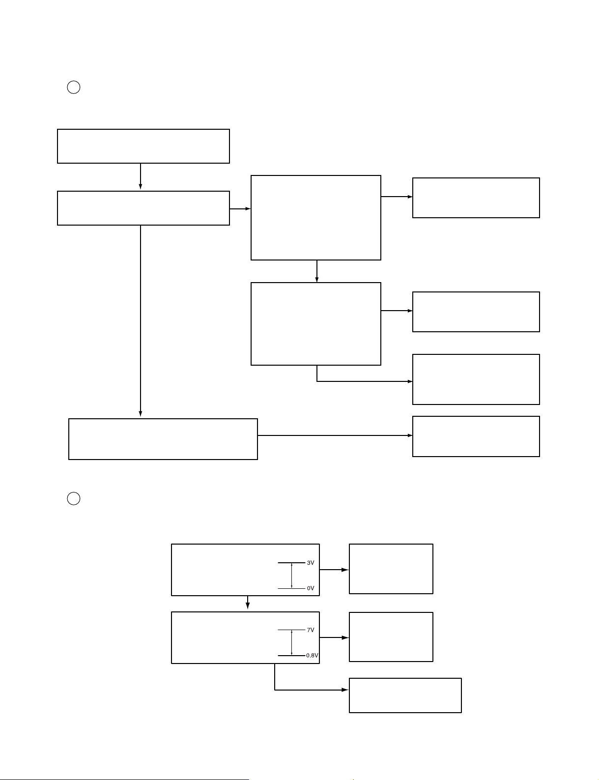
When laser light.
B
When SPINDLE motor dose not turn
C
NO
NO
NO
NO
YES
YES
YES
YES
Laser lights
Check the signal of
FOCUS SEARCH
(IC503 Pin 26)
Chekc the signal of IC503
pin 15, 16
Does FE signal appear?
(IC501 pin 9)
Does DRF signal appear? (IC 501 pin67)
Defective IC501
Defective IC503
Open activator and/or
connector
(PN501)
Degraded laser diode
Defective PICK-UP
YES
NO
NO
YES
Check the change of
SPPWMF Voltage
(IC503 pin26)
Check the change of SP +,
SP -, Voltage
(IC503 pin 11, 12)
Defective IC501
Defective IC503
Defective contact PN502
Defective PICK-UP
Page 14
- 2-11 -
(CH1)
(CH2)
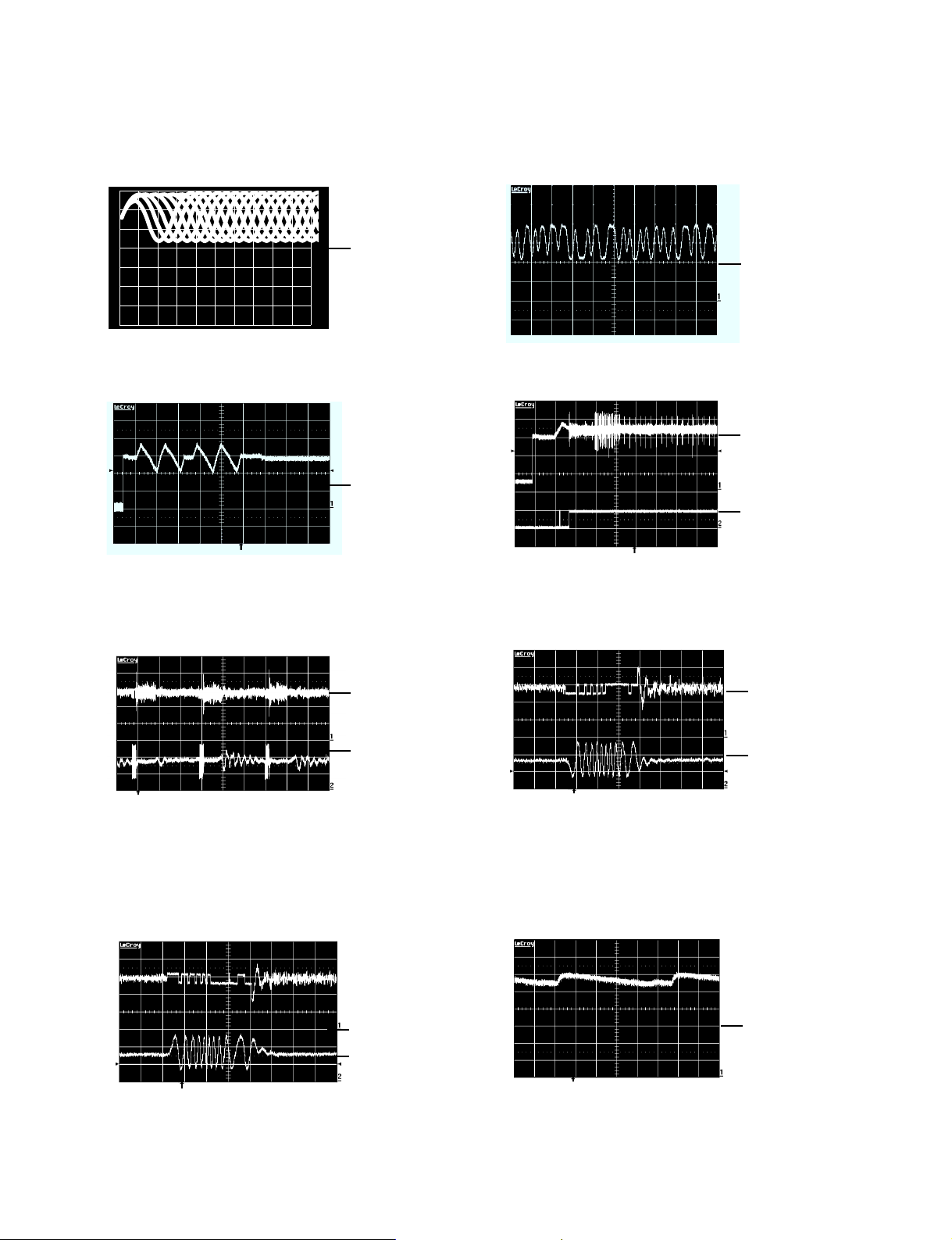
❏ WAVEFORMS OF MAJOR CHECK POINT
1. HF signal (RF signal ) waveform
(IC501 pin 7) during normal play
2. EFM signal (IC501 pin 6)waveform
during Normal Play
3. Focus coil drive waveform(IC503 pin15)
• When focus search failed or there is no disc on the tray
• Focus coil drive waveform(IC503 pin26) and DRF(IC501
pin67) when focus search is accomplished
4. Tracking coil drive waveform and TE during track
traverse
(1) When time division is 20mS/Div.1V/Div.
(2) When time division 1mS/Div, 1V/Div
(During forward track traverse)
(3) When time division is 0.5nS/div.
(During backward Track Traverse)
5. Feed motor drive waveform(IC 503 pin14)
During normal play
CH1 : FOCUS COIL DRIVE
SIGNAL 2V/Div.
CH2 : DRF
CH1 : TRACKING COIL DRIVE
SIGNAL 2V/Div. (IC503 pin17)
CH2 : TRACKING ERROR(TE: IC501 pin11)
1V/Div.
(
(
(
CH1 : TRACKING COIL DRIVE (IC503 pin17)
SIGNAL 2V/Div.
CH2 : TRACKING ERROR (TE: IC501 pin11)
1V/Div.
(
CH1 : TRACKING COIL DRIVE (IC503 pin17)
CH2 : TRACKING ERROR (TE: IC501 pin11)
(
0.5V/Div.
500nS/Div.
(
1S/Div.
1V/Div.
(
1mS/Div.
1V/Div.
(
0.5V/Div.
5µS/Div.
(
2S/Div.
0.5V/Div.
OV
OV
OV
(CH1)
(CH2)
(CH1)
(CH2)
(CH2)
OV
OV
OV
OV
OV
OV
OV
OV
OV
Page 15
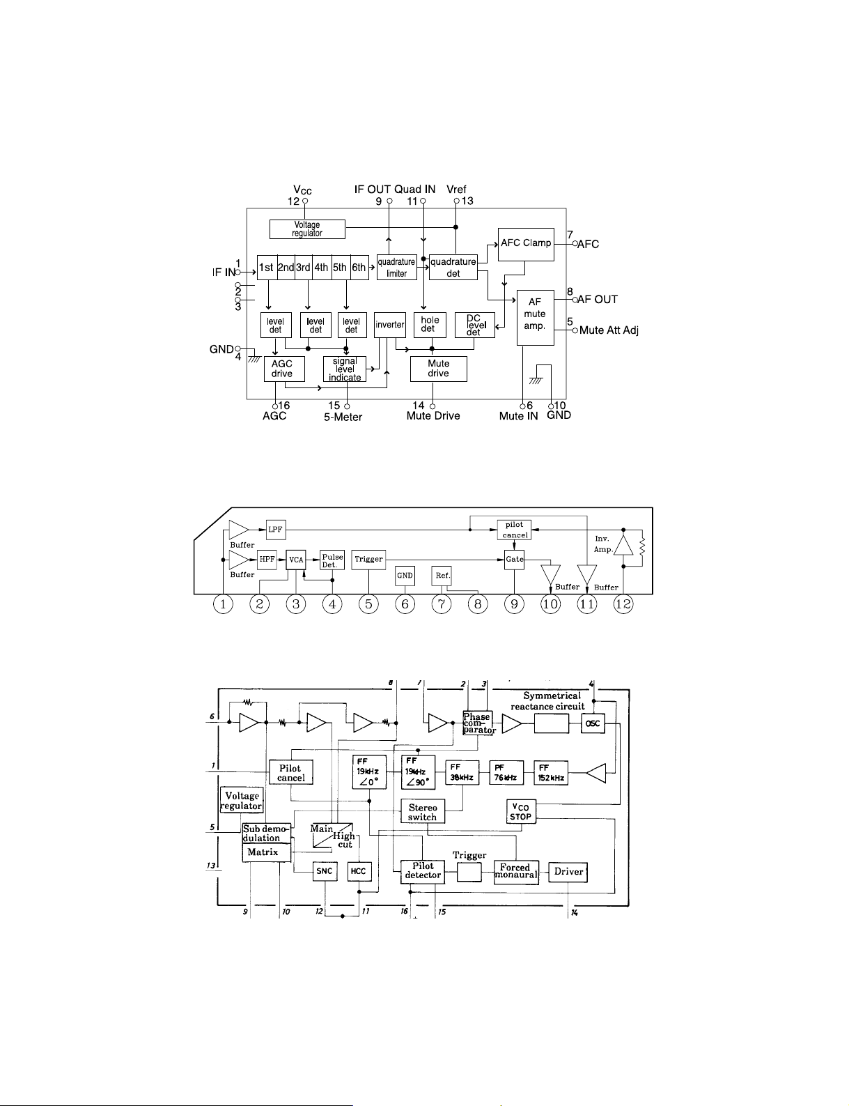
- 2-12 -
❏
INTERNAL BLOCK DIAGRAM of ICs
■ IC101 LA1140
■ IC102 KIA6010SN
■ IC103 LA3430M
Page 16
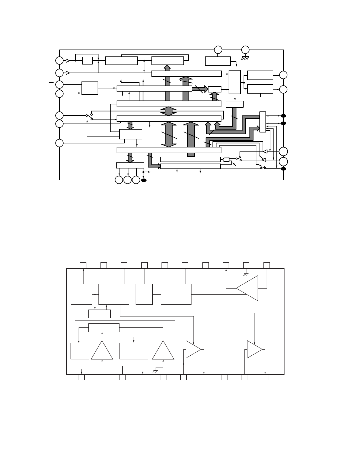
- 2-13 -
NOTE: Mark terminals are not existence in KIC9256P, KIC9256F
Terminal name of KIC9256P, KIC9256F is shown in parentheses.
Others are common terminals.
■ IC104 KIC9256P
POWER ON
RESET
TRI-STATE
BUFFER
TRI-STATE
BUFFER
RESET
PHASE
COMPARATOR
OSC
CIRCUIT
24bit REGISTER
ADDRESS
DECODER
20bit BINARY COUNTER
UNIVERSAL COUNTER CONTROL
OUTPUT PORT
24bit REGISTER
4
FM
1mS
OSC
MODE LF
4
UNLOCK
1/0 PORT
8
TEST
24 22
5
5
10
12 bit PROGRAMMABLE COUNTER
MAX
12
15
4
OT4
DO1
DO2
(DO2/OT-4)
1/0-5/CLK
1/0-6
1/0-9 IF
IN2
(1/0-6 IF )
IN2
1/0-8 IF
IN1
1/0-7 SC
IN
(1/0-5 IF )
IN1
4
15
129
16
13
14
8
OT-4
OT-2
OT-3
OT-4
OT-1
XT 1mS
GATE
AMP
AMP
7
6
3
4
5
1
2
10
11
1/2
FM
FM
PSC
V
DD
GND
AMP
HF
FM
IN
AM
IN
XT
XT
DATA
CLOCK
PERIOD
S
L
2 MODULUS
PRESCALER
4 bit SWALLOW
COUNTER
REFERENCE COUNTER
24bit SHIFT REGISTER
■ IC201 DBL 1019
LOCAL
OSC
BUFFER
LOCAL
OSC
RF
AGC
ATTENUATOR
DRIVER
MIX
IF
AMP
IF
DETECTOR
RF
AMP2
RF
AMP2
IF
AGC
SIGNAL
METER
ALC
RF DETECTOR
20 19 18 17 16 15 14 13 12 11
12345678910
Local OSC
Butter Out
RFAGC
Out
RFAmp2InRF
AGC
GND MIX in &
RF AMP1 In
MIX
Out
IF AmpInIF Amp
Out
ANT Damping
Driver
Local
OSC2
Local
OSC1
Signal
Meter Out
Signal
Meter In
Detector
Out
Detector
InGND
V
CC
V
CC
IF
AGC
Page 17
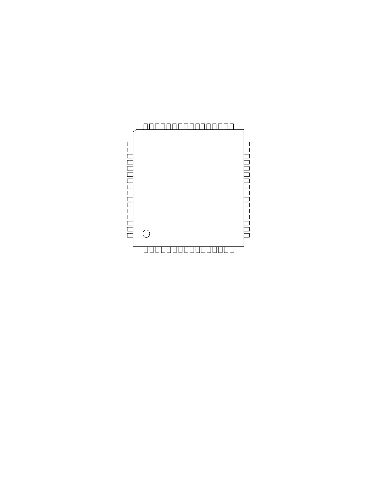
- 2-14 -
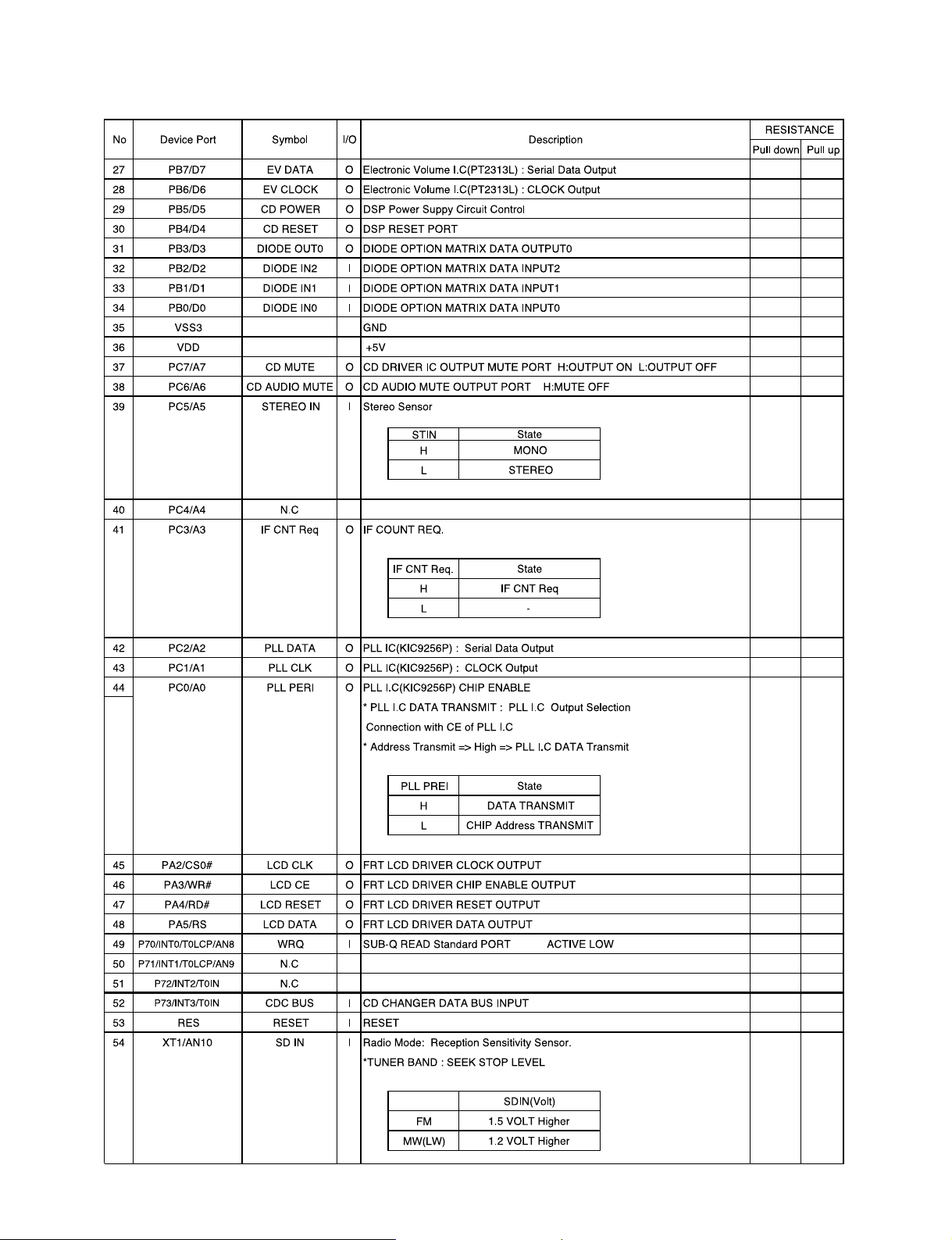
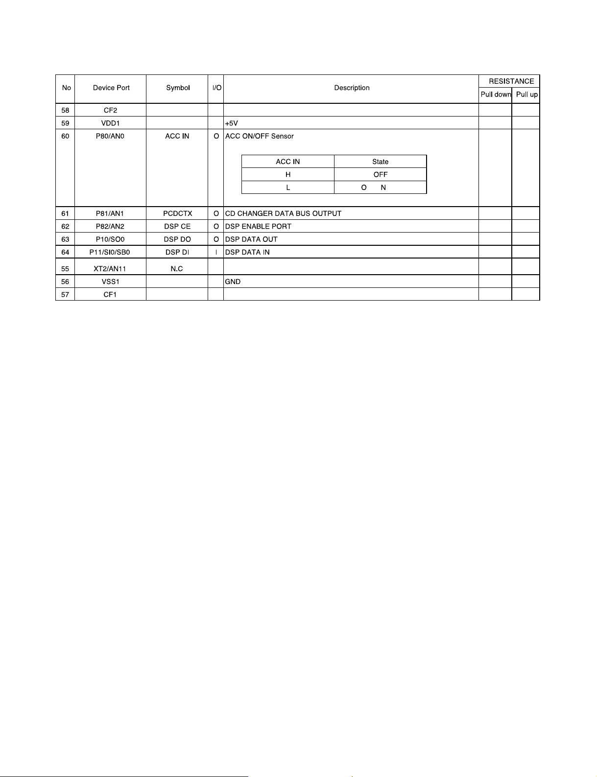
■ IC401 LCD875747B
484746454443424140
39
3837363534
33
49
50
51
52
53
54
55
56
57
58
59
60
61
62
63
64
123456789
10
1112131415
16
(I) PCD_WRQ P70/INT0/T0LCP/AN8
N.C P71/INT1/T0HCP/AN9
N.C P72/INT2/T0IN
(I) PCDCBUS
P73/INT3/T0IN
RES#
(I) PSDIN XT1/AN3
XT2
VSS1
CF1
CF2
VDD1
(I) PACCIN P80/AN0
(I) PCDCTX P81/AN1
(O) PCD_CE P82/AN2
(O) PCD_DO P10/SO0
(I) PCD_DI P11/SI0/SB0
(O) PCD_CL P12/SCK0
(O) PCDCON P13/SO1
(I) PVOLA P14/SI1/SB1
(I) PVOLB P15/SCK1
(O) PLED P16/T1PWML
(O) PBEEP P17/T1PWMH/BUZ
PWM1
PWM0
VDD2
VSS2
N.C P00
(O) PPWR_MUTE P01
(O) PPOWER P02
N.C P03/AN3
(I)PEJT_KEY P04/AN4
(I) PKEY1 P05/AN5
PB2/D2 (I) PDIOIN2
PB3/D3 (O) PDIOOUT0
PB4/D4 (O) PCD_RESET
PB5/D5 (O) PCD_POWER
PB6/D6 (O) PEVCLK
PA5/RS (O) PFSO
PA4/RD# (O) PFINH
PA3/WR# (O) PFCE
PA2/CS0# (O) PFCLK
PC0/A0 (O) PPLLCE
PC1/A1 (O) PPLLCLK
PC2/A2 (O) PPLLDATA
PC3/A3 (O) PAGC
PC4/A4 N.C
PC5/A5 (I) PSTIN
PC6/A6 (O) PCD_AMUTE
PC7/A7 (O) PCD_MUTE
VDD3
VSS3
PB0/D0 (I) PDIOIN0
PB1/D1 (I) PDIOIN1
IC401
LC875747B
P23/INT4/T1IN (O) PCD_WOK
P22/INT4/T1IN (I) PCD_CNTOK
P21/INT4/T1IN (I) PCD_OVF
P20/INT4/T1IN (I) PCD_FSEQ
P07/AN7 (I) PLEVEL
P06/AN6 (I) PKEY2
32
31
30
29
28
27
26
25
24
23
PB7/D7 (O) PEVDATA
P27/INT5/T1IN (I)PMECHA_SW1
P26/INT5/T1IN (I)PCD_DRF
P25/INT5/T1IN (I)PMECHA_SW2
P24/INT5/T1IN (I)PLIMIT_SW
22
21
20
19
18
17
Page 18
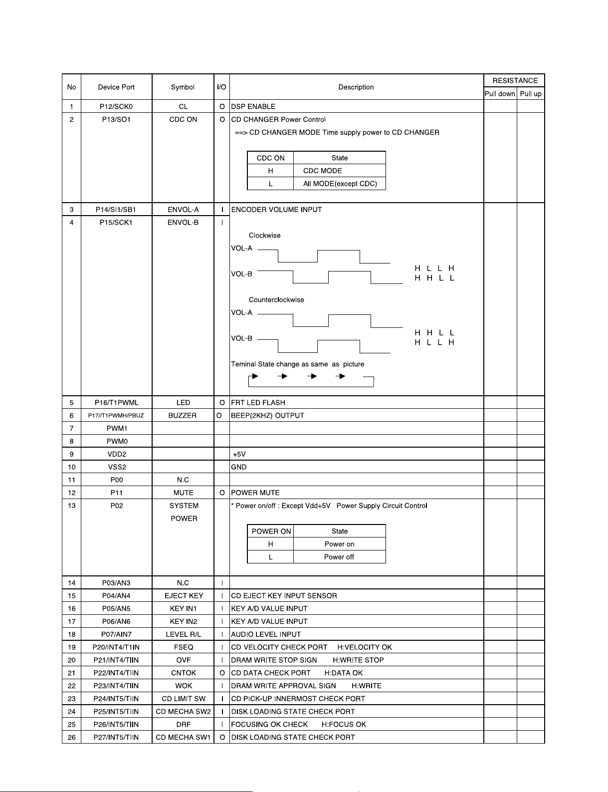
- 2-15 -
■ PIN Function
①②③
④
①②③
④
①
②
③
④
Page 19
- 2-16 -
Page 20
- 2-17 -
Page 21
- 2-18 -
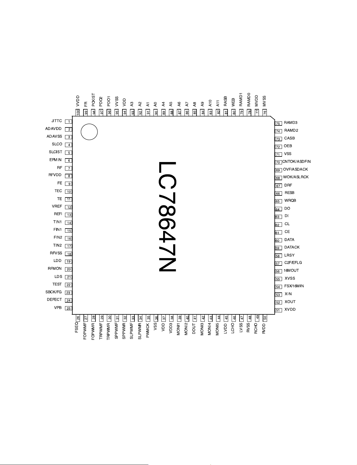
■ IC501 LC78647N
Page 22
- 2-19 -
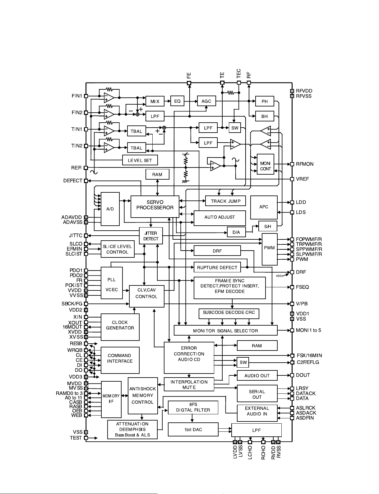
■ Block Diagram
Page 23
- 2-20 -
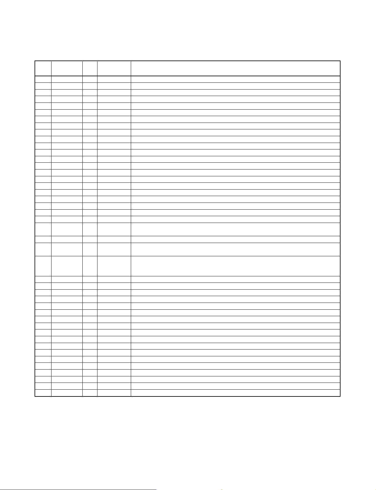
■ PIN Function table
Pin
Pin Name I/O
State after
Function
No. Reset
1 JITTC A — Jitter detection capacitor connection pin jitter detection capacitor connection pin
2 ADAVDD — — Servo A/D, D/A power supply pin
3 ADAVSS — — Servo A/D, D/A ground pin. Must be connected to 0V.••0V •••••ƒ•••
4 SLCO AO — Slice level control charge pump output pin
5 SLCIST AI — Slice level control charge pump current setting resistance connection pin
6 EFMIN I — RF signal input pin
7 RF AO ZHI RF signal output pin
8 RFVDD — — RF power supply pin
9 FE AO ZHI FE signal monitor pin
10 TEC AO — TE signal LPF capacitor connection pin
11 TE AO ZHI TE signal monitor pin
12 VREF AO RFVDD /2 VREF voltage output pin
13 REFI AI — VREF reference voltage monitor pin
14 TIN1 AI — E signal input pin
15 FIN1 AI — A+C signal input pin
16 FIN2 AI — B+D signal input pin
17 TIN2 AI F signal input pin
18 RFVSS — — RF ground pin. Must be connected to 0V.
19 LDD AO — Laser power control signal output pin
20 RFMON AO ZHI RF internal signal monitor pin
21 LDS AI • Laser power detection signal input pin
22 TEST I • Test input pin. Must be connected to 0V.
23 SBCK/FG I — Subcode read clock input pin / FG signal input pin
Set pin function with a command. When not used, connect to 0V.
24 DEFECT O L Defect signal monitor pin
25 V/PB O H Rough servo/phase control automatic switching monitor output pin. “H”: Rough
servo, “L”: Phase servo
26 FSEQ O L Synchronization signal detection output pin
“H” when synchronization signal detected from EFM signal and internally generated
synchronization signal match.
27 FOPWMF O L Focus PWM output pin
28 FOPWMR O L Focus PWM output pin
29 TRPWMF O L Tracking PWM output pin
30 TRPWMR O L Tracking PWM output pin
31 SPPWMF O L Spindle PWM output pin
32 SPPWMR O L Spindle PWM output pin
33 SLPWMF O L Thread PWM output pin
34 SLPWMR O L Thread PWM output pin
35 PWMCK O L PWM carrier frequency output pin
36 VSS — — Digital ground pin. Must be connected to 0V.
37 VDD1 — — Digital power supply pin
38 VDD3 — — Microcomputer I/F power supply pin
39 MONI1 O L Internal signal monitor pin 1
40 MONI2 O L Internal signal monitor pin 2
41 DOUT O • Digital OUT output pin (EIAJ format)
42 MONI3 O L Internal signal monitor pin 3
43 MONI4 O L Internal signal monitor pin 4
44 MONI5 O L Internal signal monitor pin 5
Page 24
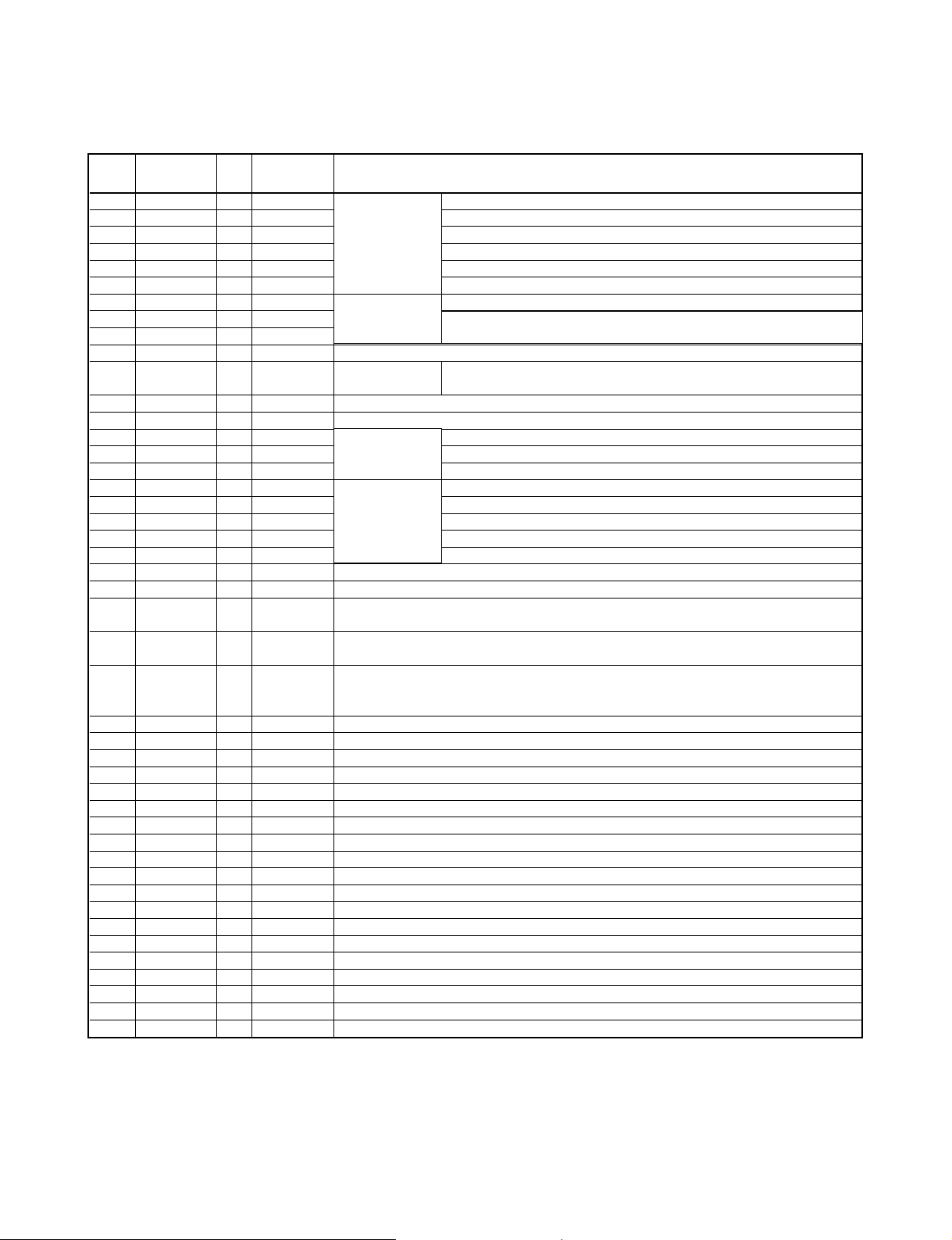
- 2-21 -
PinNo
Pin Name I/O
State after
Function
No. Reset
45 LVDD — — L channel power supply pin
46 LCHO AO LVDD /2 L channel output pin
47 LVSS — — L channel ground pin. Must be connected to 0V.
48 RVSS — — R channel ground pin. Must be connected to 0V.
49 RCHO AO LVDD /2 R channel output pin
50 RVDD — — R channel power supply pin
51 XVDD — — Crystal oscillation power supply pin
52 XOUT O Oscillation
53 XIN I Oscillation
54 FSX/16MIN I/O Input mode 7.35 kHz synchronization signal output pin, or DF/DAC external clock input pin
55 XVSS — — For crystal Crystal oscillation ground pin. Must be connected to 0V.
oscillation
56 16MOUT O CLK output 16.9344 MHz output pin
57 C2F/EFLG O H C2 flag output pin (in reset). C1, C2 correction monitor pin
58 LRSY O L L/R clock output pin
59 DATACK O L Bit clock output pin
60 DATA O L L/R channel data output pin
61 CE I — Chip enable signal input pin
62 CL I — Data transfer clock input pin
63 DI I — Data input pin
64 DO O (H) Data output pin (Nch open-drain output)
65 WRQB O H Interrupt signal output pin
66 RESB I — LC78647NT IC reset input pin. Drive to “L” level at power-on.
67 DRF O L Focus ON detection pin
68 WOK/
I —
DRAM write enable signal input. “H”: Write enabledL/R clock input pin
ASLRCK
69 OVF/
I/O —
DRAM write suspension Bit clock input pin. ASDACK input mode after reset
ASDACK
70
CNTOK/
I/O —
Data connection point detection completed signal
ASDFIN
L/R channel data input pin. ASDFIN input mode after reset
Bit clock input pin. ASDACK input mode after reset
71 VSS — — Digital ground pin. Must be connected to 0V.
72 OEB O H DRAM control signal output pin
73 CASB O H DRAM control signal output pin
74 RAMD2 I/O — DRAM data I/O pin
75 RAMD3 I/O — DRAM data I/O pin
76 MVSS — — DRAM I/F ground pin. Must be connected to 0V.
77 MVDD — — DRAM I/F power supply pin
78 RAMD0 I/O — DRAM data I/O pin
79 RAMD1 I/O — DRAM data I/O pin
80 WEB O H DRAM control signal output pin
81 RASB O H DRAM control signal output pin
82 A11 O L DRAM address output pin
83 A10 O L DRAM address output pin
84 A9 O L DRAM address output pin
85 A8 O L DRAM address output pin
86 A7 O L DRAM address output pin
87 A6 O L DRAM address output pin
88 A5 O L DRAM address output pin
89 A4 O L DRAM address output pin
16.9344 MHz resonator connection pins
For L
channel
audio
For crystal
oscillation
For digital
data output
microcompu
ter interface
Page 25
- 2-22 -
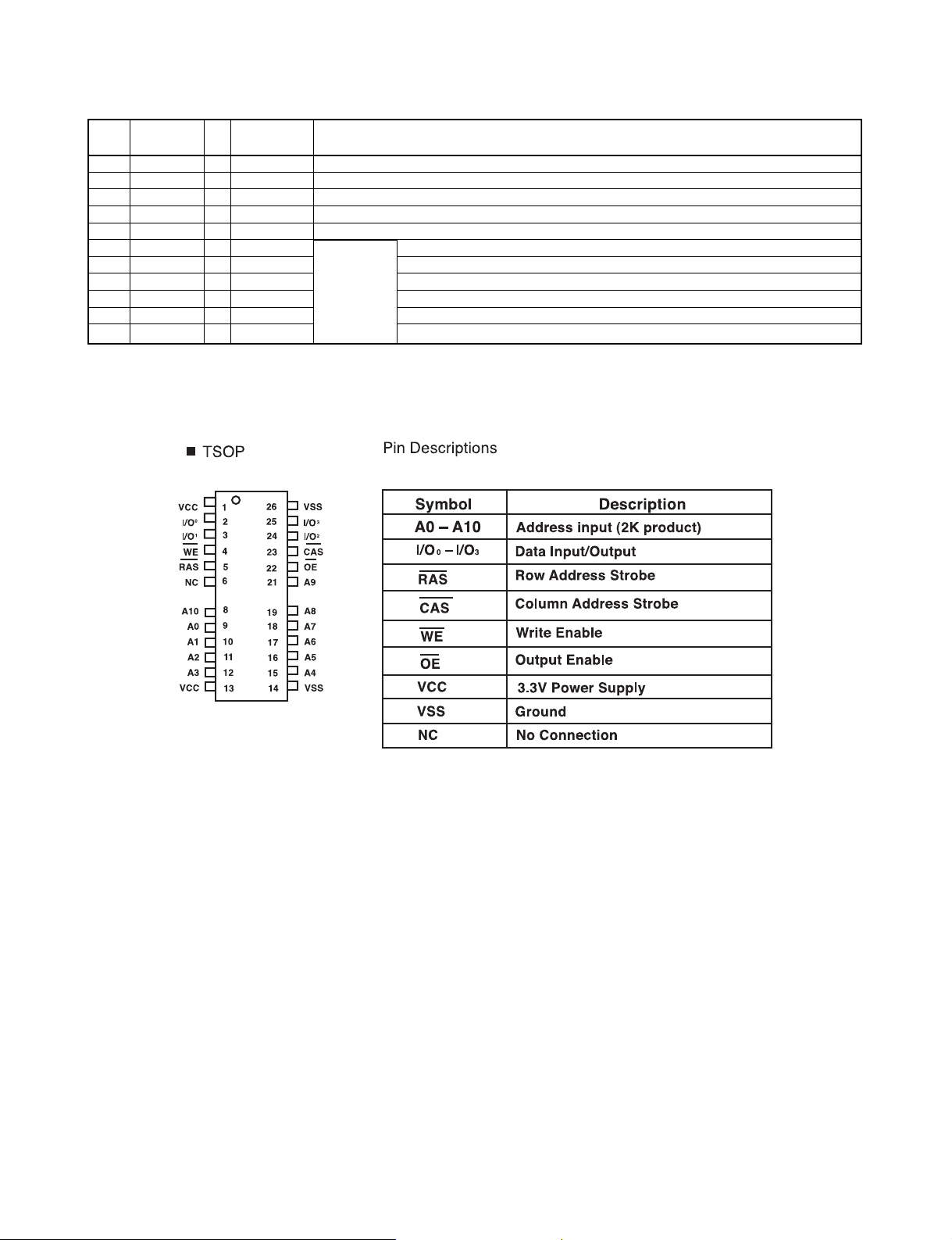
Pin Pin Name I/O State after Function
No. Reset
90 A0 O L DRAM address output pin
91 A1 O L DRAM address output pin
92 A2 O L DRAM address output pin
93 A3 O L DRAM address output pin
94 VDD2 — — Digital power supply pin
95 VVSS — — Built-in VCO ground pin. Must be connected to 0V.
96 PDO1 O — Built-in VCO control phase comparison output pin 1
97 PDO2 O Input mode Built-in VCO control phase comparison output pin 2
98 PCKIST AI — PDO1, PDO2 output current setting resistance connection pin
99 FR AI — Built-in VCO control frequency range setting resistance connection pin
100 VVDD — — Built-in VCO power supply pin
For PLL
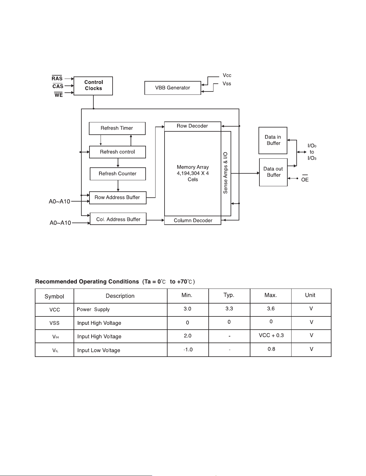
■ IC502 A42L2604V
Page 26
- 2-23 -
■ Block Diagram
Page 27
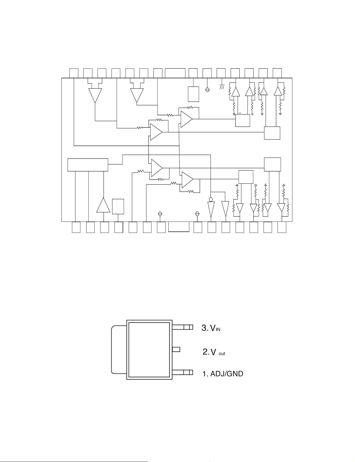
- 2-24 -
■ IC503 BA5810FP
28
27
26
25 24
23
22
21 20 19 18 17 16 15
1234 5
6
7 8 9 1011121314
++–+–
+–
+–
+–
7.5k
7.5k
7.5k
7.5k
LOADING PRE
FWE REV
X3
POWER
SAVE
16k
16k
16k
16k
PREVCC
(PRE. LODING)
PREVCC12
(CH1. CH2)
CD1~
CB4
MUTE
POWVCC34
(CH3, CH4)
10k
10k
10k 10k
10k
10k
10k
10k
LEVEL
SHIFT
LEVEL
SHIFT
LEVEL
SHIFT
LEVEL
SHIFT
10k
10k
10k
10k
10k
10k
■ IC504 AMC1117
Page 28
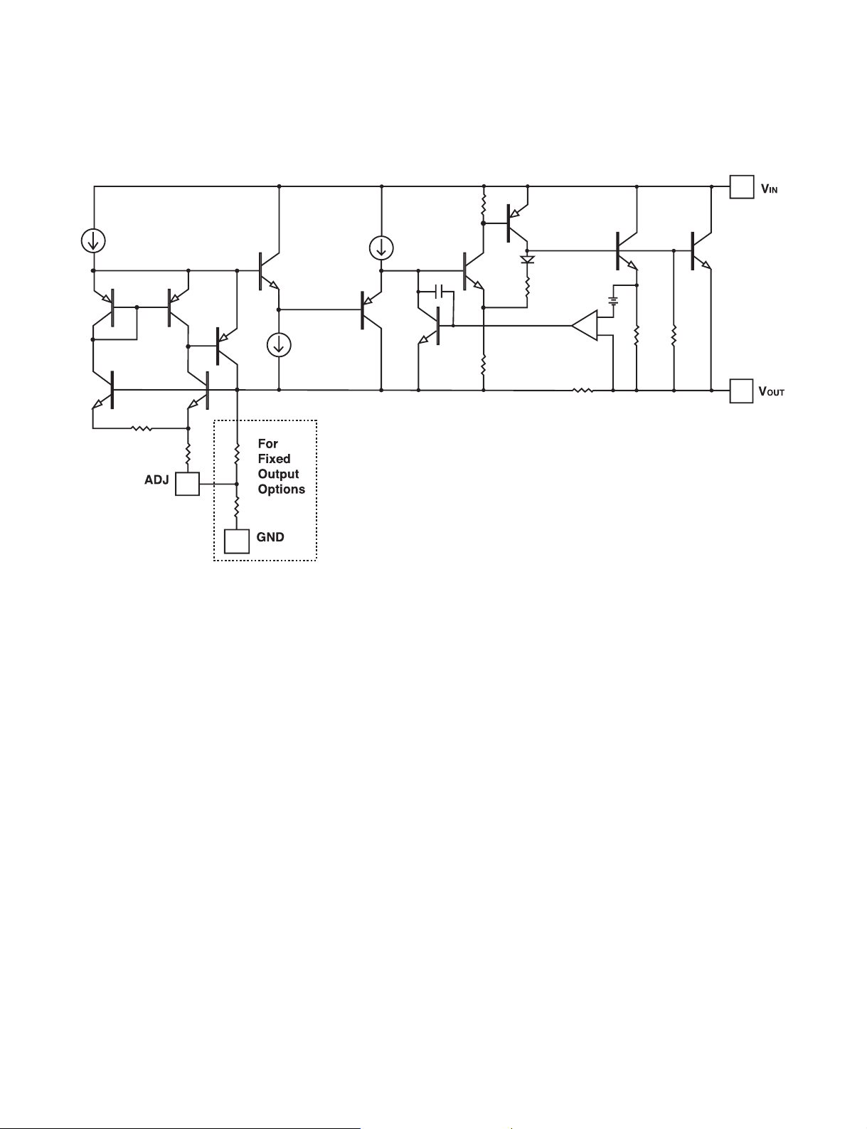
- 2-25 -
■ BLOCK DIAGRAM
Page 29
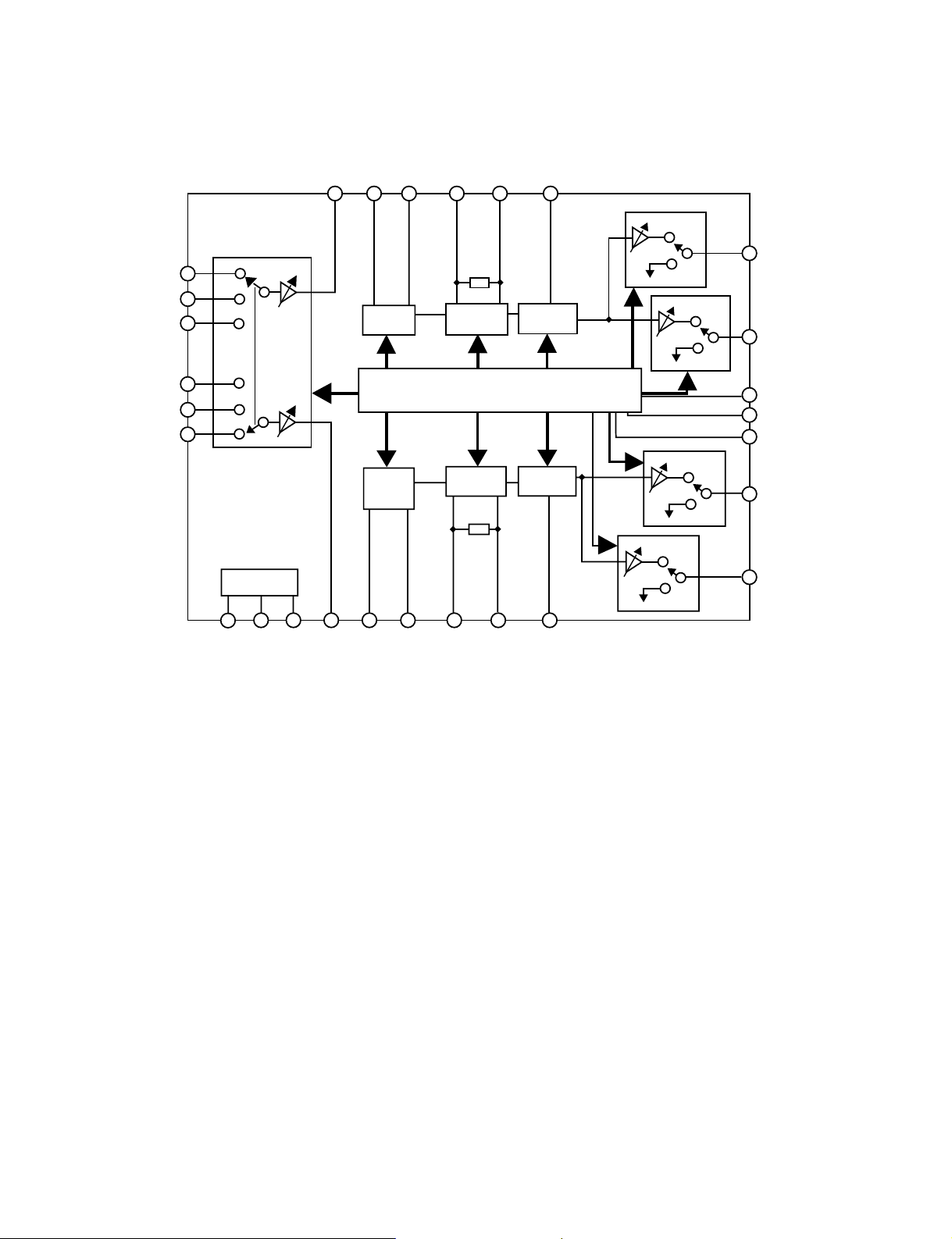
- 2-26 -
■ IC601 PT2313L
RB
RB
TREB_RBIN_RBOUT_RLOUDRINROUTREFAGNDVDD
RIN1
RIN1
RIN2
RIN2
RIN3
RIN3
LIN3
LIN3
Input
Selector
& Gain
Control
LIN2
LIN2
LIN1
LOUT LIN LOUD_L BOUT_L BIN_L TREB_L
LFOUT
Mute
Mute
Mute
Mute
Speaker
ATT
Speaker
ATT
Speaker
ATT
Speaker
ATT
LROUT
CLK
DATA
DGND
RFOUT
RROUT
LIN1
2
11
10
9
13
14
15
17 16 12 19
18
4
25
23
28
27
26
24
22
31 7 6 8 21
20
5
Supply
Bass
Serial Bus Decoder & Latches
Bass
Treble
Treble
Voume
&
Loudness
Voume &
Loudness
Page 30
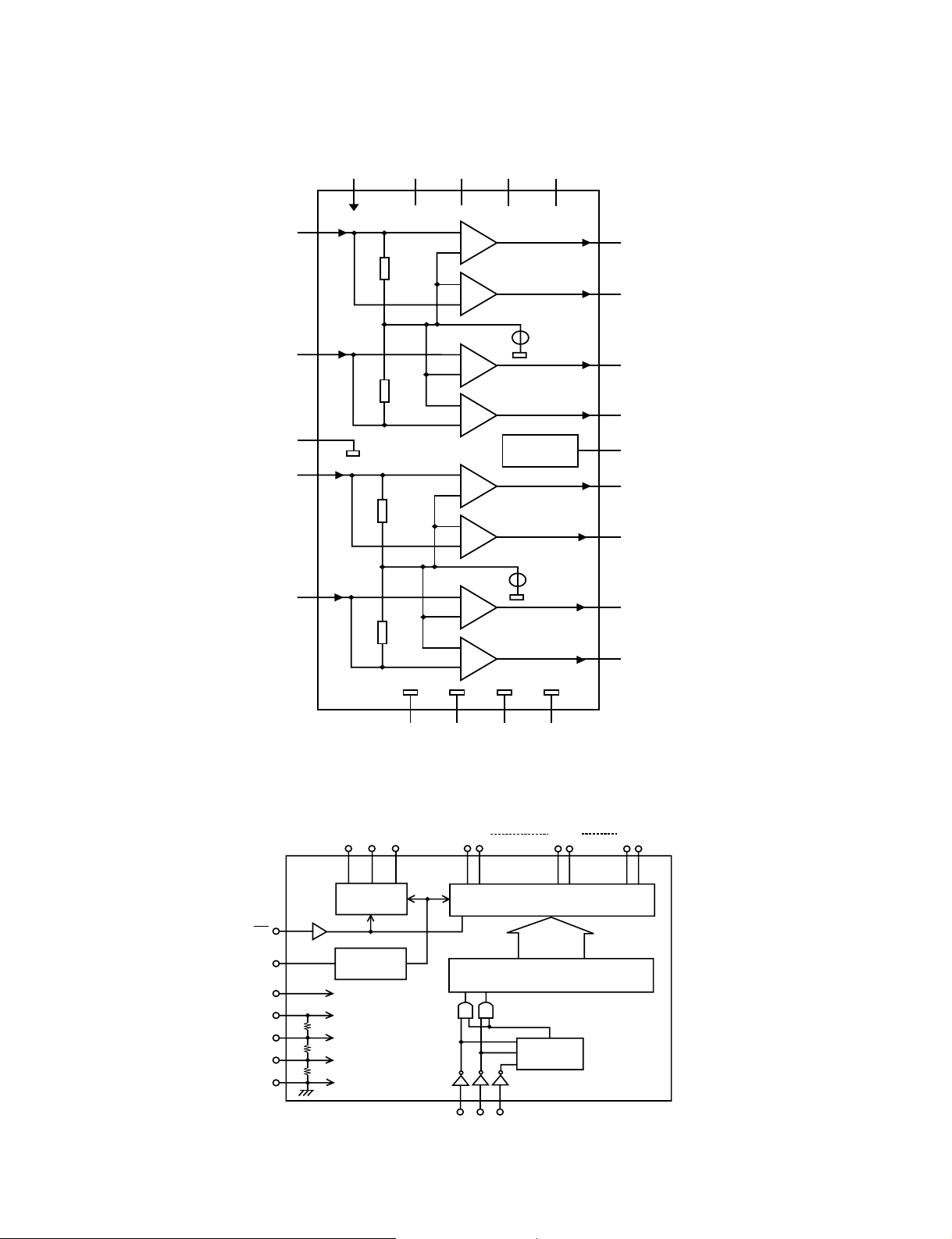
- 2-27 -
■ IC801 TDA8571J
+
-
+
-
+
-
+
-
+
-
+
-
+
-
+
-
PGND1 PGND2 PGND3 PGND4
MGG153
OUT4
-
OUT4+
OUT3+
DIAGNOSTIC
OUT2+
V
OUT1+
OUT3
-
OUT2
-
OUT1
-
21
20
22
19
17
9
5
7
4
2
23 16
10
11
12
13
14
30 K•
30 K•
30 K•
30 K•
IN1
MODE
IN2
SGND
IN3
IN4
8 1 15
186
3
ref
V
P1
V
P2
V
P3
V
P4
V
ref
V
DIAG
■ IC901 PT6523
V
SS
V2
LCD
V1
LCD
V
V
LCD
OSC
Common
driver
Segment driver & latch
Shift register
Clock
generator
Address
detector
COM3
DI
CL
CE
COM2
COM1
S35
ZZ
ZZ ZZ ZZ
S34
S9
S8/P8
S2/P2
S1/P1
INH
DD
Page 31
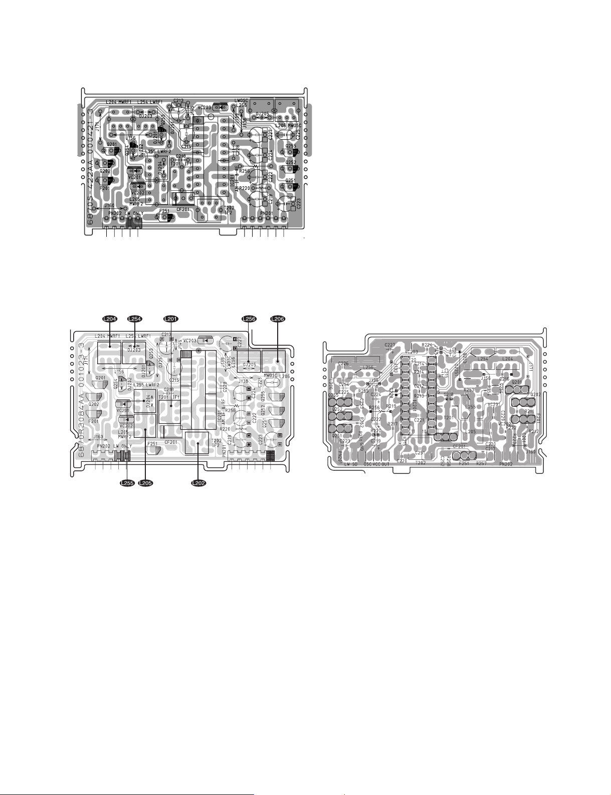
- 2-45 -
5. RF P.C. BOARD(OLD P.C. BOARD)
(NEW RF P.C. BOARD)
(TOP VIEW)
(BOTTOM VIEW)
Page 32
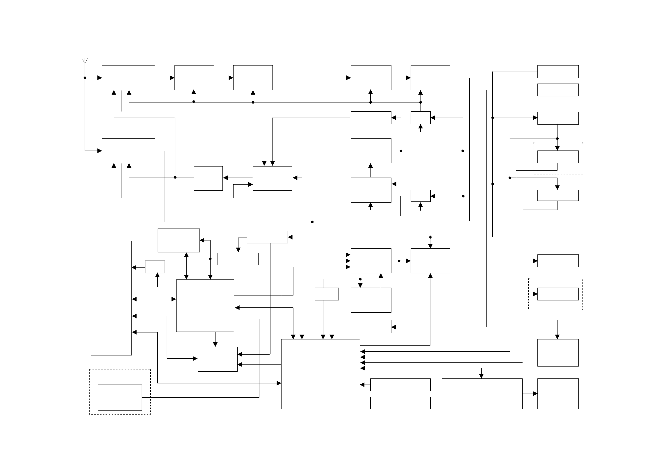
2-29 2-30
❏ BLOCK DIAGRAM
TU101 Q101,CF102 IC101 IC102 IC103
VT FM Vcc FM Vcc FM Vcc FM Vcc FM Vcc
Vdd Q807
TU201 FM ON *OPTION
Q109,110 FM OSC
AM Vcc VT Q805
IC104
AM OSC
PWR ON AM ON Q803,Q804
IC502 Q505,Q506,Q507
IC504 IC601
LD S/W MUTE IC801
IC501 *OPTION
LEVEL DET
ACC DET
IC503
*OPTION
FM F/ END
IF Filter &
Amp
IF IC
[LA1140]
NC IC
[KIA6010]
MPX IC
[LA3430M]
AM TUNER
LPF1
PLL IC
[KIC9256P]
Q112
Q203
9.4V Reg
Q802
PWR 14V
Q808,Q809
4.7V ZD102
CD MECHA
TN-2001-005
D-RAM IC
[A43L2604V]
DSP IC
[LC78647NT]
BTL DRIVER
IC
[BA5810FP]
E/Vol IC
[PT2312L]
POWER IC
[TDA8571]
AF Amp
[Q601,Q602]
CDC
u-COM
IC401
[LC875700A]
B/UP
ACC
Q806
SPK
LINE OUTD601
5V Reg
LED Flash
RESET
DIODE MATRIX
LCD DRIVER IC
IC901
[PT6523]
KEY IN1/2
LCD
Back Light
[LD901~925]
3.3V Reg
7.5V Reg
Q501
Page 33
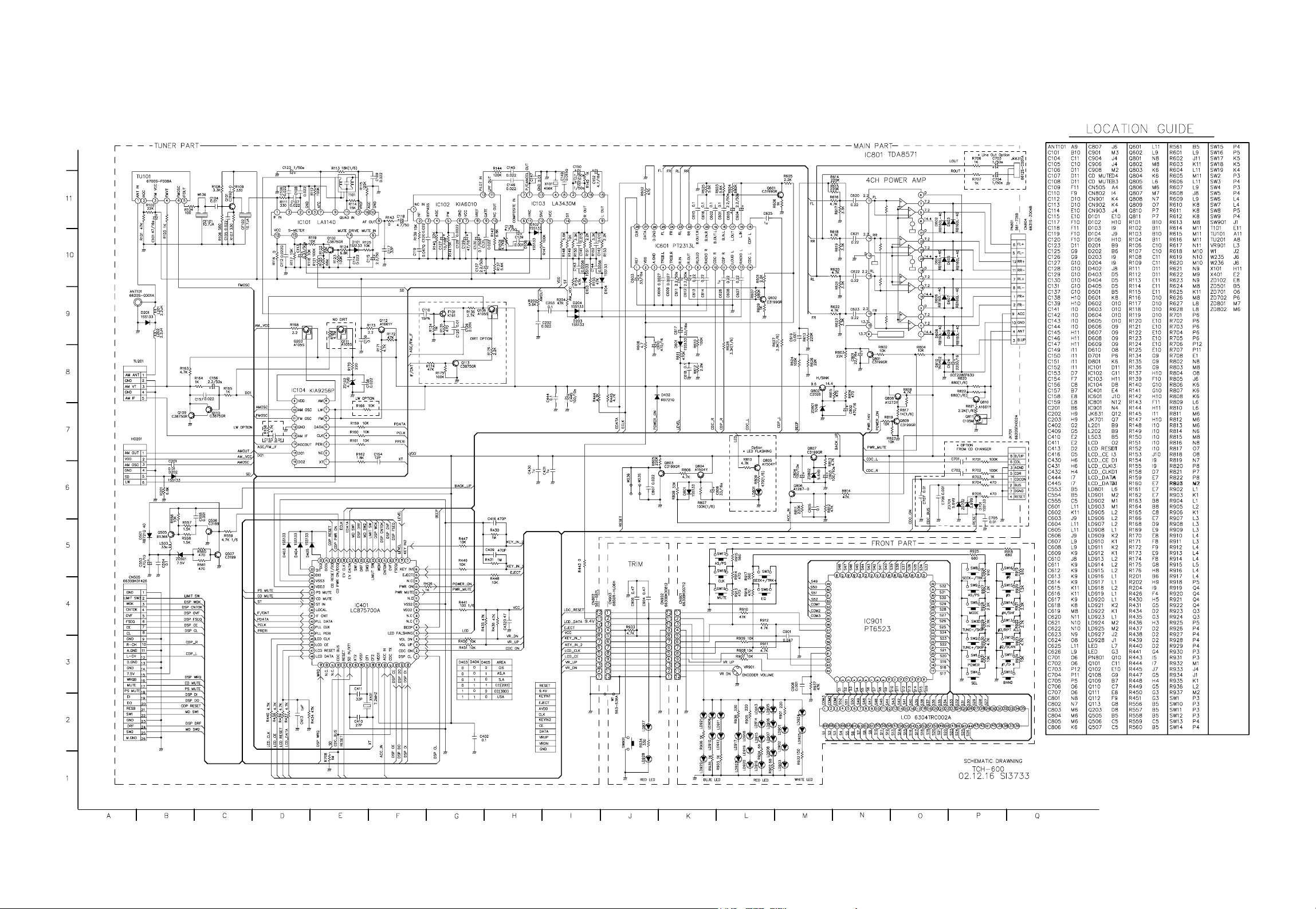
❏ MAIN SCHEMATIC DIAGRAM
2-31 2-32
Page 34
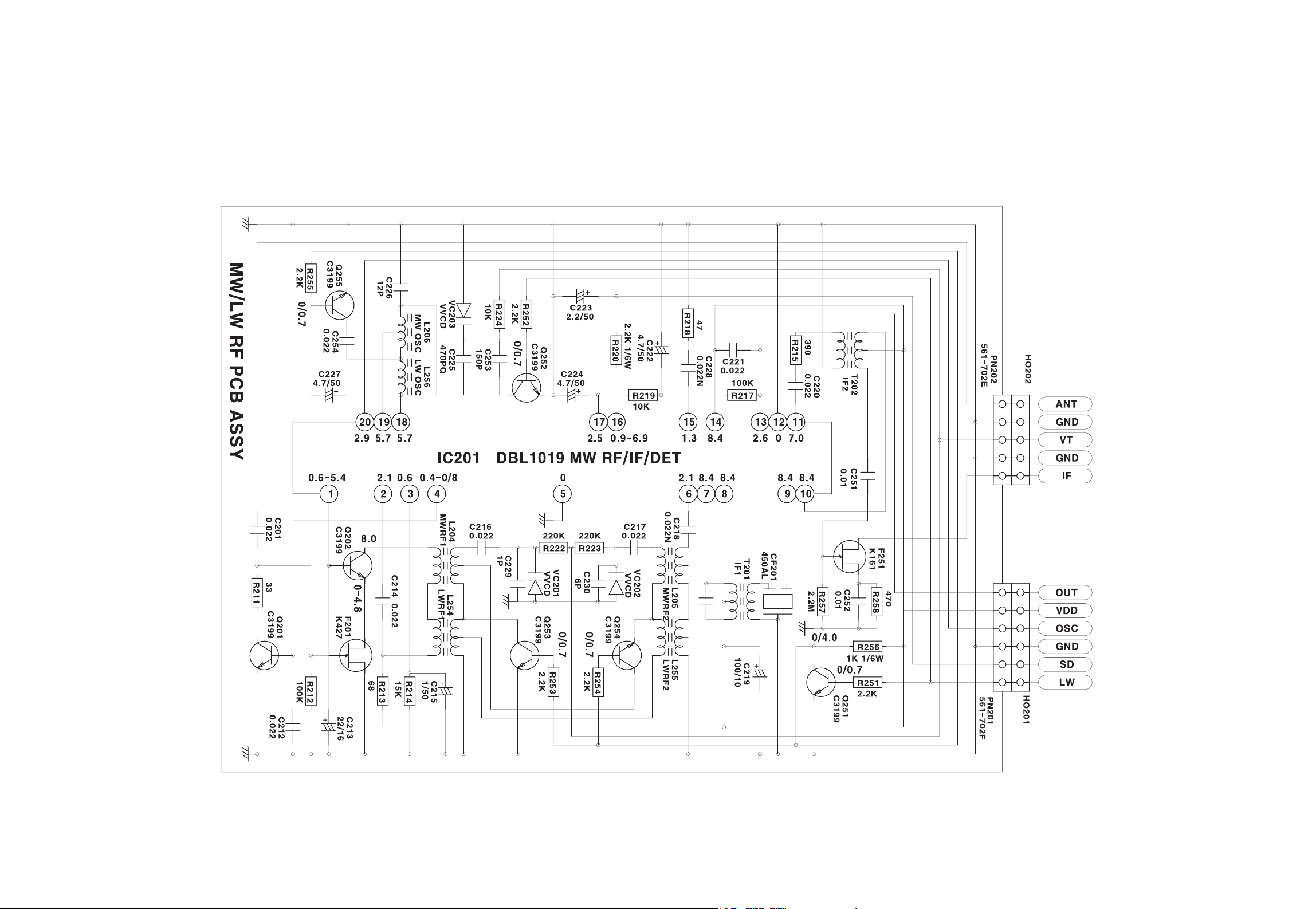
2-33 2-34
❏ MW/LW RF SCHEMATIC DIAGRAM
Page 35
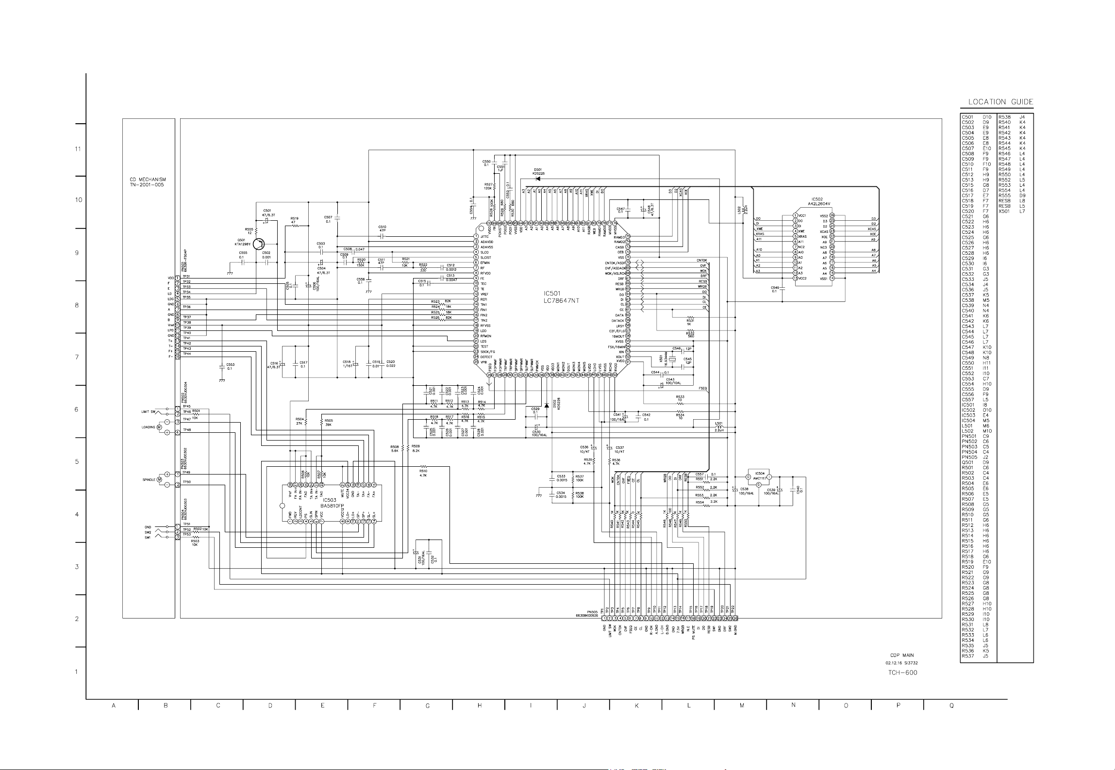
2-35 2-36
❏ CDP SCHEMATIC DIAGRAM
Page 36
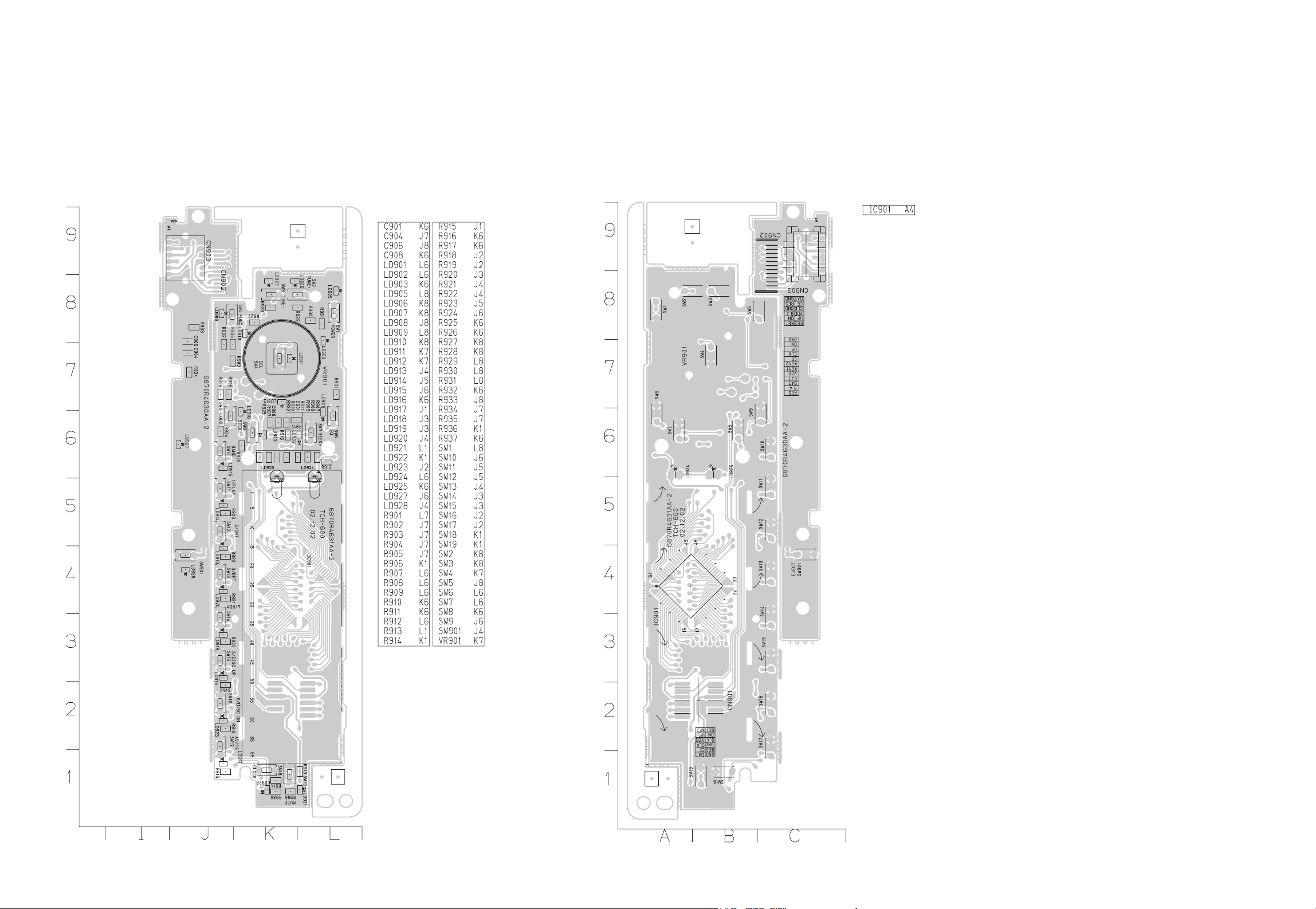
2-37 2-38
❏ PRINTED CIRCUIT DIAGRAM
1. FRONT P.C. BOARD
(COMPONENT SIDE)
2. FRONT P.C. BOARD
(SOLDER SIDE)
Page 37
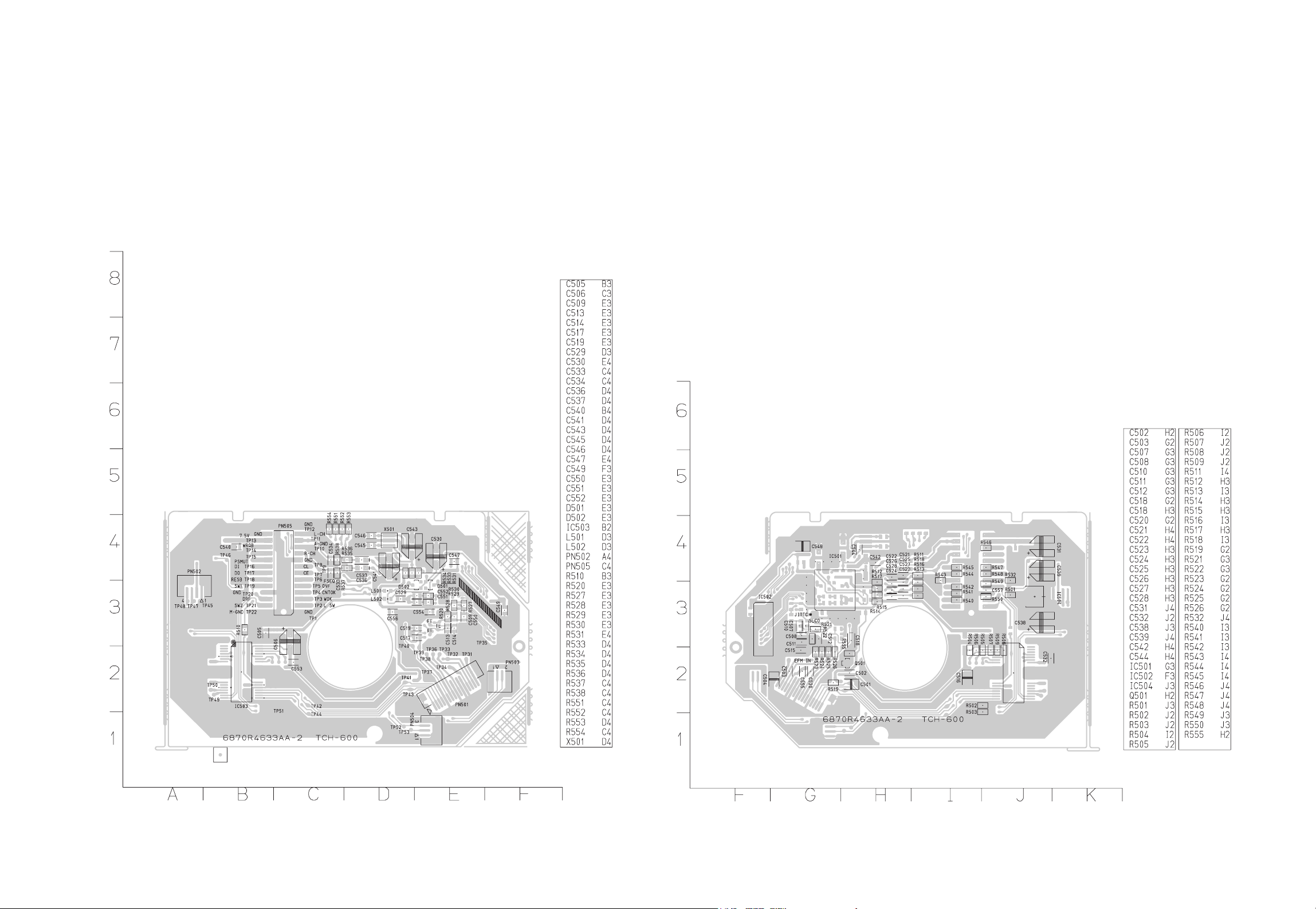
2-39 2-40
3. CDP BOARD(SOLDER SIDE) 3. CDP BOARD(COMPONENT SIDE)
Page 38
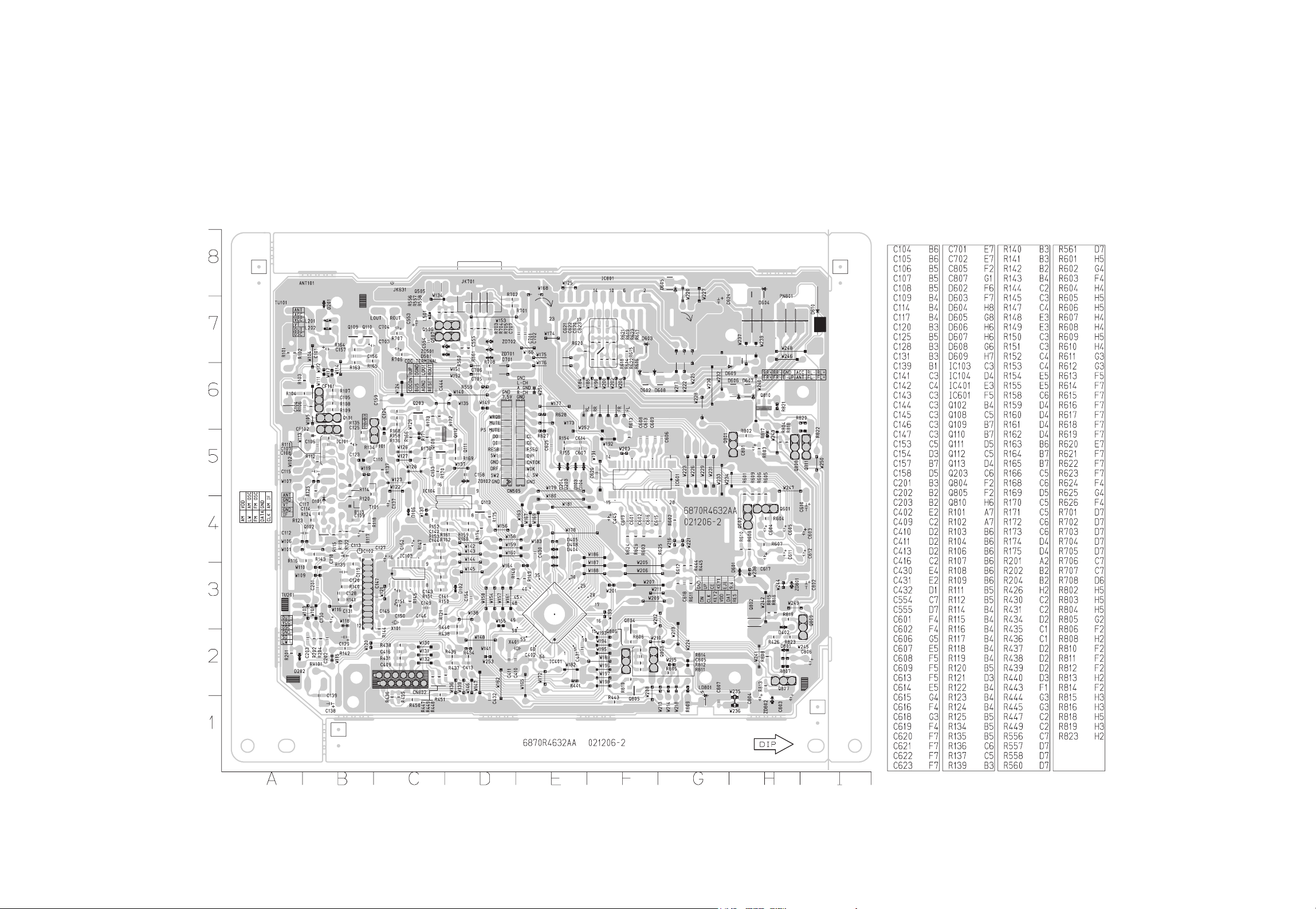
2-41 2-42
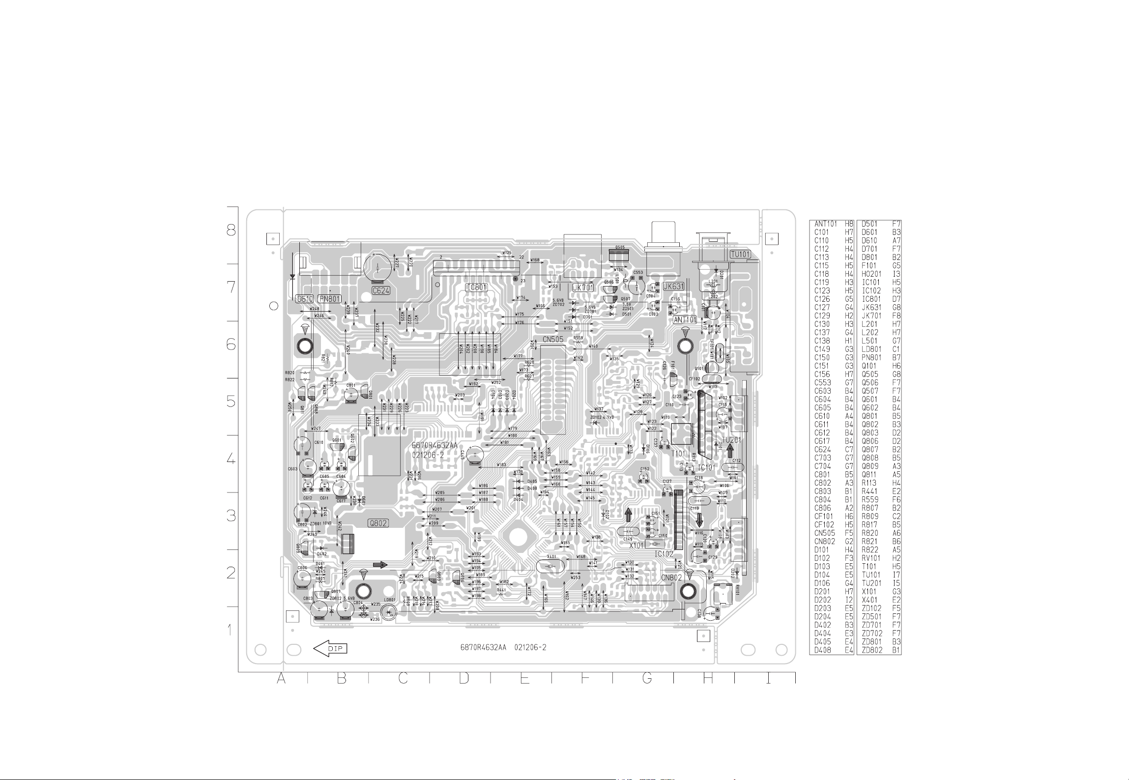
4. MAIN P.C. BOARD(SOLDER SIDE)
Page 39
2-43 2-44
4. MAIN P.C. BOARD(COMPONENT SIDE)
Page 40
3-1 3-2
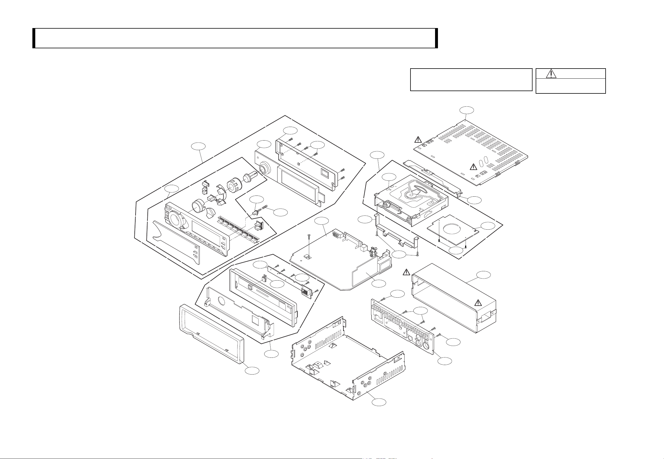
■ EXPLODED VIEW
301
320
441
447
441
301
281
A44
A43
278
457
A46
A47
285
441
A00A
286
330
455
302
A42
A41
A40
275
274
A00
A00B
450
CAUTION
Exposed blade will cause
severe injury
SECTION 3. CABINET MAIN CHASSIS & MECHANISM
NOTE) Refer to “SECTION 4 REPLACEMENT
PARTS LIST” in order to look for the
part number of each part.
 Loading...