

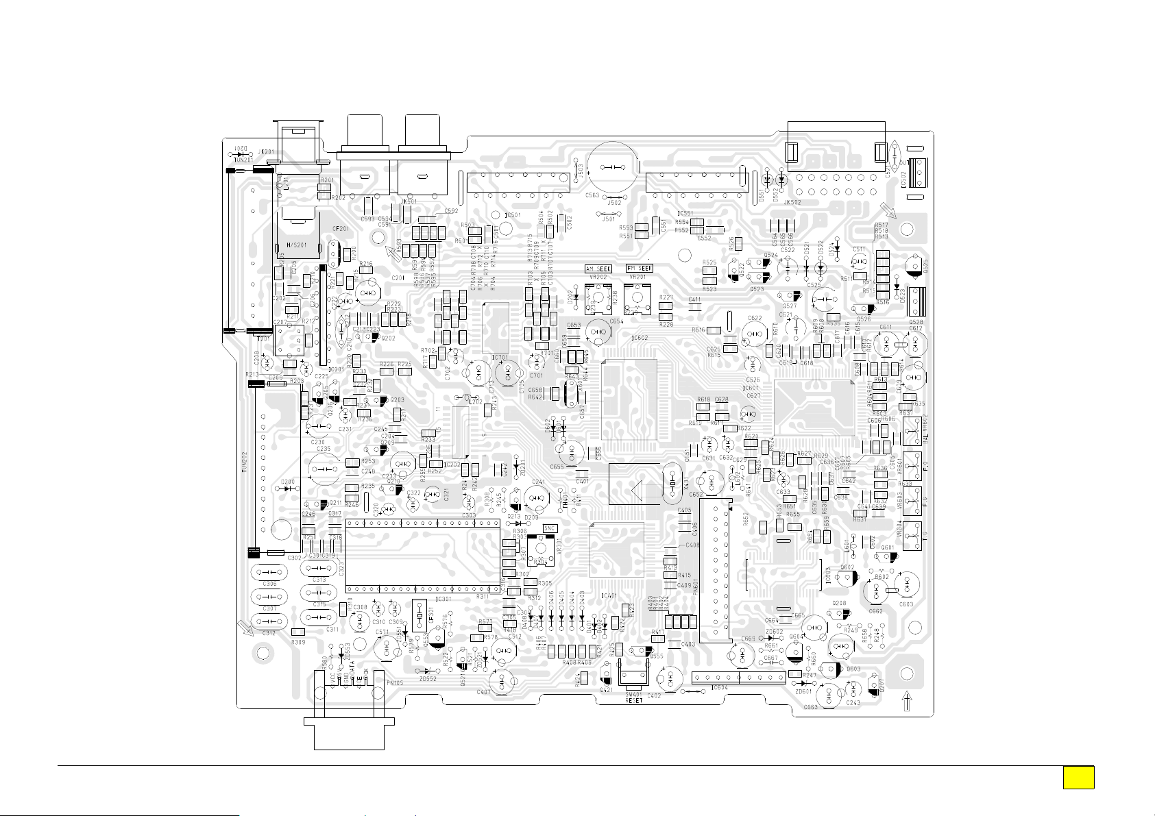
Page 1
q
MAIN SECTION
Ú
TOP VIEW
Drawing No. : 6870S-32KAA
1
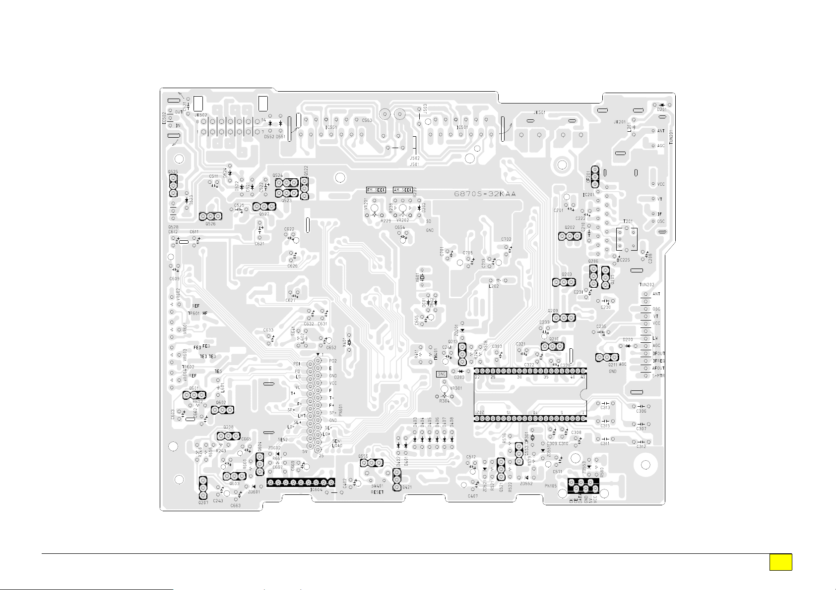
Page 2
q
MAIN SECTION
Ú
BOTTOM VIEW
Drawing No. : 6870S-32KAA
2
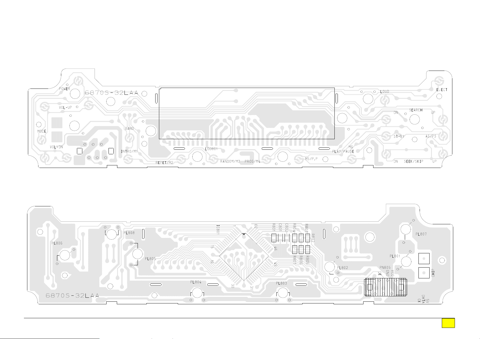
Page 3
q
FRONT SECTION
Ú
TOP VIEW
Drawing No. : 6870S-32LAA
Ú
BOTTOM VIEW
1
Page 4
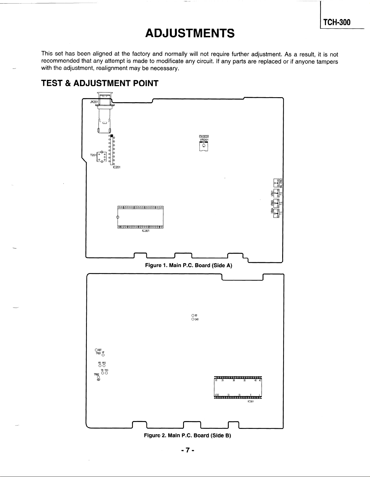
TCH-300
ADJUSTMENTS
This set has been aligned at the factory and normally will not require further adjustment. As a result, it is not
recommended that any attempt is made to modificate any circuit. If any parts are replaced or if anyone tampers
-
with the adjustment, realignment may be necessary.
TEST & ADJUSTMENT POINT
.
L
t ,
I
T201 O ,"
\ 0
l_
0 0
J
IC201
I
IFM]
VR201
6
El
/
-
Figure 1. Main PC. Board (Side A)
r
ORE
TP601 5
FEI FE0
00
TEI TEO
TPGM O"
0
REF
OS0
OGND
1
Figure 2. Main P.C. Board (Side B)
Page 5
TCH-300 1
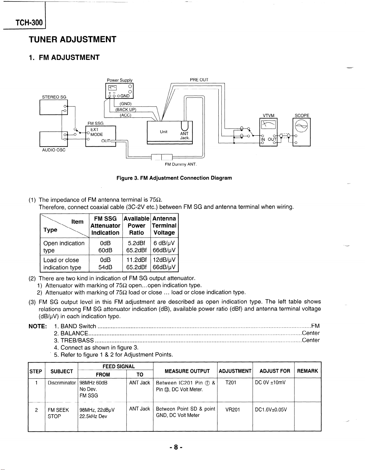
TUNER ADJUSTMENT
1. FM ADJUSTMENT
-
Power Supply
- 01
STEREO SG
FM SSG
AUDIO OSC
1-n
FM Dummy ANT.
Figure 3. FM Adjustment Connection Diagram
(1) The impedance of FM antenna terminal is 7X&.
Therefore, connect coaxial cable (3C-2V etc.) between FM SG and antenna terminal when wiring.
\
Open indication OdB
type
Load or close OdB
indication type 54dB
(2) There are two kind in indication of FM SG output attenuator.
1) Attenuator with marking of 75Q open...open indication type.
2) Attenuator with marking of 75Q load or close . . . load or close indication type.
(3) FM SG output level in this FM adjustment are described as open indication type. The left table shows
relations among FM SG attenuator indication (dB), available power ratio (dBf) and antenna terminal voltage
(dB/uV) in each indication type.
NOTE:
1. BAND Switch
2. BALANCE
3. TREB/BASS
4. Connect as shown in figure 3.
- 5. Refer to figure 1 & 2 for Adjustment Points.
FM SSG Available Antenna
Attenuator
Indication Ratio Voltage
60dB
. . . . . . . . . . . . . . . . . . . . . . . . . . . . . . . . . . . . . . . . . . . . . . . . . . . . . . . . . . . . . . . . . . . . . . . . . . . . . . . . . . . . . . . . . . . . . . . . . . . . . . . . . . . . . . . . . . . . . . . . ..........
. . . . . . . . . . . . . . . . . . . . . . . . . . . . . . . . . . . . . . . . . . . . . . . . . . . . . . . . . . . . . . . . . . . . . . . . . . . . . . . . . . . . . . . . . . . . . . . . . . . . . . . . . . . . . . . . . . . . . . . . ..........
. . . . . . . . . . . . . . . . . . . . . . . . . . . . . . . . . . . . . . . . . . . . . . . . . . . . . . . . . . . . . . . . . . . . . . . . . . . . . . . . . . . . . . . . . . . . . . . . . . . . . . . . . . . . . . . . . . . . . . . . ....~.
Power Terminal
52dBf 6 dB/pV
652dBf 66dB/uV
11.2dBf 12dB/uV
65.2dBf 66dB/uV
PRE OUT
11
-II
VTVM SCOPE
I II
/
.
FM
Center
Center
STEP SUBJECT
1 Discriminator 98MHz 60dB
No Dev.
FM SSG
FM SEEK 98MHz, 22dBpV
2
STOP
225kHz Dev
FEED SIGNAL
FROM TO
ANTJack Between IC2Ol Pin 0 &
ANT Jack Between Point SD & point
MEASURE OUTPUT ADJUSTMENT ADJUST FOR REMARK
T201
Pin 0, DC Volt Meter.
VR201 DC1.6V+O.O5V
GND, DC Volt Meter
DC OV +lOmV
-8-
Page 6
--
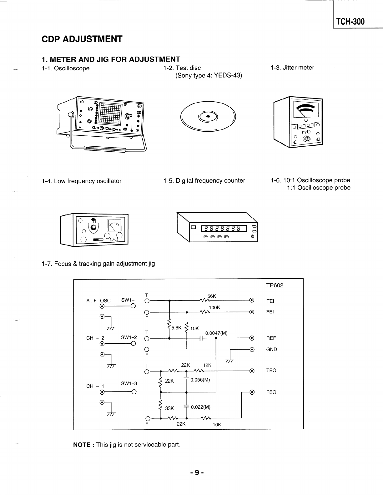
CDP ADJUSTMENT
1. METER AND JIG FOR ADJUSTMENT
l-l. Oscilloscope
1-2. Test disc
TCH-300
1-3. Jitter meter
(Sony type 4: YEDS-43)
1-4. Low frequency oscillator
-
1-7. Focus & tracking gain adjustment jig
A. F OSC
04
0 0 0 F
CH I - 2 SWI-2 1 I
oe
0 0 F
SWI-1 0
0
0
1-5. Digital frequency counter
T
T
T
w
22K
56K
1 OOK
0.0047(M)
12K
\ I
0
J
1-6. 10: 1 Oscilloscope probe
1: 1 Oscilloscope probe
TP602
TEI
FEI
REF
GND
TEO
CH - 1
F
NOTE : This jig is not serviceable part.
22K
-9-
10K
0
FE0
s
Page 7
--
_
TCH-300
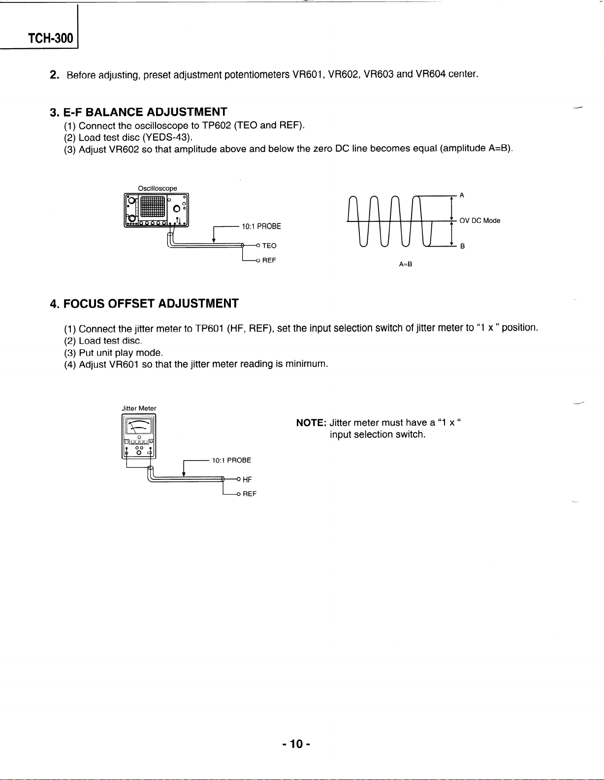
2. Before adjusting, preset adjustment potentiometers VR601, VR602, VR603 and VR604 center.
3. E-F BALANCE ADJUSTMENT
(1) Connect the oscilloscope to TP602 (TEO and REF).
(2) Load test disc (YEDS-43).
(3) Adjust VR602 so that amplitude above and below the zero DC line becomes equal (amplitude A=B).
Oscilloscope
k REF
4. FOCUS
(1)
(2)
(3)
(4)
OFFSET ADJUSTMENT
Connect the jitter meter to TP601 (HF, REF), set the input selection switch of jitter meter to “1 x ” position.
Load test disc.
Put unit play mode.
Adjust VR601 so that the jitter meter reading is minimum.
Jitter Meter
NOTE: Jitter meter must have a “1 x
input selection switch.
A=B
A
OV DC Mode
B
“
-IO-
Page 8
TCH-300
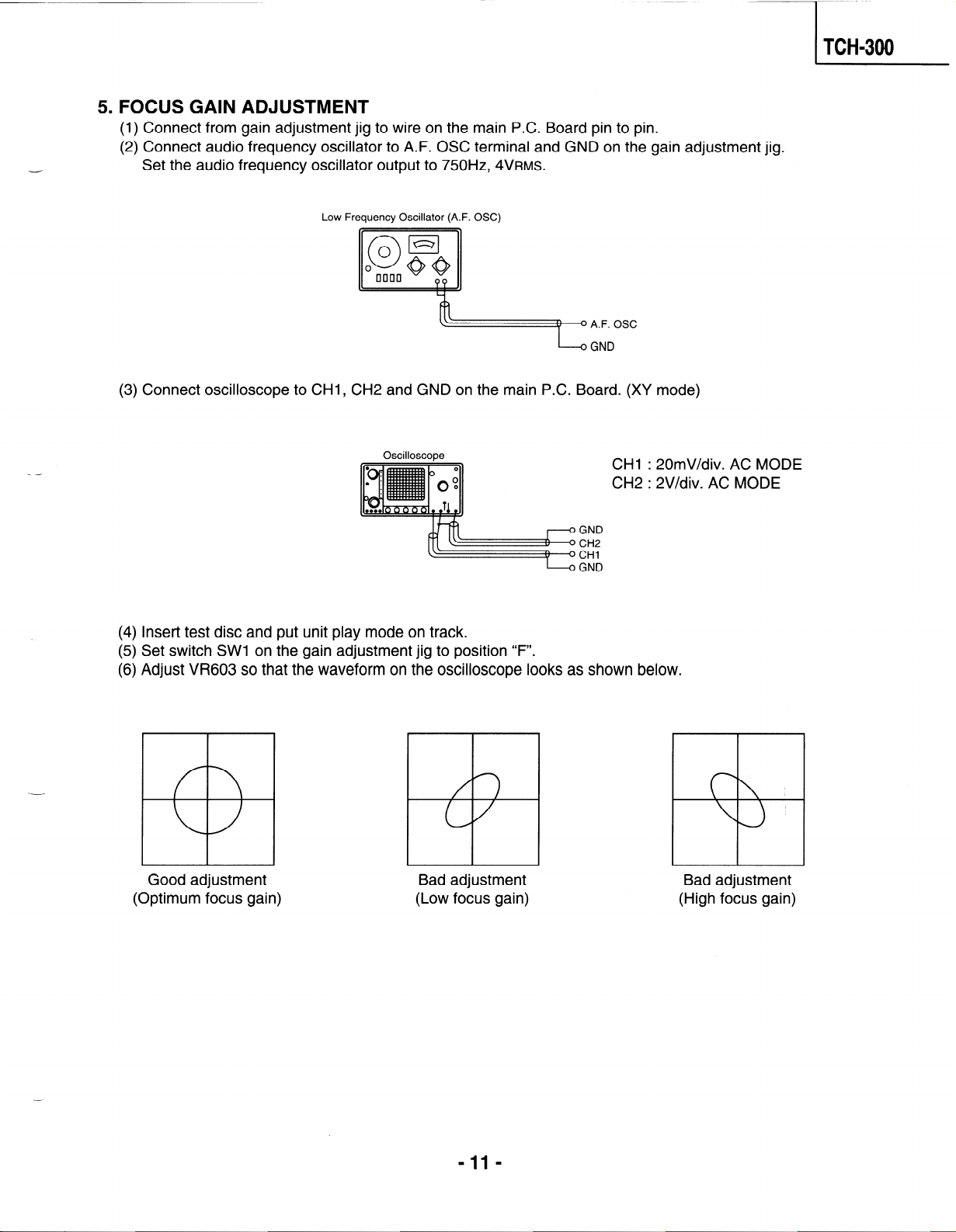
5. FOCUS GAIN ADJUSTMENT
(1) Connect from gain adjustment jig to wire on the main P.C. Board pin to pin.
(2) Connect audio frequency oscillator to A.F. OSC terminal and GND on the gain adjustment jig.
-
Set the audio frequency oscillator output to 750Hz, ~VRMS.
Low Frequency Oscillator (A.F. OSC)
@@O A.F. OSC
L
GND
(3) Connect oscilloscope to CHI, CH2 and GND on the main P.C. Board. (XV mode)
-----
Oscilloscope
I-O GND
Insert test disc and put unit play mode on track.
(4)
Set switch SW1 on the gain adjustment jig to position
(5)
Adjust VR603 so that the waveform on the oscilloscope looks as shown below.
(6)
Good adjustment
(Optimum focus gain)
Bad adjustment
(Low focus gain)
“F”.
CHI : 20mV/div. AC MODE
CH2 : 2V/div. AC MODE
Bad adjustment
(High focus gain)
-ll-
Page 9
( TCH-300
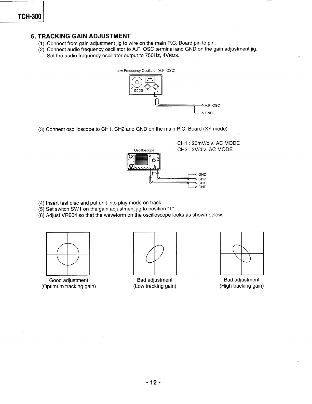
6. TRACKING GAIN ADJUSTMENT
Connect from gain adjustment jig to wire on the main P.C. Board pin to pin.
(1)
Connect audio frequency oscillator to A.F. OSC terminal and GND on the gain adjustment jig.
(2)
Set the audio frequency oscillator output to 750Hz, ~VRMS.
Low Frequency Oscillator (A.F. OSC)
Connect oscil
Insert test disc and put unit into play mode on track.
(4)
Set switch SW1 on the gain adjustment jig to position
(5)
Adjust VI3604 so that the waveform on the oscilloscope looks as shown below.
(6)
I oscope to CHI, CH2 and GND on the main P.C. Board (XV mode)
CHI : 20mV/div. AC MODE
Oscilloscope
CH2 : 2V/div. AC MODE
“T”.
(Optimum tracking gain)
(Low tracking gain)
-12-
Bad adjustment
(High tracking gain)
Page 10

CD PART
c
CD Function Select
TCH-300
TROUBLESHOOTING
Is power turned ON?
I
YES
I
-
Does initial reading occur?
1
I
YES
NO
NO
m Check power supply circuitry.
.- .
w Check laser circuitry.
.
+ Check focusing circuitry.
w Check disc.
$
Can disc be played?
.
YES
NO
w Check tracking servo circuitry.
Is audio output supplied?
YES
I
OK
NO
- 27 -
Check Audio circuitry.
Page 11

TCH-300
(1) If display LCD lighting is not normal
CD Function Select
I
Do display LCD then light?
(WITHOUT DISC)
I
NO
Check voltage in the power
* supply circuitry.
I
YES
1
Is u-COM IC401 reset circuit
normal? Pin @
YES
I
Is u-COM IC401 C.L.K
terminal Pin @ (OSC)
input?
NO
NO
Reset circuit defective.
Surrounding circuit defective.
C405, C406 defective.
X401 defective.
about 0.25ysec w
YES
I
I
Is IC401 8, @ output
waveform normal?
YES
1
Is IC401 Pin @ output
waveform normal?
YES
NO
NO
Pattern defective.
Pattern defective.
- 28 -
Display defective.
Page 12

(2) If initial reading is not carried out (with Disc)
ITCH-300
Does disc motor rotate?
YES
Is RF wave
output?
RF
NO op.erating?
- Is the lower
1
Is tracking servo
envelope of RF
waveform flat?
YES
Is IC401 Pin @output
waveform normal?
Ic4” @%6-j DOOR CLOSE
YES
I
Does laser light?
Is signal output
at TEI?
NO
YES
NO
1
NO
NO
Leaf SW contact defective.
Connector defective.
Pattern short.
)8
Is signal
output,
at IC601
Pin @?
YES
- defective
NO
IC601 defective.
Connector
defective.
Pick-up defec-
tive.
Pattern
.
Is rotation normal?
Is there any irregularity in
frequency?
YES
1
Is HF signal normal without
dropout?
YES
I
Is signal output at tracking output
IC601 Pin @?
IC601 Pin @waveform
YES 1
Does IC602 Pin @(LKFS) as
figure?
NO
NO
NO
Disc initial reading damaged
w or defective.
IC601
defective.
Pick-up
defective.
Connector
defective.
- 29 -
w Disc defective.
Page 13

When laser does not light.
I
Is below signal
Pin@(PZAPC)?
C
YE
L ;
Does pick-up stop after
having moved to the
innermost position? IC602
Pin @.
YES
“L”
at IC401
I b
NO
YES
1
Is below signal output at NQ
IC602 Pin @, @?
Are detect output input at
IC601 Pin @?
NO
-i
YES
IC401 defective.
IC601 defective.
I
PZLSW defective.
Connector defective.
YES
I
Has laser power source
l;ty~totheQ601~ 1
(Q601 collector voltage about
YES
Flow laser current?
Both voltage of Q601 is about
1 .OV?
1 NO
,,,Q
\
b R602M.OV
- 30 -
IC603 defective.
_ 1 IC601 defective.
v Surrounding circuitry defective.
w Connector defective.
YES
Laser defective.
b Connector defective, short etc.
I
-
Page 14

When laser lights.
@I
TCH=300
I
Do lenses move up and down?
YES
Insert disc and
in the case of
check of initial
leading.
q
NO
Is signal output at focus search
terminal?
IC601 Pin @I (FEI)
I
YES
I
Is signal output at IC601 Pin
@?
YES 1
NO
I
IC601 defective.
C621 defective.
Actuator short.
Connector short.
Connector short.
IC601 defective.
YES
The waveform of RF (HF) isI
below figure?
Is Fok signal output?
RF (HF and REF) 0.4V over No
Is Fok signal input to IC401 Pin @
(PFOK)?
rl
I
NO
No
Turntable height error.
Laser diode degraded.
Pattern defective.
-31-
Page 15

TCH-300 1
Is FE1 signal output?
IC601 Pin @ .
==P-
YES
YES
I
NO
0
\
*
8
‘
\
*
8
\
. l 8
IC601 defective.
Pick-up defective.
Connector defective.
Is FEI signal output at IC601 Pin @
(ISTAT)?
FEI
SENSE
Is Mon signal output by
IC602 Pin @ ?
Is MDP signal output by
IC602 Pin @ ?
3
_I
I
\
,
\
I
\
,
’
,
III
III1
YES
I
Has voltage at disc motor?
III
NO
NO
NO
IC601 defective.
Pattern defective
between IC701 Pin @,
@ @@and IC401.
IC601, 603 defective.
Surrounding circuitry
defective.
When Fok focus
Servo Conform by
FZC signal.
-
-
YES
Disc Motor defective.
Connector defective.
Page 16

AUDIO CHECK
TCH-300
.-
Is output?
Power circuit check
NO
b Is each voltage normal?
YES
Is signal returned at IC602 Pin
@,@?
@ : 88.2kHz
@: 4.3218MHz
YES
1
Is signal output at IC602 Pin @ ,
@?
YES (
NO
* Power source, Pattern check.
NO IC602 defective surrounding
-4
circuitry.
NO
IC602 defective.
Surrounding circuitry.
“L”
Is
at IC602 Pin @?
YES
1
Is signal output at IC301 Pin @
@,@,@,@,@,@?
YES
I
Audio check OK.
- 33 -
NO
Pattern defective between IC401
Pin @and IC602 Pin @ .
IC301 defective.
Pattern defective.
Page 17

TCH-300 1
INTERNAL BLOCK DIAGRAM & PIN FUNCTION OF ICs
1. KA9220
(1) BLOCK DIAGRAM
VREGI
VREG
LOCK
SMPD
SMON
SMEF
DVCC(S)
SPDI
SPDLO
WDCH
TESTD
LDON
FVC
F8M
N/C
FOK
SET APDI BPF EFMO AASC DVEE MCK MLT MDAT RESET DIRC TRCNT AVEE TEST1 ISTAT PFSET CBH CPH TESTH SSTOP SLEI SLEO SLEN TEST2
RFI RF0 RF- P/N LD PD PDl PD2 CV N/C F E EO El
6) (S)
MICOM TO SERVO CONTROL
AUTO SEQUENCER
RV DCC2 DCCl AVEE FBIAS FE1
(RF)
FE2 HFGD FSW LFR
AVCC (S)
TDF CT
TKEI
TKEO
AVCC (RF)
TGSW
RTG
ATS
TZC
TE2
TEl
N/C
FSCH
FDFCT
FCE
FSEO
(2) PIN DESCRIPTION
IPin No. 1 Symbol 1
1 AVEE (R) Analog negative power supply input pin for RF part
2
3 1 CBH 1 Capacitor connection pin of defect bottom-hold
I
4 TESTD 1 Defect test pin
I
5 / TESTM / Mirror test pin
I
6 1 TEST1 / Input pin for test
I
7 PFSET
8 1 SSTOP I Check the position pin of pick-up whether inside or not.
I
9 / DIRC I Direct 1 Track Jump Control Pin
IO I AVCC (s) I Analog positive power supply input pin for SERVO part.
11 WDCH
FrSMPD 1 C
13 1 SMON 1 C
I4 I
CPH
Capacitor connection pin of mirror hold.
Peak frequency setting pin for focus, tracking compensation and fc
I I
(cut off frequency) of CLV LPF.
Auto-sequencer clock-input pin
I I
(Normal speed=88.2kHz, Double speed=1 76.4kHz)
onnection pin of DSP SMPD
onnection pin of DSP SMON, spindle servo ON at
N/C I No connection pin
Description
“H”
-18-
Page 18

ITCH-300
Pin No. 1 Svmbol 1 Description
15
16
-
17
18
TGSW
RTG
LFR Capacitor connection pin to perform rising low bandwidth of focus
FSW
.
19
20 FSCH
21 1 VREGI 1 External reaulator voltage input pin for VCO
22 1
23 I VREG I 3.5~ Reaulator output pin
24 I FVC I
25 I
26 I BPF I
27 1 MCK
28 ) MLT I
29 I MDAT 1 Data input pin from micom
30 I RESET 1 Reset input pin from micom, reset at “~11
31
32 I TRCNT I Track count output pin
33 I ISTAT I Internal status output pin
34 AVEE (S)
35
36 F8M
HFGD
ISET I Determina the peak value of focus search, track jump and SLED kick
SMEF I Providinq an external LPF time constant of CLV SERVO loop
I LOCK I Pin for operation of the sied runaway prevention function at
APDI Input pin of DSP phase comparison output (PHAS)
I I
37 1 AASC 1 Auto-Asvmmetrv control input pin
38 1 EFMO 1 EFM comoarator outout pin
39 ) SLEN 1 N
40 I SLEO
41 1 SLEI 1 Inverting input pin of SLED SERVO amplifier
42 TEST2
I I
43
44 SPDLO Spindle servo amplifier output pin
45 I FCE 1
46 I FSEO I OutDut pin of focus servo amplifer
47 TKEI Non-inverting input pin of tracking servo amplifier
48 / TKEO
SPDI Inverting input pin of spindle servo amplifier
Providing time constant to change the high frequency tracking gain
Capacitor connection pin switch the tracking gain of high frequency
servo loop
High frequency gain of focus servo loop can be changed by FS3
switch ON or OFF
Reducing high frequency gain with capacitor connected between
pin 18 and pin 19.
1 Time constant external pin to qenerate focus search waveform
Pin connected external resistor to adjust free runninq frequency of VCO
Providinq time constant for Loop filter of VCO
_
L
1 Clock input pin from micom
Latch input pin from micom
“L”
Analog negative power supply input pin for SERVO part
Output pin of analog VCO
Normal speed=8.64MHz, Double speed=1 7.28MHz
on-inverting input pin of SLED SERVO amplifier
1 Output pin of SLED SERVO amplifier
Test input pin to change speed mode
Normal speed=
lnvertinq input pin of focus servo complifier.
“H”,
Double speed=
“L”
/ Output pin of tracking servo amplifier
I
19-
Page 19

- TCH-3001
Pin No. Symbol
49
50
I
54 ( TDFCT 1 Capacitor Connection pin for Defect Compensation of tracking servo
55 DVCC(S)
56
N/C
ATS
TEI
FE2
57 FE1
FDFCT
58
59 FOK
60
61
62
63
64 DVEE (S)
65
66
67
68
69
r
r70 1 LD /
72
73
LDON
El
EO
FBIAS
RFI
RF0
RF-
RV
CV
AVCC( R)
N/C No connection
74 PD2
75
76
I
77 E
78 P/N
79
80
PDI
F Inverting input pin of FI-V AMP
DCC2
DCCI
No connection
Anti-shock input pin
Tracking Zero Crossing input pin
Tracking Error Servo input pin
Output pin of trackina Error Amolifer
Digital positive power supply input pin for servo part
Focus error servo input pin
Output pin of focus error Amplifer
Capacitor connection pin for defect compensation of focus servo
Output pin of Focus ok comparator.
Laser diode ON/OFF control pin
Feedback input pin of E I-V amplifier
Output pin of E I-V Amplifier
Bias pin of non-inverting input of focus error amplifier
Digital negative power supply input pin for servo part
Output Signal of RF summing amplifier is inputed through capacitor
Output pin of RF summing amplifier
inverting input pin of RF summing amplifier
Output pin of (AVCC+AVEE)/2 Voltage
Bias input pin of Center Voltage buffer
Output pin of APC amplifier
Input pin of APC amplifier
Analog positive power supply input pin for RF part
~~ r- 71 / PD I
Inverting input pin of RF I-V AMP2
Inverting input pin of RF I-V AMP1
Inverting input pin of E I-V AMP
Selecting P-sub/N-sub of Laser diode
Defect bottom-hold output is inputed through capacitor
Output pin of defect bottom-hold
Description
- 20 -
Page 20

2. KS9282
(1) BLOCK DIAGRAM
TCH-300
SOS1 SBCK SDAT SQEN SQCK
SQDT
SQOK
EFMI
APDO
VCOII
DPDO
DPFIN
DPFOUT
CNTVOL
DSPEED
SMEF
SMON
SMPD
SMSD
LOCK
XIN
XOUT
MLT
MDAT
MCK
28 bits
shift
register
Frame
sync
detector
protector
insertor
X’tal
IT- r
+ Digital Filter
(8 ts1
DATX RCHOUT LCHOUT
-21,
Page 21

TCH-300
(2) PIN CONFIGURATION
DPDO
DPFIN
DPFOUT
CNTVOL
AVSSl
DATX
XIN
XOUT
WDCHI
LRCHl
ADATAl
DVSSI
BCK
C2PO
TIM2
/BCKl
/BCK2
BCK2
LRCH2
ADATA
N.C
WDCH2
EMPH
KS9282
SEL3
SEL2
SELl
/cs
/WE
C16M
C4M
/JIT
ULKFS
FSDW
DVSS2
/PBCK
C2FL
C2F2
C2Fl
ClF2
Cl Fl
DBI
DB2
DB3
DB4
DB5
DB6
(3) PIN DESCRIPTION
Pin No. Symbol
1 AVDDI Analog Vcc 1
2
3 DPFIN
4
5 CNTVOL I VCO Control Voltage for master PLL
6 AVSSI
7
I
8
9 XOUT
10 ) WDCHI ( 0 ( Word clock of 48 bit/SLOT
I/O Description
DPDO 1 0 (
I
Charge pump output for master PLL
Filter input for master PLL
’
I
DPFOUT 0 Filter output for master PLL
Analog Ground 1
X-tal oscillator input
DATX
XIN
I I
1 0 1 Digital audio output
X-tal oscillator output
(Normal speed=88.2kHz, Double speed=1 76.4kHz)
- 22 -
-
’
Page 22

9
1 Pin No. 1 Symbol 1 I/O 1 Description
/ 11 1 LRCH 1 0 ( Channelclock of 48 bit/SLOT
(Normal speed=44.1 kHz, Double speed=88.2kHz)
12 1 ADATA 1 0 1 S erial
I
13 DVSSI
I
I I
I I4 I BCK
15 C2PO 1 0 ) ~~ C2 pointer for output audio data
I
16
I
I
I
I
I
I
I
I
I
I VREFL2 I I
17 1 VREFLI ) I ( Input terminal 1 of reference voltage
1 AVDD2 ) 1 Analog VCC2
18
19 I RCHOUT I 0 I Right-channel audio output through D/A convertes
20 LCHOUT
21 AVSS2 I Analog ground 2
22 ) VREFHI I I I Input terminal 1 of reference voltage
23 I VREFH2 ( I
24 EMPH 1 0 1 Emphasis/Non-Emphasis output (
25
26 SOS1 0
27 RESET
28 SQEN
29 SQCK I/O
30 SQDT 0
31 SQOK 0
32 SBCK
33
34
35
36
37
38 MCK
39 DB8 I/O
40
41
42
43
44
45
46
LKFS
SDAT
DVDDI
MUTE I
MLT I
MDAT I
DB7
DB6 I/O
DB5 I/O
DB4
DB3 I/O
DB2
DBI
I Input terminal 2 of reference voltage
0 Left-channel audio output through D/A converter
) Input terminal 2 of reference voltage
0
I
I
I
0
I
I/O
I/O
I/O
I/O
audio data output of 48 bit/SLOT (MSB first)
Digital Ground 1
Audio data Bit clock for 48 bit/SLOT
(Normal speed=2.1168kHz, Double speed=4.2336kHz)
“L”
“L”
“H”
“H”
“H”:
Emphasis)
The lock status output of frame sync
Output of subcode sync signal (SO+Sl)
System reset at
SQCK I/O Control (
Clock for output subcode-Q data
Serial output of subcode-Q data
The CRC Check result signal output of subcode-Q
Clock for output subcode- data
Subcode Serial data output
Digital Vcc 1
Mute control Input (
Latch signal input from Micom
Serial data input from Micom
Serial clock input from Micom
SRAM data I/O Port 8 (MSB)
SRAM data I/O Port 7
SRAM data I/O Port 6
SRAM data I/O Port 5
SRAM data I/O Port 4
SRAM data I/O Port 3
SRAM data I/O Port 2
SRAM data I/O Port 1 (LSB)
“L”
“L”
: internalCK,
“H”
: Mute ON)
“H”
TCH-300
(Floating)
(GND connection)
(VDD connection)
(Floating)
: external CK)
- 23 -
Page 23

TCH-300
Pin No. Symbol
47
48
49
50
51
52 /PBCK
53
54
55
56
57 C4M
58 1 C16M 1 I/O 1 16.9344MHz signal output (RAI 1)
59
60
61
62
63
64
65
66
67
68 1 /ISTAT I 0 I The internal status output
69
70
Cl Fl
ClF2 I/O
C2Fl I/O
C2F2 I/O
C2FL I/O
DVss2
FSDW I/O
ULKFS I/O
/JIT I/O
/WE
ICS I/O
SELI
SEL2
SEL3
SEL4 I Mode Selection Terminal 4 (L: Internal SRAM)
TEST
EFMI
APDO 0
TRCNT
LOCK 0
.
71 I
72 I SMEF I 0 I LPF time constant control of the spindle servo error signal
73 SMON 0
74 DVDD2
75
76
77
78
79 DSPEED I
80
PBFR 1 0 1 Write frame clock (Lock: 7.35kHz)
SMPD
SMSD
VCOOl
VCOII
APD02 0
I/O
I/O
I/O
I/O
I/O
I
Monitoring output for Cl error Correction (RAI)
Monitoring output for Cl error Correction (RA2)
Monitoring output for C2 error Correction (RA3)
Monitoring output for C2 error Correction (RA4)
C2 decoder flag (High: When the processing C2 code is
impossible correction state) (RA5)
output of -
Digital Ground 2
Unprotected frame Sync (RA7)
Frame sync protection state (RA8)
Display of either RAM overflow or underflow for +4 frame Jitter margin
(RA9)
Only Monitoring signal (Normal playback: 4.2336MHz)
(RAIO)
Terminal for test
Terminal for test
I Mode Selection Terminal 1 (H: 33.8688MHz)
Mode Selection Terminal 2 (H: APLL)
I
I Mode Selection Terminal 3 (H: CDROM)
I Test Terminal (L: Normal operating state)
I EFM Signal input
Charge Pump output for analog PLL
I Tracking counter input signal
Output signal of LKFS condition sampled -
(If LKFS is
If the LKFS is sampled
ON/OFF control signal for spindle servo
Digital Vcc2
0
0
0
Spindle Motor drive (Rough control in the CLV-S mode
Spindle Motor drive (Velocity control in the CLV-P mode)
VCO output signal (When the state is Lock by means of PBFR it is
8.643MHz)
I
VCO input signal
Double speed mode control (H: Normal speed)
Analog PLL charge pump output for Double speed mode
VCO (Normal speed = 4.3218MHz
2 Double speed
“H”,
Lock is
Description
= 8.6436MHz) (RA6)
(L: 16.9344MHz)
(L: DPLL)
(L: CDP)
PBFR
16
“H”.
“L”
at least 8 times by -
Phase control in the CLV-P mode)
(L: Double speed)
PBFR
16
Lock is ‘IL”)
’
--
- 24 -
Page 24

EXPLODED VIEW/PARTS LIST[TCH-300 (P/N:3828SAC018A)]
1. CABINET
1
Ref. No. Part No. Desciption QÕTY
1 6631S-Z002C CONNECTOR ASSEMBLY,CAR POWER 14PIN 1
2 217-124F CASE, DIN SLEEVE 1
3 3720S-M011A PANEL, TRIM 1
4 3140S-P003B CHASSIS, MAIN 1
5 4810S-7790A BRACKET, M/D 1
6 353-022N SCREW, TAPTITE 2.6X614
7 353-025K SCREW, TAPTITE 3X12 1
8 1MRC0302018 SCREW, 3X61
9 221-526A COVER, TOP 1
10 3721S-M017B PANEL ASSEMBLY, BODY 1
10-1 3720S-M010A PANEL, BODY 1
10-2 231-077A SHEET, D-SIDE A 1
10-3 472-560B FELT, BODY PANEL 1
10-4 353-028A SCREW, TAPTITE 2X62
10-5 442-561E SHAFT, HOLDER REL #2 1
10-6 442-360J SPRING, HOLDER #1 1
10-7 442-333E SPRING, HOLDER #2 1
10-8 4810S-7793A BRACKET, RELEASE 1
10-9 4930S-0981A HOLDER, RELEASE #1 1
10-10 4930S-0982A HOLDER, RELEASE #2 1
11 6762S-0013C DETACHABLE UNIT 1
11-1 5040S-0194A RUBBER, SW PAD-L 1
11-2 5040S-0194B RUBBER, SW PAD-R 1
11-3 3720S-M009A PANEL, REAR 1
11-4 4940S-6785A KNOB, RELEASE 1
11-5 442-690C SPRING, PUSH 1
11-6 353-645A SCREW, SPECIAL TAPPING 2X85
11-7 3721S-M018D PANEL ASSEMBLY, FRONT SUB 1
11-7-1 3720S-M008D PANEL, FRONT 1
11-7-2 4940S-6779A KNOB, MODE 1
11-7-3 4940S-6829A KNOB, POWER 1
11-7-4 4940S-6783A KNOB, DISP/TUNE 1
11-7-5 4940S-6780A KNOB, LEVEL 1
11-7-6 4940S-6781A KNOB, OP/CLOSE 1
11-7-7 4940S-6782A KNOB, STBY 1
11-7-8 4940S-6782B KNOB, SEEK 1
11-7-9 4940S-6784A KNOB, PRESET 1
11-7-10 4940S-6786A KNOB, BAND 1
11-7-11 3034S-5001A REFLECTOR, MAIN 1
11-8 6871S-32LAB PCB ASSEMBLY, FRONT 1
11-8-1 231-836V SHEET, LCD 1
11-8-2 3110S-P003A CASE, LCD 1
11-8-3 3034S-5008A REFLECTOR, LCD 1
11-8-4 563-013N CONNECTOR ASSEMBLY, RUBBER 1
11-8-5 6304S-T001A LCD 1
12 4405S-I001A MECHANISM ASSEMBLY, CAR CDM-C1100 1
13 1MRC0302018 SCREW, 3x12 4
Page 25

4
SERVICING PRECAUTIONS
NOTES REGARDING HANDLING OF THE PICK-UP
1. Notes for transport and storage
1) The pick-up should always be left in its conductive bag until immediately prior to use.
2) The pick-up should never be subjected to external pressure or impact.
2. Repair notes
1) The pick-up incorporates a strong magnet, and so should never be brought close to magnetic materials.
2) The pick-up should always be handled correctly and carefully, taking care to avoid external pressure and
impact. If it is subjected to strong pressure or impact, the result may be an operational malfunction and/or
damage to the printed-circuit board.
3) Each and every pick-up is already individually adjusted to a high degree of precision, and for that reason
the adjustment point and installation screws should absolutely never be touched.
4) Laser beams may damage the eyes!
Absolutely never permit laser beams to enter the eyes!
Also NEVER switch ON the power to the laser output part (lens, etc.) of the pick-up if it is damaged.
5) Cleaning the lens surface
If there is dust on the lens surface, the dust should be cleaned away by using an air bush (such as used
for camera lens). The lens is held by a delicate spring. When cleaning the lens surface, therefore, a
cotton swab should be used, taking care not to distort this.
6) Never attempt to disassemble the pick-up.
Spring by excess pressure. If the lens is extremely dirty, apply isopropyl alcohol to the cotton swab. (Do
not use any other liquid cleaners, because they will damage the lens.) Take care not to use too much of
this alcohol on the swab, and do not allow the alcohol to get inside the pick-up.
Storage in conductive bag
Drop impact
NEVER look directly at the laser beam, and don
¡˙t let
contact fingers or other exposed skin.
Magnet
How to hold the pick-up
Pressure
Pressure
Cotton swab
Conductive Sheet
Page 26

5
NOTES REGARDING COMPACT DISC PLAYER REPAIRS
1. Preparations
1) Compact disc players incorporate a great many ICs as well as the pick-up (laser diode). These
components are sensitive to, and easily affected by, static electricity. If such static electricity is high
voltage, components can be damaged, and for that reason components should be handled with care.
2) The pick-up is composed of many optical components and other high-precision components. Care must
be taken, therefore, to avoid repair or storage where the temperature of humidity is high, where strong
magnetism is present, or where there is excessive dust.
2. Notes for repair
1) Before replacing a component part, first disconnect the power supply lead wire from the unit
2) All equipment, measuring instruments and tools must be grounded.
3) The workbench should be covered with a conductive sheet and grounded.
When removing the laser pick-up from its conductive bag, do not place the pick-up on the bag. (This is
because there is the possibility of damage by static electricity.)
4) To prevent AC leakage, the metal part of the soldering iron should be grounded.
5) Workers should be grounded by an armband (1MΩ)
6) Care should be taken not to permit the laser pick-up to come in contact with clothing, in order to prevent
static electricity changes in the clothing to escape from the armband.
7) The laser beam from the pick-up should NEVER be directly facing the eyes or bare skin.
Armband
Conductive
Sheet
Resistor
(1 Mohm)
Resistor
(1 Mohm)
Page 27

6
ESD PRECAUTIONS
Electrostatically Sensitive Devices (ESD)
Some semiconductor (solid state) devices can be damaged easily by static electricity. Such components
commonly are called Electrostatically Sensitive Devices (ESD). Examples of typical ESD devices are integrated
circuits and some field-effect transistors and semiconductor chip components. The following techniques should
be used to help reduce the incidence of component damage caused by static electricity.
1. Immediately before handling any semiconductor component or semiconductor-equipped assembly, drain off
any electrostatic charge on your body by touching a known earth ground. Alternatively, obtain and wear a
commercially available discharging wrist strap device, which should be removed for potential shock reasons
prior to applying power to the unit under test.
2. After removing an electrical assembly equipped with ESD devices, place the assembly on a conductive
surface such as aluminum foil, to prevent electrostatic charge buildup or exposure of the assembly.
3. Use only a grounded-tip soldering iron to solder or unsolder ESD devices.
4. Use only an anti-static solder removal device. Some solder removal devices not classified as "anti-static" can
generate electrical charges sufficient to damage ESD devices.
5. Do not use freon-propelled chemicals. These can generate electrical charges sufficient to damage ESD
devices.
6. Do not remove a replacement ESD device from its protective package until immediately before you are
ready to install it. (Most replacement ESD devices are packaged with leads electrically shorted together by
conductive foam, aluminum foil or comparable conductive materials).
7. Immediately before removing the protective material from the leads of a replacement ESD device, touch the
protective material to the chassis or circuit assembly into which the device will by installed.
CAUTION : BE SURE NO POWER IS APPLIED TO THE CHASSIS OR CIRCUIT, AND OBSERVE ALL OTHER
SAFETY PRECAUTIONS.
8. Minimize bodily motions when handing unpackaged replacement ESD devices. (Otherwise harmless motion
such as the brushing together of your clothes fabric or the lifting of your foot from a carpeted floor can
generate static electricity sufficient to damage an ESD device).
 Loading...