

Page 1

DETACHABLE FRONT
PANEL CAR RECEIVER
SERVICE MANUAL
MODEL: TCC-6210
P/N: 3828REF007M OCTOBER, 2002
SERVICE MANUAL MODEL: TCC-6210/6220/6230
CAUTION
BEFORE SERVICING THE UNIT, READ THE “SAFETY PRECAUTIONS”
IN THIS MANUAL.
Page 2

- 1-1 -
CONTENTS
SECTION 1. SUMMARY
• SERVICING PRECAUTIONS
.....................................................................................................................
1-2
• ESD PRECAUTIONS
..................................................................................................................................
1-3
• SPECIFICATIONS
......................................................................................................................................
1-4
SECTION 2. ELECTRICAL
• ADJUSTMENTS
..........................................................................................................................................
2-1
• INTERNAL BLOCK DIAGRAM of ICS
........................................................................................................
2-6
• BLOCK DIAGRAM
....................................................................................................................................
2-11
• WIRING DIAGRAM(Deck Mechanism)
.....................................................................................................
2-12
• SCHEMATIC DIAGRAM (TCC-6210)
........................................................................................................
2-13
• PCB LAYOUT
............................................................................................................................................
2-15
• MAIN P.C. BOARD(SOLDER SIDE)
.......................................................................................................
2-15
• MAIN P.C. BOARD(COMPONENT SIDE)
...............................................................................................
2-17
• FPONT P.C. BOARD
...............................................................................................................................
2-19
• RF P.C. BOARD
.....................................................................................................................................
2-19
SECTION 3. CABINET MAIN CHASSIS & MECHANSIM
• EXPLODED VIEW & PART LIST
..................................................................................................................
3-1
SECTION 4. REPLACEMENT PARTS LIST
...........................................................................................
4-1
Page 3

- 1-2 -
1. Always disconnect the power source before:
1) Removing or reinstalling any component, circuit board, module or any other instrument assembly.
2) Disconnecting or reconnecting any instrument electrical plug or other electrical connection.
3) Connecting a test substitute in parallel with an electrolytic capacitor in the instrument.
CAUTION: A wrong part substitution or incorrect polarity installation of electrolytic capacitors may result in
an explosion hazard.
2. Do not defeat any plug/socket B+ voltage interlocks with which instruments covered by this service
manual might be equipped.
3. Do not apply power to this instrument and or any of its electrical assemblies unless all solid-state
device heat sinks are correctly installed.
4. Always connect a test instrument’s ground lead to the instrument chassis ground before connecting
the test instrument positive lead. Always remove the test instrument ground lead last.
1) The service precautions are indicated or printed on the cabinet, chassis or components. When servicing,
follow the printed or indicated service precautions and service materials.
2) The Components used in the unit have a specified conflammability and dielectric strength. When
replacing any components, use components which have the same ratings. Components marked in
the circuit diagram are important for safety or for the characteristics of the unit. Always replace with the
exact components.
3) An insulation tube or tape is sometimes used and some components are raised above the printed writing
board for safety. The internal wiring is sometimes clamped to prevent contact with heating components.
Install them as they were.
4) After servicing always check that the removed screws, components and wiring have been installed
correctly and that the portion around the service part has not been damaged. Further check the insulation
between the blades of attachment plug and accessible conductive parts.
SECTION 1. SUMMARY
SERVICING PRECAUTIONS
CAUTION. GRAPHIC SYMBOLS
THE LIGHTNING FLASH WITH APROWHEAD SYMBOL. WITHIN AN EQUILATERAL
TRIANGLE, IS INTENDED TO ALERT THE SERVICE PERSONNEL TO THE PRESENCE
OF UNINSULATED “DANGEROUS VOLTAGE” THAT MAY BE OF SUFFICIENT MAGNITUDE
TO CONSTITUTE A RISK OF ELECTRIC SHOCK.
THE EXCLAMATION POINT WITHIN AN EQUILATERAL TRIANGLE IS INTENDED TO ALERT
THE SERVICE PERSONNEL TO THE PRESENCE OF IMPORTANT SAFETY INFORMATION
IN SERVICE LITERATURE.
Page 4

- 1-3 -
ESD PRECAUTIONS
Some semiconductor (solid state) devices can be damaged easily by static electricity. Such omponents
commonly are called Electrostatically Sensitive Devices (ESD). Examples of typical ESD devices are
integrated circuits and some field-effect transistors and semiconductor chip components. The following
techniques should be used to help reduce the incidence of component damage caused by static electricity.
1) Immediately before handling any semiconductor component or semiconductor-equipped assembly, drain
off any electrostatic charge on your body by touching a known earth ground. Alternatively, obtain and
wear a commercially available discharging wrist strap device, which should be removed for potential
shock reasons prior to applying power to the unit under test.
2) After removing an electrical assembly equipped with ESD devices, place the assembly on a conductive
surface such as aluminum foil, to prevent electrostatic charge buildup or exposure of the assembly.
3) Use only a grounded-tip soldering iron to solder or unsolder ESD devices.
4) Use only an anti-static solder removal device. Some solder removal devices not classified as “anti-static”
can generate electrical charges sufficient to damage ESD devices.
5) Do not use freon-propelled chemicals. These can generate electrical charges sufficient to damage ESD
devices.
6) Do not remove a replacement ESD device from its protective package until immediately before you are
ready to install it. (Most replacement ESD devices are packaged with leads electrically shorted together
by conductive foam, aluminum foil or comparable conductive material).
7) Immediately before removing the protective material from the leads of a replacement ESD device, touch
the protective material to the chassis or circuit assembly into which the device will be installed.
CAUTION: Be sure no power is applied to the chassis or circuit, and observe all other safety precautions.
8) Minimize bodily motions when handling unpackaged replacement ESD devices. (Otherwise harmless
motion such as the brushing together of your clothes fabric or the lifting of your foot from a carpeted floor
can generate static electricity sufficient to damage an ESD device).
Page 5

- 1-4 -
1. GENERAL
Power requirements
.....................................................................................................................
DC12V~15V
Ground system
...................................................................................................................................
Negative
Dimensions(W x H x D)
......................................................................................................
188 x 58 x 166mm
Weight
..............................................................................................................................................
Net: 1.3kg
2. RADIO SECTION
FM AM(MW) LW(Optional)
Frequency range
.................................
65.0~74.0MHz(Optional), 522~1,620kHz 144~281kHz
87.5~108MHz (Optional:530~1,710kHz/
520~1,620kHz)
Intermediate frequency
.......................
10.7MHz 450kHz 450kHz
Usable sensitivity
................................
10dBµV 28dBµV 35dBµV
Signal to noise ratio
............................
60dB 50dB 50dB
3. TAPE SECTION
Tape type
.................................................................................................................
2 track 2 channel system
Tape speed
....................................................................................................................................
4.75cm/sec
Wow and flutter
..........................................................................................................................
0.2%(WRMS)
Signal to noise ratio
.................................................................................................................................
50dB
4. AUDIO SECTION
Maximum output power
.......................................................................................................................
45W x 4
Frequency response
............................................................................................................
40Hz to 14,000Hz
Speaker impedance
...............................................................................................................
4Ω x 4 or 8Ω x 4
Signal to noise ratio
.................................................................................................................................
60dB
NOTE: The design and specifications are subject to change without notice in the sourse of product
improvement.
SPECIFICATIONS
Page 6

- 2-1 -
SECTION 2. ELECTRICAL
ADJUSTMENTS
Figure 1. MAIN PCB Board
<BOTTOM VIEW> <TOP VIEW>
1. Test & Adjustment point
A
B
C
D
E
T101
VR301
Figure 2. RF PCB Board
Page 7
- 2-2 -
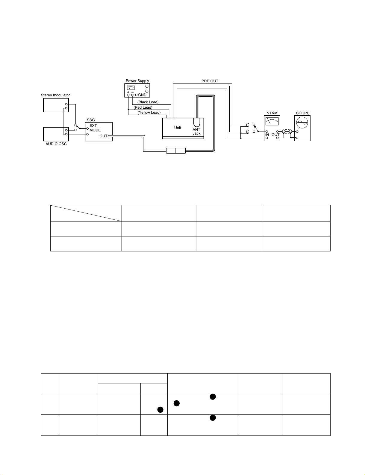
2. FM Adjustment
Figure 3.
(1) The impedance of FM antenna terminal is 75Ω
Therefore, connect coaxial cable (3C-2V etc.) between FM SG and antenna terminal when wiring.
(2) There are two kind in indication of FM SG output attenuator.
1) Attenuator with Marking of 75Ω open...open indication type.
2) Attenuator with marking of 75Ω load or close...load or close indication type.
(3) FM SG output level in this FM adjustment are described as open indication type. The left table shows
relations among FM SG attenuator indication(dB), available power ratio(dBf) and antenna terminal
voltage(dB/µV) in each indication type.
Notes:
1. BAND Switch
........................................................................................................................................
FM
2. BALANCE
.......................................................................................................................................
Center
3. TREBLE/BASS
................................................................................................................................
Center
4. Connect as shown in figure 3.
5. Refer to figure 1~2 for Adjustment Points.
Item FM SSG Attenuator Available Antenna
Type Indication Power Ratio Terminal Voltage
Open indication type
0dB 5.2dBf 6dB/µV
60dB 65.2dBf 66dB/µV
Load or close 0dB 11.2dBf 12dB/µV
indication type 54dB 65.2dBf 66dB/µV
FEED SIGNAL
STEP SUBJECT
FROM TO
MEASURE OUTPUT ADJUSTMENT ADJUST FOR
1 Discriminator 98MHz 60dB ANT Jack Between Point XX & Point T101 DC 0V±10mV
22.5kHz Dev. or XX, DC Volt Meter.
1kHz FM SSG Point XX
2 MPX 98MHz 60dB Same as Between Point XX & GND, VR301 76kHz±50Hz
Adjustment
75kHz Dev.1kHz
above
Frequency Counter
FM SSG
A
C
D
E
Page 8

- 2-3 -
3. AM(MW) Adjustment
Notes:
1. BAND Switch
...................................................................................................................................
AM(MW)
2. Connect as shown in figure 4.
3. Refer to figure 1~2 for Adjustment Points.
Figure 4.
FEED SIGNAL
STEP SUBJECT
FROM TO
MEASURE OUTPUT ADJUSTMENT ADJUST FOR
1 520 or 522kHz No Input LCD Display TUNE +/- Button 520 or 522kHz
(Reception Frequency)
Tuning Voltage Between Point XX and GND, L206 DC 1.2V ± 0.05V
Adjustment DC Volt Meter
2 IF Coil 600kHz or ANT Jack Output L or R ch, T201 & T202 Max. Output
Adjustment 603kHz ANT or PointXX VTVM & Oscilloscope
input, 30dB,
400Hz (30%
MOD) SSG.
3 600kHz or 600kHz or Same as LCD Display TUNE +/- Button 600 or 603kHz
603kHz 603kHz ANT above (Reception Frequency)
RF Adjustment input, 30dB,
400Hz (30%
Output L or R ch, L204 & L205 Max. Output
MOD) SG.
VTVM & Oscilloscope
A
B
Page 9

- 2-4 -
4. LW Adjustment(Optional)
Notes:
1. BAND Switch
...........................................................................................................................................
LW
2. Connect as shown in figure 5.
3. Refer to figure 1~2 for Adjustment Points.
Figure 5.
FEED SIGNAL
STEP SUBJECT
FROM TO
MEASURE OUTPUT ADJUSTMENT ADJUST FOR
1 144kHz No Input LCD Display TUNE +/- Button 144kHz
(Reception Frequency)
Tuning Voltage Between Point XX and GND, L256 DC 1.2V ± 0.05V
Adjustment DC Volt Meter
2 150kHz 150kHz ANT Jack LCD Display TUNE +/- Button 150kHz
RF Adjustment ANT input, or PointXX (Reception Frequency)
30dB, 400Hz
(30% MOD)
Output L or R ch, L254 & L255 Max. Output
SSG.
VTVM & Oscilloscope
A
B
Page 10

- 2-5 -
5. Cassette Deck Adjustment
(1) Before this adjustment, clean PLAYBACK head surface.
(2) For this adjustment, use test tape MTT-114.
(3) VOLUME
......................................
Center
(4) BALANCE
....................................
Center
(5) TREBLE/BASS
............................
Center
(6) Connect as shown in figure 6.
Figure 6.
Figure 7.
SUBJECT MEASURE OUTPUT SETTING ADJUSTMENT ADJUST FOR REMARKS
P.B Head L-CH, R-CH, VTVM and Playback(FWD & Adjust the azimuth Max. Output After this
Adjustment Scope See figure 6. REV) the TEST adjusting screw both channels adjustment, lock
TAPE MTT-114 (in figure 7). on FWD and the screw with
REV PLAY paint.
Forward Head Azimuth
Adjustment Screw
Head
Screw Driver
Reverse Head Azimuth
Adjustment Screw
Page 11

- 2-6 -
INTERNAL BLOCK DIAGRAM of Ics
■ IC101 DBL 1018(LA 1 140)
■ IC201 DBL 1019 (LA1 135)
Page 12

- 2-7 -
■ IC301 KIA6043S
NOTE: Mark terminals are not existence in KIC9256P, KIC9256F
Terminal name of KIC9256P, KIC9256F is shown in parentheses.
Others are common terminals.
■ IC401 KIC9256P
Page 13

- 2-8 -
■ IC402 μμPD789104GS-204
PIN Port P-NAME I/O Act DESCRIPTION When not used REMARK
1 P23 FRTCLK O FRONT IC CLOCK Data OUTPUT
I DIODE MATRIX as DIO IN2 line
2 P24 ACC IN I ACC DETECT INPUT ACTIVE = LOW
3 P25 CDC DI I L CD CHANGER DATA INPUT
4 Avdd A/D Reference Voltage (5V)
5 P60 KEYIN I AD KEY - IN input.
Used for also front panel detecting.
Less than 0.17V : regarded as the panel opened.
Refer to application circuit.
6 P61 DIR I H/L TAPE DIRECTION INPUT (H = FORWARD)
7 P62 SD Tuner SEEK stop detector input
- Seek Stop threshold voltage :
AM : 1.2V, FM : 1.5V
8 P63 STIN I L FM Stereo detect input Active = Low
9 AVSS GROUND
10 NC NO CONNECTION
11 P50 CDCO O CDC Data Output : Should be connected to CDCI
12 P51 PEVDATA O E VR Communication DATA OUT
13 P52 MUTE/LED O Used as Power IC mute. Active = Low
Used as blinking LED. On duty = 10%
14 P53 TPMUTE I L TAPE MUTE INPUT (LOW = MUTE)
15 P00 FRTDO/ O FRONT IC DATA Out communication port
DIO IN0 I Diode matrix IN0 input
16 P01 CDON O H When CDC mode this port is high output
(future function)
17 P02 POWER O H When system is on, this port is used as power out
port
18 P03 TAPE IN I H For tape mode, Active high voltage should be applied.
L = RADIO mode.
19 RESET RESET INPUT
20 IC Connect to GROUND
21 NC NO CONNECTION
22 X2 X-tal
23 X1 X-tal
24 Vss System ground
25 Vdd System Power Supply (5V)
26 P10 FINH O L Front IC INH port.
27 P11 PERI/ O PLL IC PERIODE communication port
DIO OUT2 O Diode matrix DIO OUT 2 line
28 P20 PEVCLK O PLL IC and E. VOL IC CLOCK communication port
DIO OUT0 O Diode matrix DIO OUT 0 line
29 P21 PDATA O PLL IC DATA communication port
DIO OUT1 O Diode matrix DIO OUT 1 line
30 P22 FRTCE O FRONT IC CE communication port
DIO IN1 I Diode matrix DIO IN 1 line
Page 14

- 2-9 -
■ IC501 LA3160
■ IC601 PT2313L
Page 15

- 2-10 -
■ IC801 TDA8571J
■ IC901 LC75833E
Page 16

- 2-11 -
BLOCK DIAGRAM
NOTE: Block diagram for this model are subject to change for improvement without prior notice.
Page 17

- 2-12 -
WIRING DIAGRAM(Deck Mechanism)
CN502
ICC • 100H
CN501
IEE • 100H
BANDING
OWR1305R091
OWR1306R091
LEAF SW
HEAD SW PWG
BANDING
BH BL
RDWHBK
RO
MOTOR
DECK P/N : 6730R-K001A
RO
BK
HOLDER P/N : 324-973B
WH
Page 18

2-13 2-14
SCHEMATIC DIAGRAM (TCC-6210)
R
L
NOTE: 1. Resistance values are indicated in ohms unless otherwise specified (K=1,000, M=1,000,000).
2. Capacitance values are shown in microfarads unless otherwise (P=MICRO-MICRO FARADS).
3. Schematic diagram for this model are subject to change for improvement without prior notice.
Page 19

2-16 2-15
PCB LAYOUT
• MAIN P.C. BOARD(SOLDER SIDE)
Page 20

2-17 2-18
• MAIN P.C. BOARD(COMPONENT SIDE)
Page 21

2-20 2-19
• FRONT P.C. BOARD MODEL: TCC-6210
NEW RF P.C. BOARD
(TOP VIEW)
(BOTTOM VIEW)
Page 22

3-1 3-2
SECTION 3. CABINET MAIN CHASSIS & MECHANISM
EXPLODED VIEW & PART LIST
• Main Section
302
A42
A43
271
273
276
275
A47
280
274
272
276
455
455
455
330
260
320
A55
457
OPTION(353-025F)
301
456
A00
A46
281
288
456
DECK MECHANISM(A00)
SVC Supply unit: Assembly only!
CAUTION
Exposed blade will cause
severe injury
NOTE) Refer to “SECTION 4 REPLACEMENT
PARTS LIST” in order to look for the
part number of each part.
 Loading...