

COLOR MONITOR
SERVICE MANUAL
Website:http://biz.LGservice.com
E-mail:http://www.LGEservice.com/techsup.html
CAUTION
BEFORE SERVICING THE UNIT,
READ THE SAFETY PRECAUTIONS IN THIS MANUAL.
MODEL:
T730SH
(T730SHMKQ-K***V*)
CHASSIS NO. : CM54A
( ) **Same model for Service
*Same looking with new chassis.
CONTENTS
SPECIFICATIONS ................................................... 2
SAFETY PRECAUTIONS ........................................
SERVICE PRECAUTION.......................................... 4
TIMING CHART ....................................................... 7
WIRING DIAGRAM ................................................. 9
DISASSEMBLY ....................................................... 8
BLOCK DIAGRAM ...................................................
10
SPECIFICATIONS
1. PICTURE TUBE
Size : 17 inch
DefIection Angle : 90¡
Neck Diameter : 29.1 mm
Stripe Pitch : 0.25 mm
Face Treatment : W-ARASC (Anti-Reflection and
Anti-Static Coating)
Internal : Anti-Glare
2. SIGNAL
2-1. Horizontal & Vertical Sync
1) Input Voltage Level : Low=0~1.2V, High=2.5~5.5V
2) Sync Polarity : Positive or Negative
2-2. Video Input Signal
1) Voltage Level : 0 ~ 0.7 Vp-p
a) Color 0, 0 : 0 Vp-p
b) Color 7, 0 : 0.467 Vp-p
c) Color 15, 0 : 0.7 Vp-p
2) Input Impedance : 75
3) Video Color : R, G, B Analog
4) Signal Format : Refer to the Timing Chart
2-3. Signal Connector
3 row 15-pin Connector (Attached)
2-4. Scanning Frequency
Horizontal : 30 ~ 71 kHz
Vertical : 50 ~ 160 Hz
3. POWER SUPPLY
3-1. Power Range
AC 100-240V~ 50/ 60Hz, 1.0A
DESCRIPTION OF BLOCK DIAGRAM................... 11
3
ADJUSTMENT ....................................................... 13
TROUBLESHOOTING GUIDE .............................. 19
EXPLODED VIEW...................................................35
SCHEMATIC DIAGRAM ......................................... 37
PRINTED CIRCUIT BOARD................................... 39
3-2. Power Consumption
MODE
NORMAL (ON)
DPMS OFF
POWER OFF
VIDEO
YES
NO
NO
4. DISPLAY AREA
4-1. Active Video Area :
Max Image Size - 325.1 x 243.8 mm (12.80" x 9.60")
Preset Image Size - 310 x 230 mm (12.20" x 9.06")
4-2. Display Color : Full Colors
4-3. Display Resolution : 1280 x 1024 / 60Hz(Max)
4-4. Video Bandwidth : 110 MHz
5. ENVIRONMENT
5-1. Operating Temperature: 0¡C ~ 40¡C
5-2. Relative Humidity : 10%~ 80%
5-3. Altitude : 5,000 m
6. DIMENSIONS (with TILT/SWIVEL)
Width : 400 mm (15.75 inch)
Depth : 411 mm (16.18 inch)
Height : 401 mm (15.79 inch)
7. WEIGHT (with TILT/SWIVEL)
Net Weight : 13.3 kg
Gross Weight : 16.2 kg
POWER CONSUMPTION
less than 63 W
less than 3 W
less than 3 W
(Non-Interlace)
(Ambient)
(Non-condensing)
LED COLOR
BLUE
FLICKER
OFF
- 2 -
SAFETY PRECAUTIONS
- 3 -
SAFETY-RELATED COMPONENT WARNING!
There are special components used in this color monitor
which are important for safety. These parts are marked
on the schematic diagram and the replacement
parts list. It is essential that these critical parts should be
replaced with the manufacturer's specified parts to prevent
X-radiation, shock, fire, or other hazards. Do not modify
the original design without obtaining written permission
from manufacturer or you will void the original parts and
labor guarantee.
CAUTION:
No modification of any circuit should be
attempted.
Service work should be performed only after
you are thoroughly familiar with all of the
following safety checks and servicing
guidelines.
SAFETY CHECK
Care should be taken while servicing this color monitor
because of the high voltage used in the deflection circuits.
These voltages are exposed in such areas as the
associated flyback and yoke circuits.
FIRE & SHOCK HAZARD
An isolation transformer must be inserted between the
color monitor and AC power line before servicing the
chassis.
• In servicing, attention must be paid to the original lead
dress specially in the high voltage circuit. If a short
circuit is found, replace all parts which have been
overheated as a result of the short circuit.
• All the protective devices must be reinstalled per the
original design.
• Soldering must be inspected for the cold solder joints,
frayed leads, damaged insulation, solder splashes, or
the sharp points. Be sure to remove all foreign
materials.
IMPLOSION PROTECTION
All used display tubes are equipped with an integral
implosion protection system, but care should be taken to
avoid damage and scratching during installation. Use only
same type display tubes.
X-RADIATION
The only potential source of X-radiation is the picture tube.
However, when the high voltage circuitry is operating
properly there is no possibility of an X-radiation problem.
The basic precaution which must be exercised is keep the
high voltage at the factory recommended level; the normal
high voltage is about 25.8kV. The following steps describe
how to measure the high voltage and how to prevent Xradiation.
Note : It is important to use an accurate high voltage
meter calibrated periodically.
• To measure the high voltage, use a high impedance
high voltage meter, connect (–) to chassis and (+) to
the CDT anode cap.
• Set the brightness control to maximum point at full
white pattern.
• Measure the high voltage. The high voltage meter
should be indicated at the factory recommended level.
• If the meter indication exceeds the maximum level,
immediate service is required to prevent the possibility
of premature component failure.
• To prevent X-radiation possibility, it is essential to use
the specified picture tube.
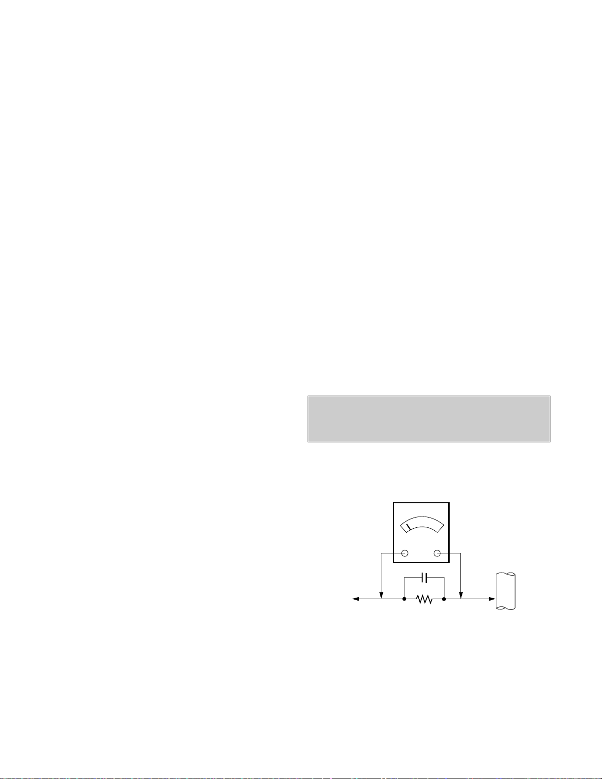
Leakage Current Hot Check Circuit
CAUTION:
Please use only a plastic screwdriver to protect yourself
from shock hazard during service operation.
1.5 Kohm/10W
To Instrument's
exposed
METALLIC PARTS
Good Earth Ground
such as WATER PIPE,
CONDUIT etc.
AC Volt-meter

- 4 -
SERVICING PRECAUTIONS
CAUTION: Before servicing receivers covered by this
service manual and its supplements and addenda, read
and follow the SAFETY PRECAUTIONS on page 3 of this
publication.
NOTE: If unforeseen circumstances create conflict
between the following servicing precautions and any of the
safety precautions on page 3 of this publication, always
follow the safety precautions. Remember: Safety First.
General Servicing Precautions
1. Always unplug the receiver AC power cord from the AC
power source before;
a. Removing or reinstalling any component, circuit
board module or any other receiver assembly.
b. Disconnecting or reconnecting any receiver electrical
plug or other electrical connection.
c. Connecting a test substitute in parallel with an
electrolytic capacitor in the receiver.
CAUTION: A wrong part substitution or incorrect
polarity installation of electrolytic capacitors may
result in an explosion hazard.
d. Discharging the picture tube anode.
2. Test high voltage only by measuring it with an
appropriate high voltage meter or other voltage
measuring device (DVM, FETVOM, etc) equipped with
a suitable high voltage probe.
Do not test high voltage by "drawing an arc".
3. Discharge the picture tube anode only by (a) first
connecting one end of an insulated clip lead to the
degaussing or kine aquadag grounding system shield
at the point where the picture tube socket ground lead
is connected, and then (b) touch the other end of the
insulated clip lead to the picture tube anode button,
using an insulating handle to avoid personal contact
with high voltage.
4. Do not spray chemicals on or near this receiver or any
of its assemblies.
5. Unless specified otherwise in this service manual,
clean electrical contacts only by applying the following
mixture to the contacts with a pipe cleaner, cottontipped stick or comparable non-abrasive applicator;
10% (by volume) Acetone and 90% (by volume)
isopropyl alcohol (90%-99% strength)
CAUTION: This is a flammable mixture.
Unless specified otherwise in this service manual,
lubrication of contacts in not required.
6. Do not defeat any plug/socket B+ voltage interlocks
with which receivers covered by this service manual
might be equipped.
7. Do not apply AC power to this instrument and/or any of
its electrical assemblies unless all solid-state device
heat sinks are correctly installed.
8. Always connect the test receiver ground lead to the
receiver chassis ground before connecting the test
receiver positive lead.
Always remove the test receiver ground lead last.
9. Use with this receiver only the test fixtures specified in
this service manual.
CAUTION: Do not connect the test fixture ground strap
to any heat sink in this receiver.
Electrostatically Sensitive (ES) Devices
Some semiconductor (solid-state) devices can be
damaged easily by static electricity. Such components
commonly are called Electrostatically Sensitive (ES)
Devices. Examples of typical ES devices are integrated
circuits and some field-effect transistors and
semiconductor "chip" components. The following
techniques should be used to help reduce the incidence of
component damage caused by static by static electricity.
1. Immediately before handling any semiconductor
component or semiconductor-equipped assembly, drain
off any electrostatic charge on your body by touching a
known earth ground. Alternatively, obtain and wear a
commercially available discharging wrist strap device,
which should be removed to prevent potential shock
reasons prior to applying power to the unit under test.
2. After removing an electrical assembly equipped with
ES devices, place the assembly on a conductive
surface such as aluminum foil, to prevent electrostatic
charge buildup or exposure of the assembly.
3. Use only a grounded-tip soldering iron to solder or
unsolder ES devices.
4. Use only an anti-static type solder removal device.
Some solder removal devices not classified as "antistatic" can generate electrical charges sufficient to
damage ES devices.
5. Do not use freon-propelled chemicals. These can
generate electrical charges sufficient to damage ES
devices.
6. Do not remove a replacement ES device from its
protective package until immediately before you are
ready to install it. (Most replacement ES devices are
packaged with leads electrically shorted together by
conductive foam, aluminum foil or comparable
conductive material).
7. Immediately before removing the protective material
from the leads of a replacement ES device, touch the
protective material to the chassis or circuit assembly
into which the device will be installed.
CAUTION: Be sure no power is applied to the chassis
or circuit, and observe all other safety precautions.
8. Minimize bodily motions when handling unpackaged
replacement ES devices. (Otherwise harmless motion
such as the brushing together of your clothes fabric or
the lifting of your foot from a carpeted floor can
generate static electricity sufficient to damage an ES
device.)

- 5 -
General Soldering Guidelines
1. Use a grounded-tip, low-wattage soldering iron and
appropriate tip size and shape that will maintain tip
temperature within the range or 500
F to 600 F.
2. Use an appropriate gauge of RMA resin-core solder
composed of 60 parts tin/40 parts lead.
3. Keep the soldering iron tip clean and well tinned.
4. Thoroughly clean the surfaces to be soldered. Use a
mall wire-bristle (0.5 inch, or 1.25cm) brush with a
metal handle.
Do not use freon-propelled spray-on cleaners.
5. Use the following unsoldering technique
a. Allow the soldering iron tip to reach normal
temperature.
(500
F to 600 F)
b. Heat the component lead until the solder melts.
c. Quickly draw the melted solder with an anti-static,
suction-type solder removal device or with solder
braid.
CAUTION: Work quickly to avoid overheating the
circuitboard printed foil.
6. Use the following soldering technique.
a. Allow the soldering iron tip to reach a normal
temperature (500
F to 600 F)
b. First, hold the soldering iron tip and solder the strand
against the component lead until the solder melts.
c. Quickly move the soldering iron tip to the junction of
the component lead and the printed circuit foil, and
hold it there only until the solder flows onto and
around both the component lead and the foil.
CAUTION: Work quickly to avoid overheating the
circuit board printed foil.
d. Closely inspect the solder area and remove any
excess or splashed solder with a small wire-bristle
brush.
IC Remove/Replacement
Some chassis circuit boards have slotted holes (oblong)
through which the IC leads are inserted and then bent flat
against the circuit foil. When holes are the slotted type,
the following technique should be used to remove and
replace the IC. When working with boards using the
familiar round hole, use the standard technique as
outlined in paragraphs 5 and 6 above.
Removal
1. Desolder and straighten each IC lead in one operation
by gently prying up on the lead with the soldering iron
tip as the solder melts.
2. Draw away the melted solder with an anti-static
suction-type solder removal device (or with solder
braid) before removing the IC.
Replacement
1. Carefully insert the replacement IC in the circuit board.
2. Carefully bend each IC lead against the circuit foil pad
and solder it.
3. Clean the soldered areas with a small wire-bristle
brush. (It is not necessary to reapply acrylic coating to
the areas).
"Small-Signal" Discrete Transistor
Removal/Replacement
1. Remove the defective transistor by clipping its leads as
close as possible to the component body.
2. Bend into a "U" shape the end of each of three leads
remaining on the circuit board.
3. Bend into a "U" shape the replacement transistor leads.
4. Connect the replacement transistor leads to the
corresponding leads extending from the circuit board
and crimp the "U" with long nose pliers to insure metal
to metal contact then solder each connection.
Power Output, Transistor Device
Removal/Replacement
1. Heat and remove all solder from around the transistor
leads.
2. Remove the heat sink mounting screw (if so equipped).
3. Carefully remove the transistor from the heat sink of the
circuit board.
4. Insert new transistor in the circuit board.
5. Solder each transistor lead, and clip off excess lead.
6. Replace heat sink.
Diode Removal/Replacement
1. Remove defective diode by clipping its leads as close
as possible to diode body.
2. Bend the two remaining leads perpendicular y to the
circuit board.
3. Observing diode polarity, wrap each lead of the new
diode around the corresponding lead on the circuit
board.
4. Securely crimp each connection and solder it.
5. Inspect (on the circuit board copper side) the solder
joints of the two "original" leads. If they are not shiny,
reheat them and if necessary, apply additional solder.
Fuse and Conventional Resistor
Removal/Replacement
1. Clip each fuse or resistor lead at top of the circuit board
hollow stake.
2. Securely crimp the leads of replacement component
around notch at stake top.
3. Solder the connections.
CAUTION: Maintain original spacing between the
replaced component and adjacent components and the
circuit board to prevent excessive component
temperatures.

- 6 -
Circuit Board Foil Repair
Excessive heat applied to the copper foil of any printed
circuit board will weaken the adhesive that bonds the foil
to the circuit board causing the foil to separate from or
"lift-off" the board. The following guidelines and
procedures should be followed whenever this condition is
encountered.
At IC Connections
To repair a defective copper pattern at IC connections use
the following procedure to install a jumper wire on the
copper pattern side of the circuit board. (Use this
technique only on IC connections).
1. Carefully remove the damaged copper pattern with a
sharp knife. (Remove only as much copper as
absolutely necessary).
2. carefully scratch away the solder resist and acrylic
coating (if used) from the end of the remaining copper
pattern.
3. Bend a small "U" in one end of a small gauge jumper
wire and carefully crimp it around the IC pin. Solder the
IC connection.
4. Route the jumper wire along the path of the out-away
copper pattern and let it overlap the previously scraped
end of the good copper pattern. Solder the overlapped
area and clip off any excess jumper wire.
At Other Connections
Use the following technique to repair the defective copper
pattern at connections other than IC Pins. This technique
involves the installation of a jumper wire on the
component side of the circuit board.
1. Remove the defective copper pattern with a sharp
knife.
Remove at least 1/4 inch of copper, to ensure that a
hazardous condition will not exist if the jumper wire
opens.
2. Trace along the copper pattern from both sides of the
pattern break and locate the nearest component that is
directly connected to the affected copper pattern.
3. Connect insulated 20-gauge jumper wire from the lead
of the nearest component on one side of the pattern
break to the lead of the nearest component on the
other side.
Carefully crimp and solder the connections.
CAUTION: Be sure the insulated jumper wire is
dressed so the it does not touch components or sharp
edges.
- 7 -
TIMING CHART
* No Composite Mode.
<< Dot Clock (MHz), Horizontal Frequency (kHz), Vertical Frequency (Hz), Horizontal etc... (µs), Vertical etc... (ms) >>
A
B
C
D
E
F
Video
Sync
MODE
1 2 3 4
Polarity
- + + +
H H-Frequency KHz
37.500 46.880 53.680 68.677
O H-Active (A) uS
26.670 21.330 18.630 14.561
R H-Video(B) uS
20.320 16.160 14.220 10.836
I H-blanking(C) uS
6.350 5.170 4.410 3.725
Z H-front porch(D) uS
0.510 0.320 0.570 0.508
H-sync time(E) uS
2.030 1.620 1.140 1.016
H-back porch(F) us
3.810 3.223 2.700 2.201
Polarity
- + + +
V-Frequency Hz
74.990 75.010 85.070 85.000
V-Active (A) mS
13.335 13.331 11.755 11.764
V V -Video(B) mS
12.802 12.798 11.178 11.182
E V-blanking(C) mS
0.533 0.533 0.577 0.582
R V-front porch(D) mS
0.026 0.021 0.018 0.014
T V-sync time(E) mS
0.080 0.064 0.056 0.044
V-back porch(F) mS
0.427 0.448 0.503 0.524
Resolution
640* 800* 800* 1024*
480 600 600 768
VESA
- 8 -
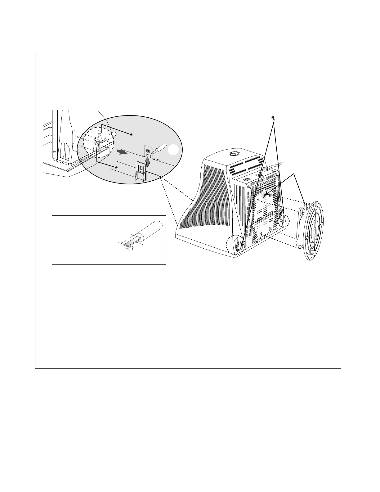
DIS A S S E MB LY
1. T IL T /S WIV E L & B A C K C OV ER R E MOV AL
1) S et the monitor fac e downward.
2) C arefully remove the T ilt/S wivel by pulling it upward.
3) Remove the screw (b), Back cover by pushing it upward.
4) R eleas e the latch (c). (S ee T ip S pec.)
5) S lide the B ack C over a wa y from the F ront C abinet of the monitor.
Tip S pec .
A(W idth) : 5.0~15. 0mm
B (Depth) : 0.6~0.9mm
C (Height) : 12.0mm
B a
ck
C ov e
r
(c )
C abin et
(b)
(a )
C
T ip
B
A
WIRING DIAGRAM
- 9 -
P501
P201
P405
P301
P302
G2
P702
P701
T1
P402
P902
S
+
S
Signal
Cable
AC
Socket
FBT
P220
P203
P202
P904
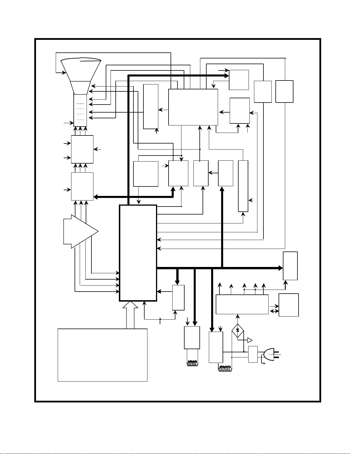
BLOCK DIAGRAM
- 1 0 -
Dynamic Focus
Static Focus
H.V
DY CDT
Screen
Heater ( 6.3V )
VIDEO
8V 80V
G1
G2
as
i
B
G/B
(IC303)
Main AM P
R/
15V
- 160V
Brightness Control
FBT
( T701 )
40V
15V
Auto
Beam
LimitDC/DC Converter
D/D
Feed Back
Circuit
FOCUS
Dynamic
B+
5V
Circuit
Regulation
X-R AY
Circuit
Protection
OSD
VIDEO
5V
Video
H-Sync
Pre- AMP /
RGB
Signal
V-Sync
(IC302)
SCL / SDA
H-Sync/V-Sync
PWM Control Signal
( IC 401 )
C CLOCK(SCL)
2
I
C DATA(SD A)
2
I
SAA4849
MICOM & H/V Sync Processor
V-Out
( IC 601)
15V
C
2
I
PROM
2
E
(IC402)
5V
6.3V
H-Out
TDA4867J
( Q706)
15V
H-Linearity
Correction
50V
H - Drive
B-Drive
DPM
Control
Circuit
15V
50V
80V
SMPS
(T901)
V
15
5V
6.3V
Voltage
feedback
SMPS
Control
(IC901)
BRIGHTNESS
TILT
Control
Circuit
Circuit
MOIRE
CONTRAST
SPCC
H / V SI ZE
TRAPEZOID
DEG AUSSING
H / V POSI TION
PIN BAL ANC E
COLOR
OSD TIME
LANGU AGE
VIDEO LEVEL
INFORMATION
ROTATION (Tilt)
RECALL / RESET
PAR ALL ELOGR AM
TOP/BOTTOM CORNER
OSD CONTROL LOCK
[ OSD Control ]
TILT
Coil
Degaussing
Line
Filter
(50/60Hz)
Power Input
100~240V AC
Degaussing
Coil

DESCRIPTION OF BLOCK DIAGRAM
- 11 -
1. SMPS(Switching Mode Power Supply)
When you turn on the power switch, the operating
fprocedure is as follows:
.
6. X-RAY Protection Circuit
When the high Voltage reaches to 29kV in an abnormal case,
the high voltage detector circuit, R818,D721,C739-1 R416,
C409 start operation to shut down high voltage circuit.
7. Horizontal S-correction Circuit.
This circuit corrects the horizontal linearity for each horizontal
sync frequency.
8. Horizontal drive and Output Circuit.
This circuit is a horizontal deflection amplifier for raster scan.
9. ABL Circuit
This circuit limits the beam-current for the reliability of CDT
10. Vertical Output Circuit
This circuit takes the vertical ramp wave from the TDA4867J
(IC601) and perform the vertical deflection by supplying the
saw-tooth wave current to the vertical deflection yoke.
11. Blanking and Brightness Control Circuit.
Blanking circuit eliminates the retrace line by supplying
a negative pulse wave to the G1 of the CDT.
Brightness control circuit is used for control of the screen
brightness by changing the DC level G1.
12. Image Rotation (Tilt) Circuit.
This circuit corrects the tilt of the screen by supplying
the image rotation signal to the tilt coil which is
attached near the deflection yoke of the CDT.
13. OSD (On Screen Display) Circuit.
This circuit displays information of the monitor`s status
on the screen.
14. Video Processor Circuit.
Video processor circuit consists of the video drive output
block. The video drive IC(IC302) receives the video
signal from PC. The gain of each channel is controlled
by MICOM through IIC.
The cut-off circuit compensate different voltage of each
channel between the cathode and the G1 of the CDT.
1) The AC line voltage is rectified by the bridge diode
D900.
2) The control IC(IC901) starts switching and generates
switch pulse in the primary turn of the SMPS
transformer(T901)
3) The switching pulses of the primary turns are induced
to the secondary turns of the transformer by the turn
ratio. This pulses are rectified by each diode(D971,
D961(D962),D951,D942,D941)
4) Each rectified DC voltage(80V, 50V, 15V,6.3V and 5V)
2. Over Voltage Protection Circuit
When the input of IC901 Vin (pin 4) is more than 22V, all the
secondary voltages of the SMPS transformer (T901) down
to low value
3. Display Power Management Circuit(DPM)
1) DPM OFF
When no input of horizontal or vertical sync Q951,
Q941 are turned off .Then input power consumption
is below 4 watts.
4. Microprocessor Control & Horizontal and Vertical Sync
Processor Circuit
The operating procedure is as follows ;
1) There is Horizontal & Vertical process function in
Microprocessor.(IC401)
2) Microprocessor (IC401) discriminates the operating mode
from the sync polarity and resolution.
3) After microprocessor reads these adjusted mode data
stored at EEPROM, it controls operating mode data through
IIC
4) Users can control screen condition by the OSD Select,Up,
Down, Left, Right, Exit.
5. D/D Converter Circuit.
To obtain constant high voltage, this circuit supplies
controlled DC voltage for FBT and horizontal deflection
circuit according to the horizontal sync frequency.

- 12 -
15. Video Pre-Amp Circuit.
This circuit amplifies the analog video signal from 0~0.7 V
to 0~4 V. It is operated by taking the clamp, R,G,B drive
and contrast signal from the MICOM (IC401)
16. Video Output Amp Circuit.
This circuit amplifies the video signal which comes from the
video pre-amp circuit and amplified it to applied the CDT
cathode
 Loading...