

Page 1

MODEL: HT356SD (HT356SD, SH36SD-S/W)SERVICE MANUAL
Internal Use Only
Website http://biz.lgservice.com
DVD HOME THEATER SYSTEM
SERVICE MANUAL
P/NO : AFN75272758 JANUARY, 2011
MODEL: HT356SD
(HT356SD, SH36SD-S/W)
CAUTION
BEFORE SERVICING THE UNIT, READ THE “SAFETY PRECAUTIONS”
IN THIS MANUAL.
Page 2
[CONTENTS]
P SECTION 1. GENERAL
• SERVICING PRECAUTIONS . . . . . . . . . . . . . . . . . . . . . . . . . . . . . . . . . . . . . . . . . . . . . . . . . 1-2
• ESD PRECAUTIONS . . . . . . . . . . . . . . . . . . . . . . . . . . . . . . . . . . . . . . . . . . . . . . . . . . . . . . . 1-4
• SERVICE INFORMATION FOR EEPROM . . . . . . . . . . . . . . . . . . . . . . . . . . . . . . . . . . . . . . 1-5
•
HOW TO UPDATE DVD & AUDIO MICOM PROGRAMS. .
• SPECIFICATIONS . . . . . . . . . . . . . . . . . . . . . . . . . . . . . . . . . . . . . . . . . . . . . . . . . . . . . . . . . 1-7
. . . . . . . . . . . . . . . . . . . . . . . . 1-6
P SECTION 2. ELECTRICAL PART
• TROUBLESHOOTING GUIDE . . . . . . . . . . . . . . . . . . . . . . . . . . . . . . . . . . . . . . . . . . . . . . . . 2-1
• DETAILS AND WAVEFORMS ON SYSTEM TEST AND DEBUGGING . . . . . . . . . . . . . . . 2-13
• WIRING DIAGRAM . . . . . . . . . . . . . . . . . . . . . . . . . . . . . . . . . . . . . . . . . . . . . . . . . . . . . . . 2-27
• OVERALL BLOCK DIAGRAM . . . . . . . . . . . . . . . . . . . . . . . . . . . . . . . . . . . . . . . . . . . . . . . 2-29
• CIRCUIT DIAGRAMS . . . . . . . . . . . . . . . . . . . . . . . . . . . . . . . . . . . . . . . . . . . . . . . . . . . . . . 2-31
• CIRCUIT VOLTAGE CHART . . . . . . . . . . . . . . . . . . . . . . . . . . . . . . . . . . . . . . . . . . . . . . . . 2-41
• PRINTED CIRCUIT DIARGAMS . . . . . . . . . . . . . . . . . . . . . . . . . . . . . . . . . . . . . . . . . . . . . 2-45
P SECTION 3. EXPLODED VIEWS
• CABINET AND MAIN FRAME SECTION . . . . . . . . . . . . . . . . . . . . . . . . . . . . . . . . . . . . . . . . 3-1
• DECK MECHANISM EXPLODED VIEW (DP-15T) . . . . . . . . . . . . . . . . . . . . . . . . . . . . . . . . 3-3
• PACKING ACCESSORY SECTION . . . . . . . . . . . . . . . . . . . . . . . . . . . . . . . . . . . . . . . . . . . . 3-5
• SPEAKER SECTION . . . . . . . . . . . . . . . . . . . . . . . . . . . . . . . . . . . . . . . . . . . . . . . . . . . . . . . 3-6
P SECTION 4. MECHANISM (DP-15T) . . . . . . . . . . . . . . . . . . . . . . . . . . . . . . . . . . . . . . . . 4-1
P SECTION 5. REPLACEMENT PARTS LIST . . . . . . . . . . . . . . . . . . . . . . . . . . . . . . . . . 5-1
1-1
Page 3
SECTION 1. GENERAL
SERVICING PRECAUTIONS
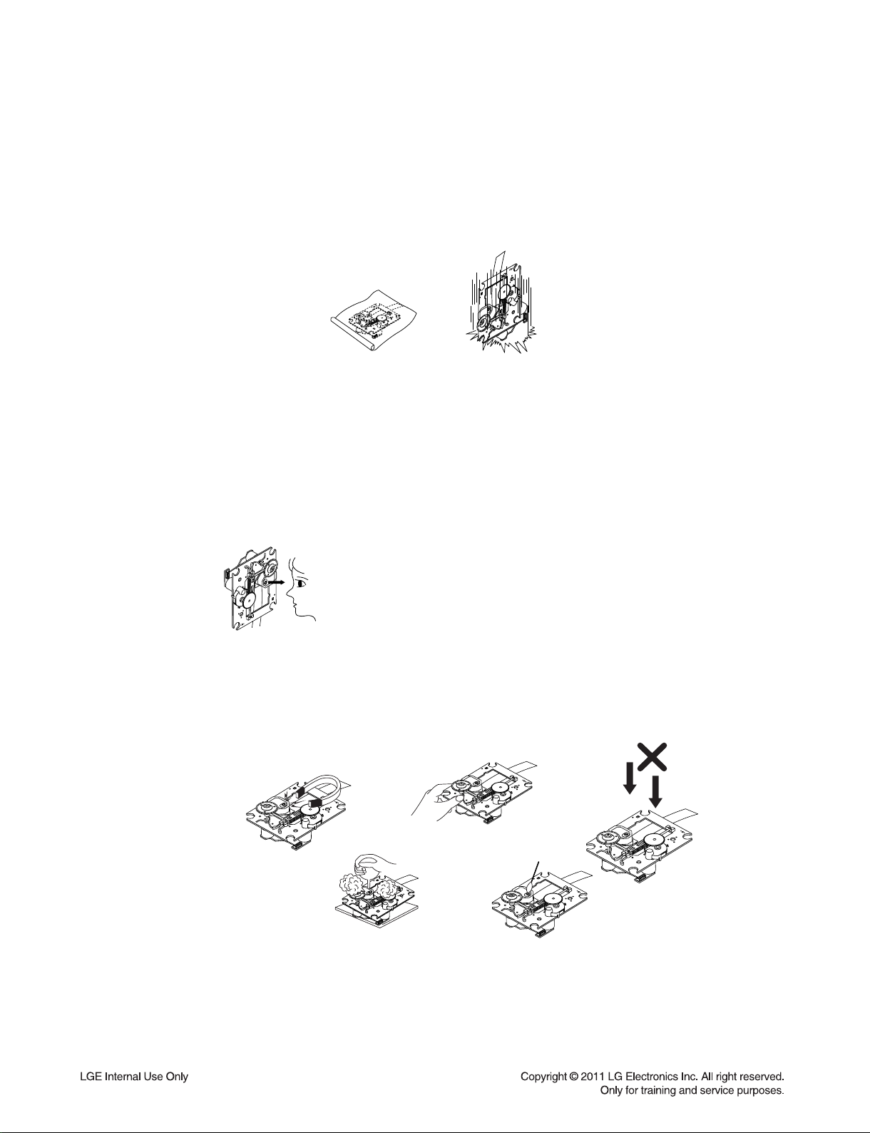
NOTES REGARDING HANDLING OF THE PICK-UP
1. Notes for transport and storage
1) The pick-up should always be left in its conductive bag until immediately prior to use.
2) The pick-up should never be subjected to external pressure or impact.
Storage in conductive bag
2. Repair notes
1) The pick-up incorporates a strong magnet, and so should never be brought close to magnetic materials.
2) The pick-up should always be handled correctly and carefully, taking care to avoid external pressure and
impact. If it is subjected to strong pressure or impact, the result may be an operational malfunction and/or
damage to the printed-circuit board.
3) Each and every pick-up is already individually adjusted to a high degree of precision, and for that reason
the adjustment point and installation screws should absolutely never be touched.
4) Laser beams may damage the eyes!
Absolutely never permit laser beams to enter the eyes!
Also NEVER switch ON the power to the laser output part (lens, etc.) of the pick-up if it is damaged.
NEVER look directly at the laser beam, and don’t allow
contact with fingers or other exposed skin.
5) Cleaning the lens surface
If there is dust on the lens surface, the dust should be cleaned away by using an air bush (such as used
for camera lens). The lens is held by a delicate spring. When cleaning the lens surface, therefore, a cotton swab should be used, taking care not to distort lens.
Drop impact
Pressure
Magnet
How to hold the pick-up
Cotton swab
Conductive Sheet
6) Never attempt to disassemble the pick-up.
Spring has excess pressure. If the lens is extremely dirty, apply isopropyl alcohol to the cotton swab.
(Do not use any other liquid cleaners, because they will damage the lens.) Take care not to use too much
of this alcohol on the swab, and do not allow the alcohol to get inside the pick-up.
1-2
Pressure
Page 4
NOTES REGARDING COMPACT DISC PLAYER REPAIRS
1. Preparations
1) Compact disc players incorporate a great many ICs as well as the pick-up (laser diode). These components
are sensitive to, and easily affected by, static electricity. If such static electricity is high voltage, components
can be damaged, and for that reason components should be handled with care.
2) The pick-up is composed of many optical components and other high-precision components. Care must be
taken, therefore, to avoid repair or storage where the temperature or humidity is high, where strong magnetism is present, or where there is excessive dust.
2. Notes for repair
1) Before replacing a component part, first disconnect the power supply lead wire from the unit
2) All equipment, measuring instruments and tools must be grounded.
3) The workbench should be covered with a conductive sheet and grounded.
When removing the laser pick-up from its conductive bag, do not place the pick-up on the bag. (This is
because there is the possibility of damage by static electricity.)
4) To prevent AC leakage, the metal part of the soldering iron should be grounded.
5) Workers should be grounded by an armband (1M Ω)
6) Care should be taken not to permit the laser pick-up to come in contact with clothing, in order to prevent
static electricity changes in the clothing to escape from the armband.
7) The laser beam from the pick-up should NEVER be directly facing the eyes or bare skin.
Armband
Resistor
(1 Mohm)
Resistor
(1 Mohm)
Conductive
Sheet
1-3
Page 5
ESD PRECAUTIONS
Electrostatically Sensitive Devices (ESD)
Some semiconductor (solid state) devices can be damaged easily by static electricity. Such components
commonly are called Electrostatically Sensitive Devices (ESD). Examples of typical ESD devices are integrated
circuits and some field-effect transistors and semiconductor chip components. The following techniques should
be used to help reduce the incidence of component damage caused by static electricity.
1. Immediately before handling any semiconductor component or semiconductor-equipped assembly, drain off
any electrostatic charge on your body by touching a known earth ground. Alternatively, obtain and wear a
commercially available discharging wrist strap device, which should be removed for potential shock reasons
prior to applying power to the unit under test.
2. After removing an electrical assembly equipped with ESD devices, place the assembly on a conductive surface
such as aluminum foil, to prevent electrostatic charge buildup or exposure of the assembly.
3. Use only a grounded-tip soldering iron to solder or unsolder ESD devices.
4. Use only an anti-static solder removal device. Some solder removal devices not classified as "anti-static" can
generate electrical charges sufficient to damage ESD devices.
5. Do not use freon-propelled chemicals. These can generate electrical charges sufficient to damage ESD
devices.
6. Do not remove a replacement ESD device from its protective package until immediately before you are
ready to install it. (Most replacement ESD devices are packaged with leads electrically shorted together by
conductive foam, aluminum foil or comparable conductive materials).
7. Immediately before removing the protective material from the leads of a replacement ESD device, touch the
protective material to the chassis or circuit assembly into which the device will by installed.
CAUTION : BE SURE NO POWER IS APPLIED TO THE CHASSIS OR CIRCUIT, AND OBSERVE ALL OTHER
SAFETY PRECAUTIONS.
8. Minimize bodily motions when handing unpackaged replacement ESD devices. (Otherwise harmless motion
such as the brushing together of your clothes fabric or the lifting of your foot from a carpeted floor can generate
static electricity sufficient to damage an ESD device).
CAUTION. GRAPHIC SYMBOLS
THE LIGHTNING FLASH WITH APROWHEAD SYMBOL. WITHIN AN EQUILATERAL TRIANGLE, IS
INTENDED TO ALERT THE SERVICE PERSONNEL TO THE PRESENCE OF UNINSULATED
“DANGEROUS VOLTAGE” THAT MAY BE OF SUFFICIENT MAGNITUDE TO CONSTITUTE A RISK OF
ELECTRIC SHOCK.
THE EXCLAMATION POINT WITHIN AN EQUILATERAL TRIANGLE IS INTENDED TO ALERT THE
SERVICE PERSONNEL TO THE PRESENCE OF IMPORTANT SAFETY INFORMATION IN SERVICE
LITERATURE.
1-4
Page 6
SERVICE INFORMATION FOR EEPROM
HEX
<C>
F1
00
A4
AD
00
09
A0
26
50
08
NAME
OPT 1
OPT 2
OPT 3
OPT 4
OPT 5
OPT 6
OPT 7
OPT 8
OPT 9
OPT A
HEX
F1
00
A4
DD
00
09
A0
26
50
08
HEX
<A> <B>
F1
00
A4
DD
00
09
A0
22
50
08
Applicable Models*
<A> HT356SD-A2.BKENHLK
<B> HT356SD-A2.BMARLLK
<C> HT356SD-A2.BZAFLLK
POWER ON
DVD LOGO Status (NO Disk status)
Remote control
Pause key-->1-->4-->7-->2 in order.
Press number 0~9, Press character
A~F (1~6 for a while)
V
V
Use arrow key (
V
V
) to move
to appropriate position and make
changes
Press pause key once
DETECT NEW EEPROM
(OPTION EDIT SCREEN)
Change will be applied when power
OFF-->ON.
1-5
Page 7

HOW TO UPDATE DVD & AUDIO MICOM PROGRAMS
1. The Whole Sequence
1) DVD program download.
2) Power cord out −> in.
3) Audio micom program download.
4) Remote control Pause key ‘\\’ + ‘1472’ for input options.
5) Enter into the system information for check the version, options and check sum.
6) Power off −> on.
Attention:
After DVD program download, never input options and check the version before power cord out.
2. How to enter into System Information
1) Enter into SETUP menu in NO Disc.
2) Put on cursor [Highlight] 16:9 wide option of TV aspect in SETUP menu.
3) Press follow key in continuous using remote control.
1 −> 3 −> 9 −> 7 −> 1 −> 3 −> 9 −> ENTER
3. How to update program
3-1. How to update MTK DVD program
1) Rename the fi lename to download as “LG_(MODEL NAME).ROM” in upper cases.
Ex.) HT356 : “LG_HT356.ROM”
2) Copy the fi le to the formatted USB, and burn it.
3) Move to the USB function, and insert the USB to the set.
The upgrade information will be shown on the screen.
4) Remove the USB, press PLAY key of the remote control.
5) Remove and reconnect the power cable when it changes to logo screen from upgrade information.
Then the upgrade process is completed.
3-2. How to update AUDIO MICOM program
1) Change the fi lename to download as “(MODEL NAME)_(Version).HEX”. Only upper cases are permitted.
Ex.) HT356 : HT356_0809262.HEX
2) Copy the fi le to the root folder of USB storage.
3) Put the USB into the SET, and move to the USB function.
Then the upgradeprocess will be started with the upgrade information.
4) If the upgrade process is complete, the set will be power off automatically with “Complete” message.
1-6
Page 8

SPECIFICATIONS
• GENERAL
Power supply Refer to main label.
Power consumption Refer to main label.
Dimensions (W x H x D) Approx. 360 x 65 x 320 mm without foot
Net Weight (Approx.) 2.5 kg
Operating conditions Temperature 5 °C to 35 °C (41 °F to 95 °F)
Operating humidity 5 % to 90 %
• OUTPUTS
VIDEO OUT 1.0 V (p-p), 75 Ω, sync negative, RCA jack x 1
COMPONENT VIDEO OUT (Y) 1.0 V (p-p), 75 Ω, sync negative, RCA jack x 1
(Pb)/(Pr) 0.7 V (p-p), 75 Ω, RCA jack x 2
ANALOG AUDIO IN 2.0 Vrms (1 kHz, 0 dB), 600 Ω, RCA jack (L, R) x 1
PORT. IN 0.5 Vrms (3.5 mm stereo jack)
• SYSTEM
Laser Semiconductor laser, wavelength: 650 nm
Signal system Standard NTSC/PAL color TV system
Frequency response 20 Hz to 20 kHz (48 kHz, 96 kHz, 192 kHz sampling)
Signal-to-noise ratio More than 80 dB
Harmonic distortion 0.05 % at 1 W
Dynamic range More than 85 dB
Bus Power Supply (USB) DC 5 V 500 mA
• AMPLIFIER
Stereo mode 45 W + 45 W (4 Ω at 1 kHz)
Surround mode Front 45 W + 45 W (THD 1 %)
Center 45 W
Surround 45 W + 45 W (4 Ω at 1 kHz)
Subwoofer 75 W (8 Ω at 60 Hz)
• Tuner
FM Tuning Range 87.5 to 108.0 MHz or 87.50 to 108.00 MHz
1-7
Page 9

• SPEAKERS
Front Speaker
Type 1 Way 1 Speaker
Impedance Rated 4 Ω
Input Power 45 W
Max. Input Power 90 W
Net Dimensions (W x H x D) 113 x 113 x 84 mm
Net Weight 0.34 kg
Rear Speaker
Type 1 Way 1 Speaker
Impedance Rated 4 Ω
Input Power 45 W
Max. Input Power 90 W
Net Dimensions (W x H x D) 113 x 113 x 84 mm
Net Weight 0.38 kg
Center Speaker
Type 1 Way 1 Speaker
Impedance Rated 4 Ω
Input Power 45 W
Max. Input Power 90 W
Net Dimensions (W x H x D) 113 x 113 x 84 mm
Net Weight 0.34 kg
Subwoofer
Type 1 Way 1 Speaker
Impedance Rated 8 Ω
Input Power 75 W
Max. Input Power 150 W
Net Dimensions (W x H x D) 157 x 325 x 250 mm
Net Weight 3 kg
Note : Design and specifications are subject to change prior notice.
1-8
Page 10
SECTION 2. ELECTRICAL PART
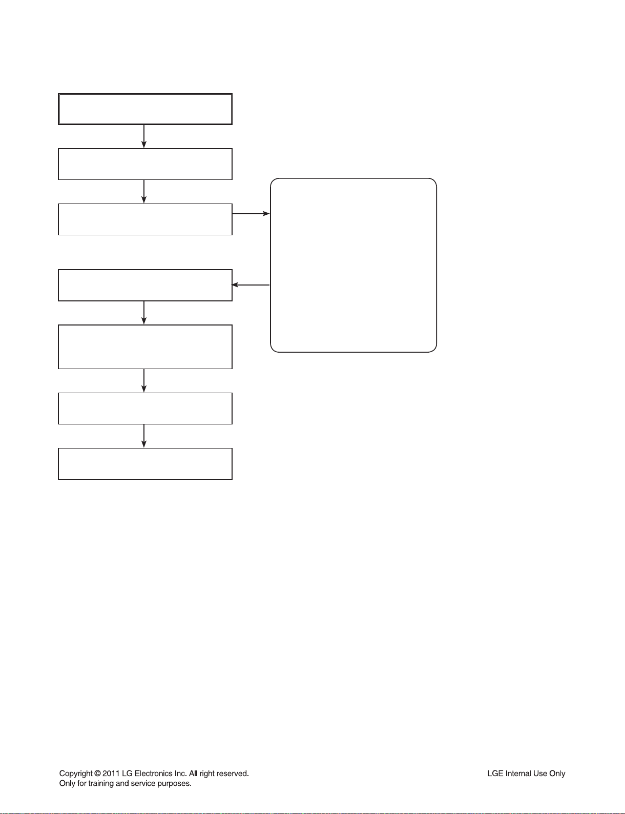
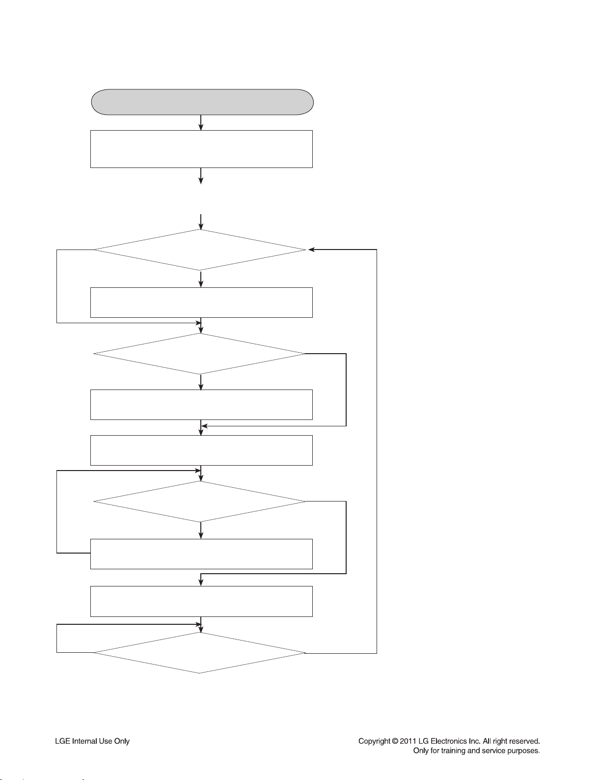
TROUBLESHOOTING GUIDE
1. Power Supply Circuit
INSERT POWER CORD.
YES
Turn power on.
YES
Is power on?
YES
Does it play?
YES
Does it output
audio?
YES
OK
NO
Check power supply circuit.
NO
Check tracking servo circuit.
NO
Check audio circuit.
2-1
Page 11
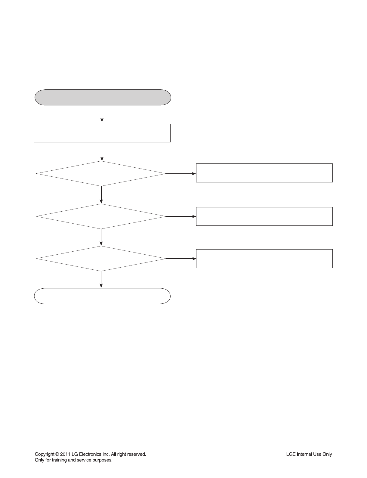
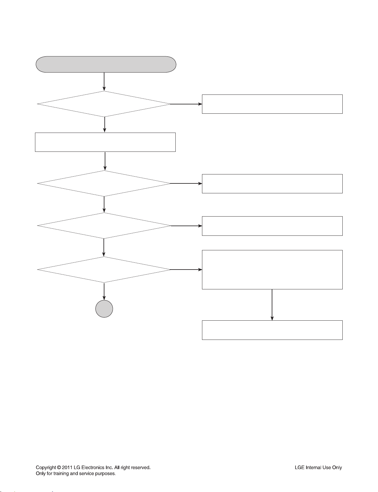
2. Front circuit (1/2)
POWER ON.
YES
Is the Digitron on
correctly?
YES
Check if all
buttons are ok?
YES
Check if the remote
control is ok?
YES
Front B/D ok.
NO
NO
NO
{
|
Check if
PN301 is ok?
YES
Check if the front
power is ok?
YES
Check if
DIS301 is ok?
NO
Reconnect it.
NO
Refer to SMPS part.
NO
Check pattern and resoldering
2-2
Page 12
3. Front circuit (2/2)
1
Check if the
power part of the
front is ok?
YES
Check if
R346~R349, R352, R370
ok?
YES
Refer to MICOM circuit.
2
NO
Refer to power(SMPS).
NO
Replace R346~R349, R352, R370.
Check if the
power part of the front
is ok?
YES
Check if the remote
control waveform of PN301
pin5 is ok?
YES
Check if RC301
voltage is ok(3.3V)?
YES
Resolder or Replace RC301.
NO
Refer to power(SMPS).
NO
Refer to MICOM circuit.
NO
Check RM circuit
2-3
Page 13
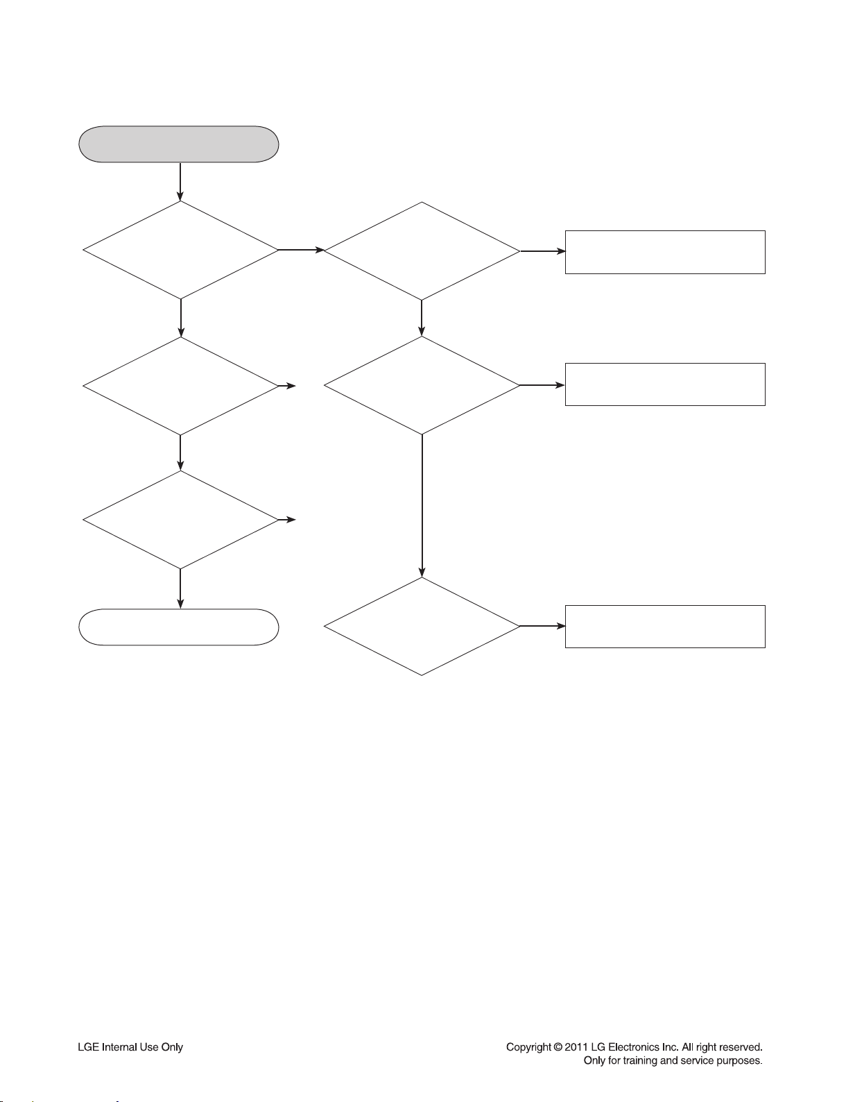
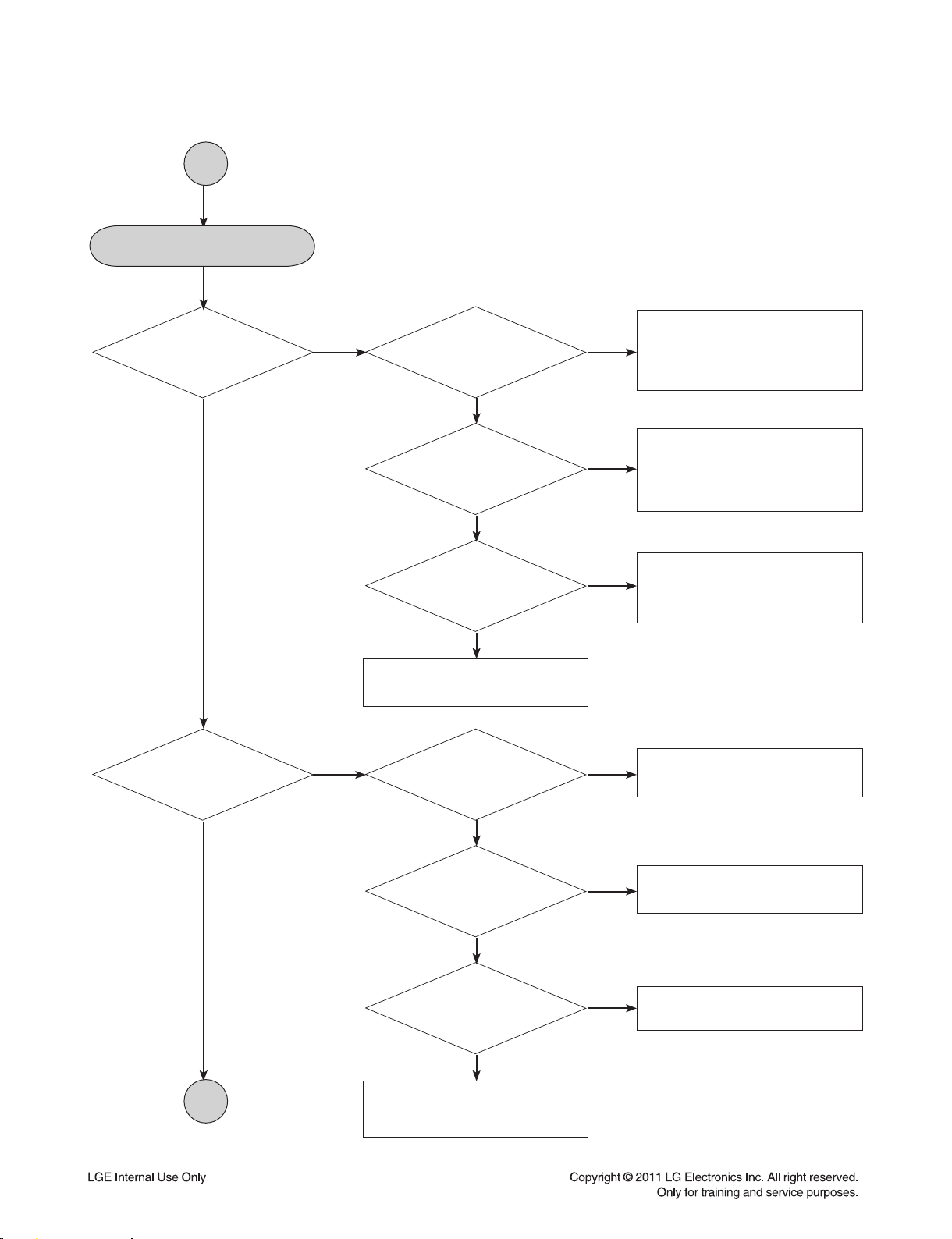
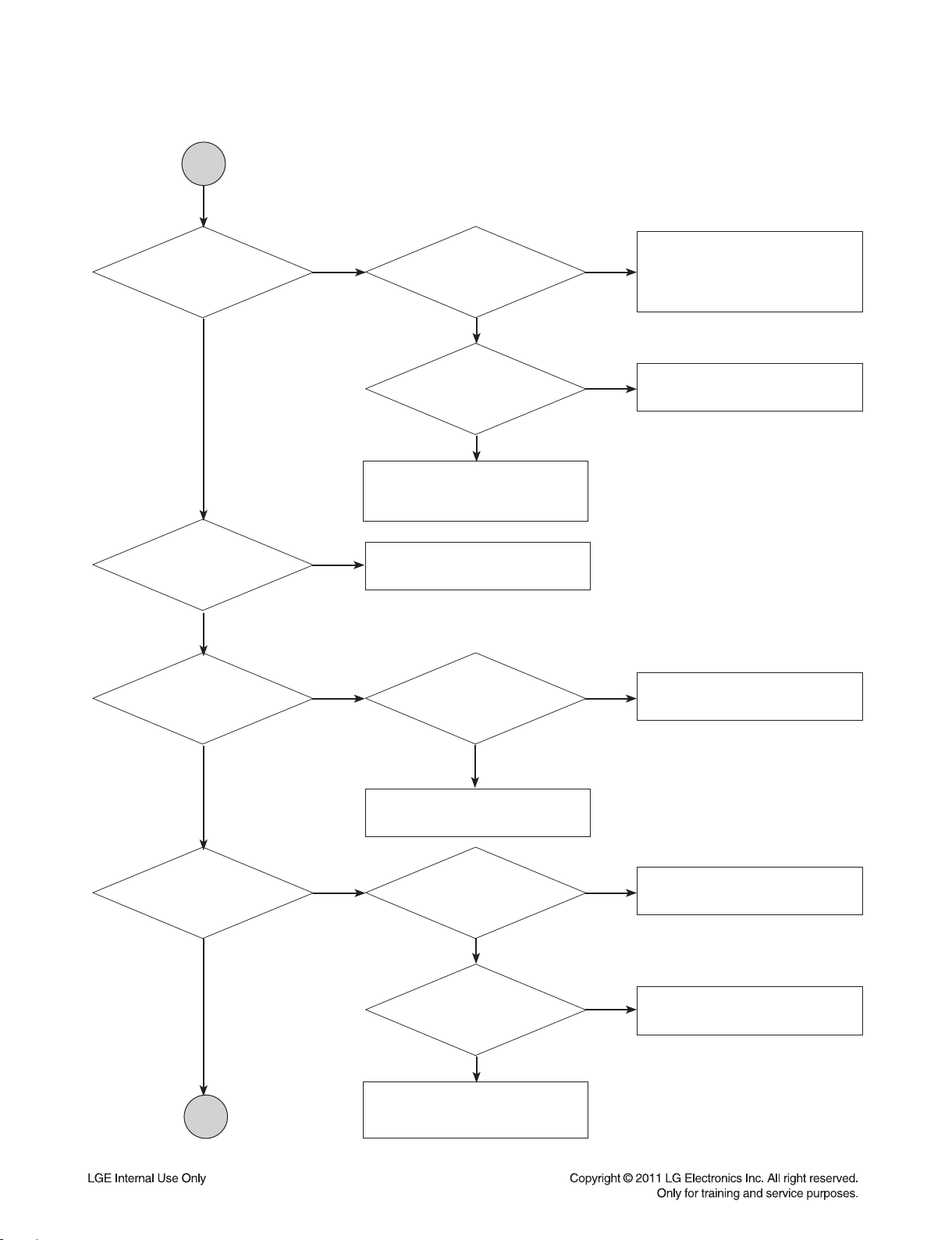
4. System operation flow
POWER ON.
1. Initializes SERVO, DSP & RISC registers.
2. Write RISC code to SDRAM.
3. Reset RISC.
Show LOGO.
YES
YES
Tray closed?
NO
Tray close to closed position.
SLED at inner
side?
NO
SLED moves to inner position.
1. Judge whether have disc and disc type.
2. Jump to related disc reading procedure.
Recieve
OPEN/ CLOSE
Key?
YES
YES
NO
NO
1. Execute Pressed Key & IR Key.
2. System operation routine loop.
1. Stop Playback & Open Tray.
2. Display tray open message & LOGO.
YES
Receive
CLOSE Key?
YES
2-4
Page 14
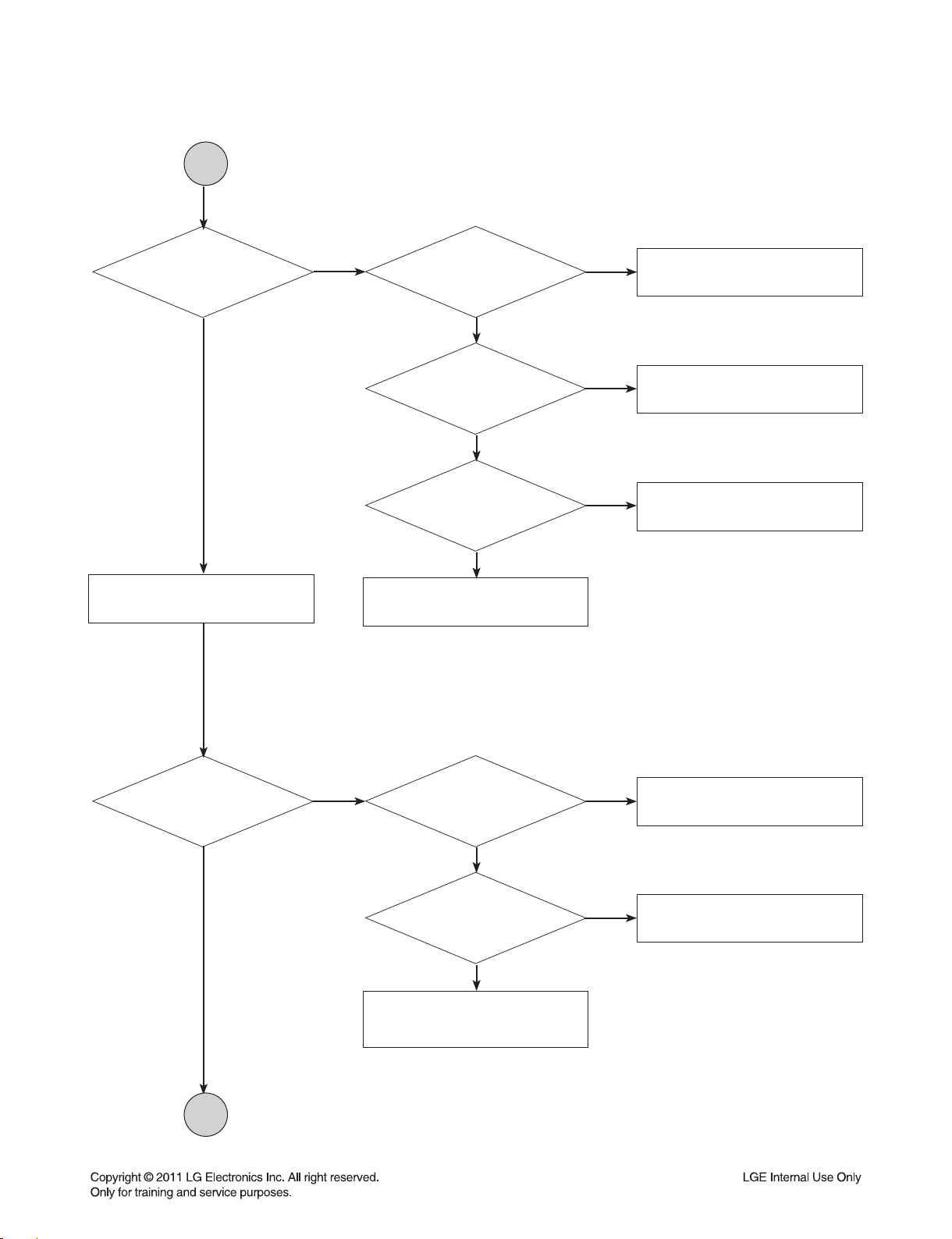
5. Test & debug flow
TEST.
YES
Check the
AC voltage Power PCBA (110V
or 220V).
YES
Switch on the Power PCBA.
YES
Are the
DC Voltage outputs OK? (12V,
3.3V, 5V, 7V, 34V).
YES
Are 3.3V and
5V DC outputs normal on main
PCBA?
YES
Update
FLASH successfully?
YES
NO
NO
NO
NO
Check the POWER PART.
Check the POWER PART.
Check the regulators or diode.
1. Check 27MHz system clock.
2. Check system reset circuit.
3. Check FLASH R/W enable signal PRD,
RWR.
4. Check FLASH Memory related circuit.
NO
A
Replace FLASH.
2-5
Page 15
A
YES
Power On.
YES
Show LOGO?
YES
Does Tray
move inside when it
is not at closed
position?
NO
NO
Flash
Memory operates
properly?
YES
SDRAM
works properly?
YES
MT1389L
VIDEO outputs
properly?
YES
Check AV cable
connection to TV set.
Normal
OPEN_SW,
CLOSE_SW
signal?
Check connection lines
NO
NO
NO
NO
between FLASH & MT1389L
and the FLASH access time
whether is suitable or not.
Check connection lines
between SDRAM(IC503) &
MT1389L and the SDRAM
is damaged.
Check the related circuit of
MT1389L IC501 Pins99, 102,
103, 104.
Check the load OPEN &
CLOSE switch.
B
YES
YES
Normal
TROPEN & TRCLOSE
signal?
YES
Normal
LOAD+ & LOAD-
signal?
YES
Check AV cable connection
between main PCBA and
loader. (MECHA)
2-6
NO
Check the Tray control IO pins
on MT1389L.
NO
Check the Tray control MOTOR
& SERVO circuit IC400.
Page 16
B
YES
Does
the SLED move to inner
side when it is at outer
position?
YES
Do not put in disc
and close tray.
NO
Motor
Driver M_STBY
pin is high?
YES
Motor
Driver M_STBY
pin is High?
YES
SLED+ and
SLED- output
properly?
YES
Check the cable connection
with MECHA.
NO
NO
NO
Check the connection line of
M_STBY.
Check the related circuit of
SLD.
Check the AMP circuit on
motor driver.
Optical Lens
has movements for
searching Focus?
YES
C
NO
Proper
Focus outputs
to motor driver?
YES
Proper F+ & F-
outputs?
YES
Check cable connection with
pick-up head.
2-7
NO
NO
Check Focus connection on
MT1389L and motor driver.
Check the AMP circuit on
motor driver.
Page 17
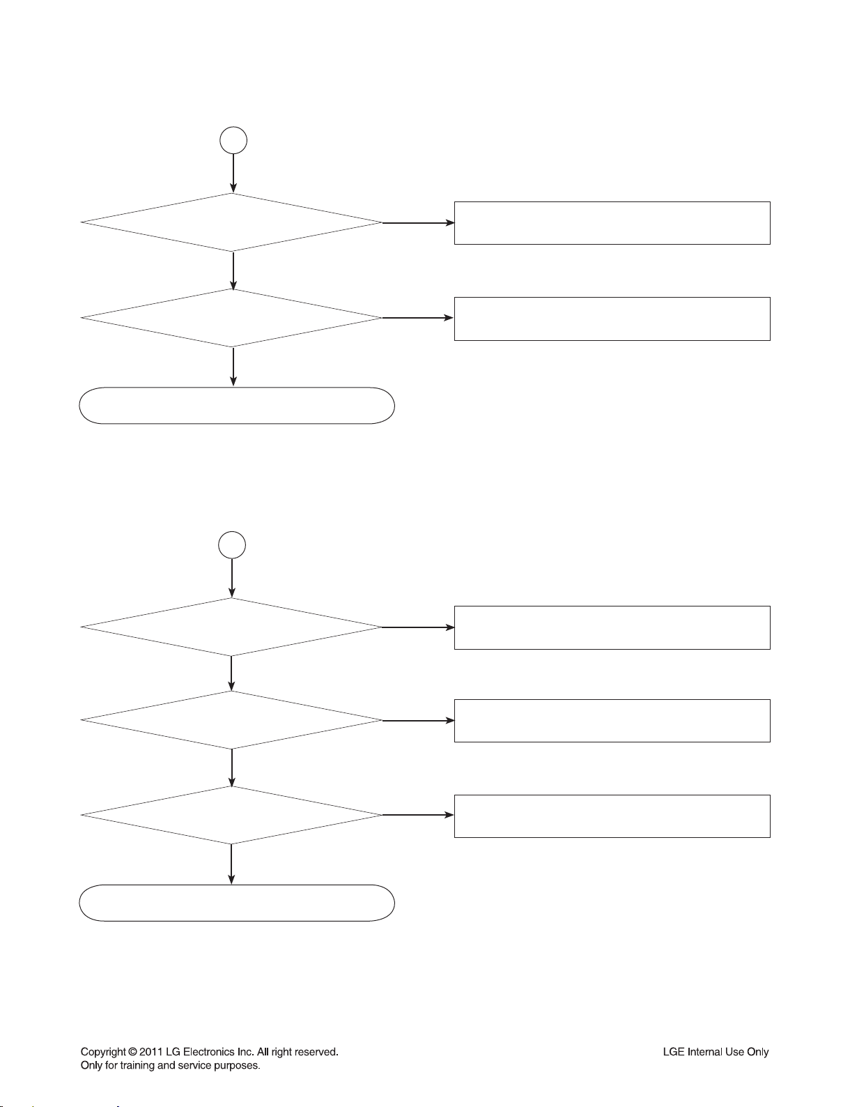
C
YES
Laser
turns on when
reading disc?
YES
Put disc in?
YES
Disc ID is correct?
NO
NO
NO
DVDLD or
CDLD output
property?
YES
Collector
voltage of power transistor
is OK?(Q403, Q405)
YES
Check cable connection
between transistor output and
pick-up head.
Laser off.
Proper
RF signal on
MT1389L.
NO
NO
NO
Check the laser power circuit
on MT1389L and
connecting to power
transistor(Q403, Q405).
Check the related circuit on
laser power transistor.
Check the related circuit on
MT1389L RF signal.
YES
Does spindle rotate?
YES
D
NO
YES
Check the RF connection
between AM5890 and
Proper
SPINDLE signal on
MT1389L.
SPNP
SPNN output
properly?
Check the cable connection
between spindle and main
PCB.
2-8
MT1389L
YES
YES
.
NO
NO
Check the SPINDLE related
circuit on MT1389L.
Check the spindle control AMP
circuit of motor driver.
Page 18
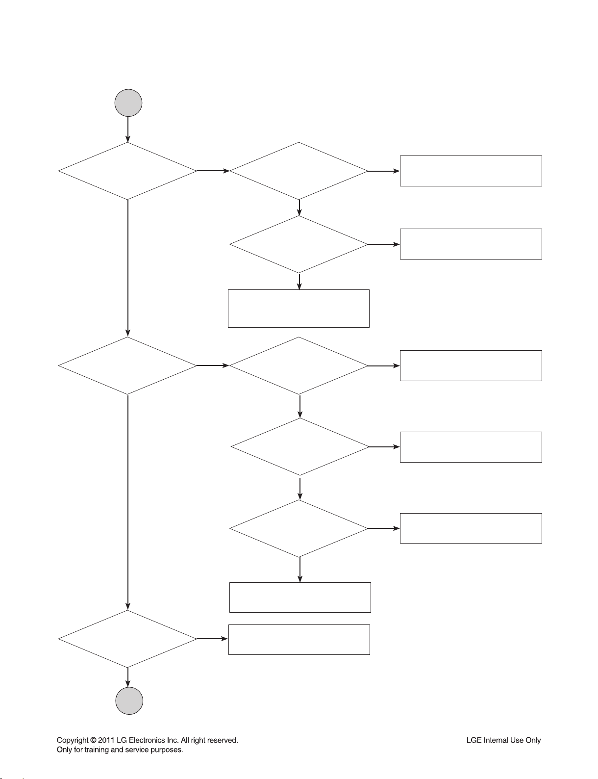
D
YES
Focus on ok?
YES
Track On OK?
YES
NO
NO
Proper
signals on A, B, C,
D of MT1389L.
YES
Proper
CD_DVDCT signal on
MT1389L.
YES
Check CD_DVDCT connection
between AM5890 and
MT1389L.
Proper
CD_DVDCT signal on
MT1389L.
YES
Proper
TRACK signal
on MT1389L.
NO
NO
NO
NO
Check connections between
MT1389L and pick-up head.
Check the related circuit on
MT1389L CD_DVDCT.
Check the related circuit on
MT1389L.
Check the TRACK connection
on
MT1389L
and motor driver.
Disc Playback?
YES
E
NO
YES
T+ & T- output
properly?
YES
Check cable connection
on pick-up head.
Check RF signal waveform.
2-9
NO
Check the tracking control AMP
circuit on motor driver.
Page 19
E
YES
Normal Audio
output when disc
playback?
YES
TEST END.
NO
PWM IC
received correct data
stream?
YES
Normal
PWM IC out?(IC602).
YES
Check Digital AMP circuit
(IC701, IC702).
NO
NO
Check connection between
IC602 BCK, LRCK, ADATA0.
Check the related circuit of
PWM.(Check Audio out
Pins28, 31, 33, 34, 37, 39, 42).
2-10
Page 20

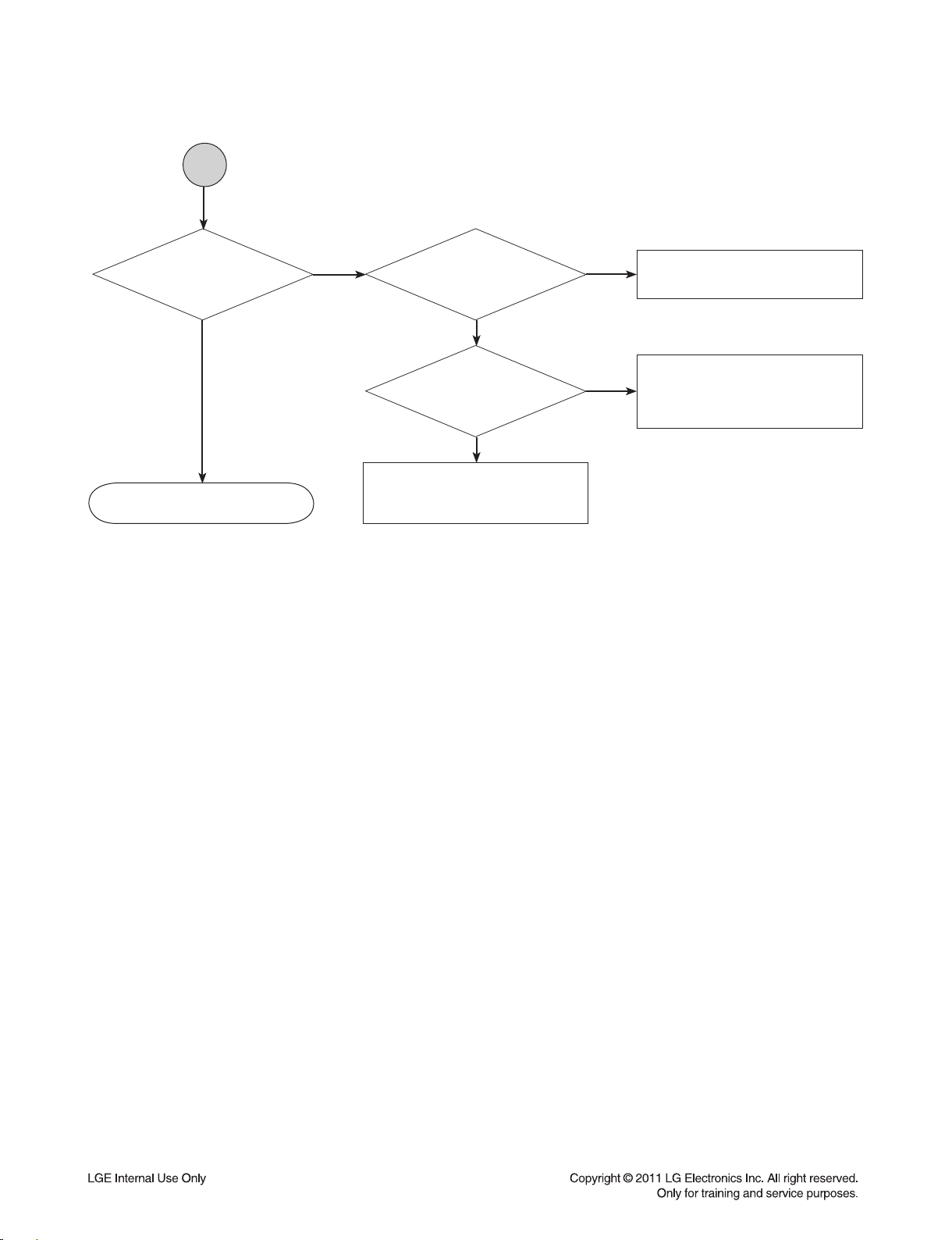
6. AMP Protection
"PROTECTION" appears on the FLD.
YES
After unplug power cord, connect again.
YES
Power on.
YES
"PROTECTION"
appears continuously on the FLD.
YES
Is the IC101 pin54
"LOW" signal(0V)?
YES
Is the Q701 and
Q702 normal?
YES
Replace TI AMP IC(IC701, IC702)
NO
OK.
NO
Replace IC101.
NO
Replace the Q701 and Q702.
2-11
Page 21

7. AUDIO μ-COM Circuit(DVD & AMP)
Power On.
YES
Does
CD/DVD appear at
FLD?
YES
Does
Reading appear
at FLD?
YES
Does
no Disc or Time
appear at
FLD?
YES
Check
if DVD and AUDIO
CD insert is
OK.
NO
NO
Does
it appear DVD Error
at FLD?
YES
Check
power part of Main
B/D.
YES
Check
oscillator of
X101.
YES
Does Aux,
Scart, opt and FM 87.5
appear at FLD.
NO
NO
Refer to SMPS.
NO
Refer to oscillator circuit.
YESNO
OK
NO
Check Power.
YES
Check DVD Module.
Check SMPS.
NO
Check
if IC101 Pin5
is high.
YES
Check
if IC101 Pin9,36,59 are
high(3.3V).
YES
Check
if IC101 Pin49
is high.
YES
Replace IC101.
NO
NO
NO
Check IC101 reset
waveform.
Check 3.3V line.
Check power section
2-12
circuit.
Page 22

DETAILS AND WAVEFORMS ON SYSTEM TEST AND DEBUGGING
1. SYSTEM 27MHz CLOCK,RESET,FLASH R/W SIGNAL
1)
MT1389L
2)
MT1389L
main clock is at 27MHz(X500)
FIG 1-1
reset is high active.
w G
1
19
20
1
21
12
38
2
40
39
k} kylzl{
24
y G
XU_}
16 26
10
11
YWW
ZUZ}
FIG 1-2
3
33
13
29
3
4
2
4
30
2-13
Page 23

3) Flash R/W enable signal during download(Downloading)
SF_DI
5
SF_DO
6
FIG 1-3
5
6
2. SDRAM CLOCK
1)
MT1389L
SDCLK
main clock is at 27MHz(X500)
DCLK = 93MHz, Vp-p=2.2, Vmax=2.7V
FIG 2-1
7
7
2-14
Page 24

3. TRAY OPEN/CLOSE SIGNAL
7
11
10
5
1) Tray open/close waveform
OPENSW
CLOSESW
OPEN
CLOSE
FIG 3-1
3) Tray open waveform
OPENSW
CLOSESW
2) Tray close waveform
OPENSW
8
CLOSESW
9
OPEN
10
CLOSE
11
FIG 3-2
8
18
28
8
9
10
11
17 22 2
OPEN
CLOSE
FIG 3-3
9
10
11
8
9
14
15
3
24
16 26
33
10
2818
11
17 22 27
30
34
3
2-15
Page 25

4. SLED CONTROL RELATED SIGNAL (NO DISC CONDITION)
0
33
SLD
12
M-STBY
13
1
19
20
SL+
SL-
FIG 4-1
14
15
24
10
3
16 26
11
12
21
33
30
13
29
38
39
4
10
11
18
28
17 22 27
30
34
35
8
2-16
9
14
15
Page 26

5. LENS CONTROL RELATED SIGNAL(NO DISC CONDITION)
3
0
1
FOD
F+
F-
FIG 5-1
16
17
18
18
24
10
28
3
16 26
11
17 22 27
33
3
34
6. LASER POWER CONTROL RELATED SIGNAL(NO DISC CONDITION)
19
12
20
21
MDI1
DVDLD
CDLD
19
20
FIG 6-1
21
2-17
38
39
40
Page 27

7. DISC TYPE JUDGEMENT WAVEFORMS
24
F+
PU_DET
RF
FIG 7-1 (DVD)
F+
PU_DET
22
23
24
22
23
16 26
33
10
11
28
18
8
9
14
23 : This signal can see using special debug program
17 22 27
15
34
39
37
23 25 32
36
30
35
FIG 7-2 (DVD)
RF
24
24
10
3
16 26
33
11
2-18
Page 28

F+
24
22
10
16 26
33
11
PU_DET
RF
F+
PU_DET
RF
FIG 7-3 (CD)
23
24
22
23
24
28
18
8
9
14
23 : This signal can see using special debug program
17 22 27
15
34
39
37
23 25 32
36
30
35
FIG 7-4 (CD)
2-19
24
10
3
16 26
33
11
Page 29

8. FOCUS ON WAVEFORMS
39
3
25 : This signal can see using special debug program
PU_DET
FOD
F+
F-
PU_DET
FOD
F+
F-
FIG 8-1 (DVD)
FIG 8-2 (CD)
25
26
27
28
25
26
27
28
18
24
10
28
37
23 25 32
3
16 26
11
17 22 27
36
33
30
34
8
9
14
15
2-20
Page 30

9. SPINDLE CONTROL WAVEFORMS (NO DISC CONDITION)
FIG 9-1
SPIND
SP-
SP+
24
10
29
30
31
3
16 26
11
13
33
29
18
28
17 22 27
30
34
31
35
8
9
14
15
2-21
Page 31

10. TRACKING CONTROL RELATED SIGNAL(System checking)
32 : This signal can see using special debug program
FIG 10-1(DVD)
PU_DET
TRO
T-
T+
PU_DET
TRO
T-
T+
32
33
34
35
32
33
34
35
39
37
23 25 32
36
FIG 10-2(CD)
24
10
2818
16 26
11
17 22 27
2-22
3
13
33
29
30
34
31
35
Page 32

11. MT1389L VIDEO OUTPUT WAVEFORMS
1) Full colorbar signal(COMPOSIT)
CVBS
36
FIG 11-1
39
37
23 25 32
36
2) Y
FIG 11-2
Y_G
37
39
37
23 25 32
36
2-23
Page 33

12. AUDIO OUTPUT FROM MT1389L
1) Audio related Signal
ASDATA3
FIG 12-1
ADATA0
BCK
LRCK
38
39
40
12
21
38
39
37
23 25 32
40
36
2-24
Page 34

13. DVD & AMP WAVEFORMS MT1389L
1)
• FL+ : R640
3)
• WF- : R642
or
WF+ : R643
5)
41
43
2)
42
• RL+ : R641
4)
44
• C+ : R644
6)
• FR+ : R645
45
46
2-25
45
46
• RR+ : R646
44
43
42
41
Page 35

2-26
Page 36

WIRING DIAGRAM
SMPS PCB
COMPONENT
CVBS
AUX
SCART
SPK TERMINAL
23PIN
9PIN
18PIN
14 PIN
12 PIN
MD
Tuner
JK202 JK201 TU100 JK701
MAIN+AMP PCB
FRONT PCB
USB/MIC PCB
VFD
VOLUME
MIC 1,2USB
PORT.IN
CN202
CN401
CN103
CN402
CN303
PN202
WIRING DIAGRAM
2009.11.24
2-27 2-28
Page 37

OVERALL BLOCK DIAGRAM
1/12
DVD_CLK
Tuner
LED
Clock
Driver
RMC
AMP IC+OPAMP
TAS5342DDV
DVD_RST
DVD_CE
DVD_DO
DVD_DI
RDS_DAT
RDS_CLK
TUNER_DAT
TUNER_CL
ST_IND
RCU_IN
KEY
PS9850
PWM_RST
PWMT_CLK
PWM_DAT
RESET
DBGP0
DBGP
DBGP2
D/L CNT
AMP_PDN
AMP_SD
AMP_PROTECT
MIC_DET
P_SENSE
SDRAM
SERIAL
FLASH
DSCK#,CKE,
CS0#,RAS0#
SF_CS, SF_DI,
SF_DO,SF_CLK
27MHZ
ADC
CS5346
V-JACK(4)
SCART
AUX_IN
(2)
MM1692
MOTOR
DRIVE
IC
(AM5890)
P/UP
M
DD
E
CK
M
ECHANIS
M
USB
CON
MIC
I/F
Portable IN
USBP,
USBN
S4308
MIC_L,R
A,B,C,D,E,F,RF
LDO1,LDO2
CD/DVDMDI
IOA,VRCD,VRDVD
OPEN/CLOSE
FOCUS/SLED
SPINDLE/TRACKIN
AMP_STBY
MPEG
MT1389L
(128PIN)
Y/G,PB/B,PR/R
CVBS
R/G/B
CVBS
Y/Pb/Pr
ADDATA
MCLK, LRCK,
BCK
ADC_RST
ADC_CLK
ADC_DAT
SANYO
LC87F564A
KEY
6965_DO
6965_CLK
6965_STB
POWER
I/F
3.7V
5V
LRCK,BCK,ADATA[0,2]
To PWM
From MPEG
Play-back ripping
:
128MBit(16MByte)
BLOCK DIAGRAM
2009.11.24
2-29 2-30
Page 38

A
1
2
3
4
5
6
7
8
9
10
11
12
BCDEFGH I J KLMNOPQRST
SMPS
EBY60688101 REV 4.3
2010. 12. 15
CIRCUIT DIAGRAMS
1. SMPS(POWER) CIRCUIT DIAGRAM
NOTES) Symbol denotes AC ground.
NOTES) Symbol denotes DC chassis ground.
NOTE) Warning
NOTE) Parts that are shaded are critical
NOTE) With respect to risk of fire or
NOTE) electricial shock.
CAUTION:
Danger if fuse is incorrectly replaced.
Replace only with the type identical to fuse rating
and(or) model name described in main label.
2-31 2-32
IMPORTANT SAFETY NOTICE
WHEN SERVICING THIS CHASSIS, UNDER NO
CIRCUMSTANCES SHOULD THE ORIGINAL DESIGN BE
MODIFIED OR ALTERED WITHOUT PERMISSION
FROM THE LG CORPORATION. ALL COMPONENTS
SHOULD BE REPLACED ONLY WITH TYPES IDENTICAL
TO THOSE IN THE ORIGINAL CIRCUIT. SPECIAL
COMPONENTS ARE SHADED ON THE SCHEMATIC
FOR EASY IDENTIFICATION.
THIS CIRCUIT DIAGRAM MAY OCCASIONALLY DIFFER
FROM THE ACTUAL CIRCUIT USED. THIS WAY,
IMPLEMENTATION OF THE LATEST SAFETY AND
PERFORMANCE IMPROVEMENT CHANGES INTO
THE SET IS NOT DELAYED UNTIL THE NEW SERVICE
LITERATURE IS PRINTED.
NOTE :
1. Shaded(
) parts are critical for safety. Replace only
with specified part number.
2. Voltages are DC-measured with a digital voltmeter
during Play mode.
Page 39

12
35
21
7
40
36
16 26
17 22 27
15
13
29
31
9
11
6
20
19
23 25332
1
5
38
24
33
30
34
10
28
14
8
18
39
37
A
1
2
3
4
5
6
7
8
9
10
11
12
BCDEFGH I J KLMNOPQRST
MAIN&
EBY60708001(#01) REV 2.8
2010. 12. 15
2. MAIN & AMP - 1 CIRCUIT DIAGRAM
WAVEFORM
2-33 2-34
Page 40

3. MAIN & AMP - 2 CIRCUIT DIAGRAM
2
44
43
42
41
45
46
4
A
1
2
3
4
5
6
7
8
9
10
11
12
BCDEFGH I J KLMNOPQRST
MAIN&
EBY60708001(#02) REV 2.8
2010. 12. 15
WAVEFORM
2-35 2-36
Page 41

4. FRONT CIRCUIT DIAGRAM
A
1
2
3
4
5
6
7
8
9
10
11
12
BCDEFGH I J KLMNOPQRST
FRONT
EBY60687401 REV 2.2
2009.11.24
2-37 2-38
Page 42

5. FRONT JACK CIRCUIT DIAGRAM
A
1
2
3
4
5
6
7
8
9
10
11
12
BCDEFGH I J KLMNOPQRST
FRONT JACK
EBY60687501 REV 2.4
2009.12.22
2-39 2-40
Page 43

CIRCUIT VOLTAGE CHART
1. ICs ON MAIN AND AMP BOARD
Location Pin No. Spec. EE Mode(V) Margin
Playback
Mode(V)
Margin
IC101 MICOM (LC87F5M64A)
9(VDD2) 2.8~5.5 3.4 0.6 3.4 0.6
36(VDD3) 2.8~5.6 3.4 0.6 3.4 0.6
59(VDD1) 2.8~5.7 3.4 0.6 3.4 0.6
IC201 ADC
5(VLC) 3.1~5.0~5.25 4.95 0.3 4.97 0.28
14(VA) 3.1~5.0~5.25 4.94 0.31 4.93 0.32
36(VLS) 3.1~3.3~5.25 3.34 1.91 3.34 1.91
46(VD) 3.1~3.3~5.25 3.34 1.91 3.34 1.91
IC204 SCART IC
1(VCC) 4.5~5.5 4.93 0.43 4.92 0.42
IC400 MOTOR
8(VCC1) 4.3~13.2 4.95 0.65 4.91 0.61
19(VCC2) 4.3~VCC 4.95 0.65 4.9 0.6
IC501 MPEG (MT1389L)
7 (AVDD18_2) 1.7~2.0 1.86 0.14 1.9 0.1
8 (AVDD33_1) 3.0~3.6 3.19 0.19 3.21 0.21
19 (AVDD33_2) 3.0~3.6 3.19 0.19 3.21 0.21
29 (VDD33_USB) 3.0~3.6 3.21 0.21 3.19 0.19
32 (VDD18_USB) 1.7~2.0 1.84 0.14 1.9 0.1
50 (DVDD33) 3.0~3.6 3.21 0.21 3.19 0.19
54 (DVDD18) 1.7~2.0 1.86 0.14 1.9 0.1
68(DVDD33) 3.0~3.6 3.21 0.21 3.19 0.19
84 (DVDD33) 3.0~3.6 3.21 0.21 3.19 0.19
90 (DVDD18) 1.7~2.0 1.86 0.14 1.9 0.1
95(DACVDDC) 3.0~3.6 3.19 0.19 3.18 0.18
100(DACVDDB) 3.0~3.6 3.19 0.19 3.18 0.18
101(DACVDDA) 3.0~3.6 3.19 0.19 3.18 0.18
109(AADVDD) 3.0~3.6 3.16 0.16 3.16 0.16
110(APLLVDD) 3.0~3.6 3.17 0.17 3.16 0.16
121(ADACVDD1) 3.0~3.6 3.22 0.22 3.22 0.22
122(ADACVDD2) 3.0~3.6 3.22 0.22 3.22 0.22
123(AVDD18_1) 1.7~2.0 1.86 0.14 1.91 0.09
IC502 FLASH
8(VDD) 2.3~3.6 3.21 0.39 3.19 0.41
IC503 SDRAM
1(VDD1) 3.0~3.6 3.21 0.39 3.19 0.41
3(VDDQ3) 3.0~3.6 3.21 0.39 3.31 0.29
9(VDDQ9) 3.0~3.6 3.21 0.39 3.31 0.29
14(VDD14) 3.0~3.6 3.21 0.39 3.31 0.29
27(VDD27) 3.0~3.6 3.21 0.39 3.31 0.29
43(VDDQ43) 3.0~3.6 3.21 0.39 3.31 0.29
49(VDDQ49) 3.0~3.6 3.21 0.39 3.31 0.29
IC504 EEPROM
8(VCC)
1.8~5.5(Read)
2.7~5.5(write)
3.41 2.09 3.4 2.1
Location Pin No. Spec. EE Mode(V) Margin
Playback
Mode(V)
Margin
IC602 PWM (PS9850)
16(VDD_IO) - 3.24 - 3.24 -
24(VDD_IO) - 3.24 - 3.24 -
29(VDD_IO) - 3.24 - 3.24 -
32(VDD_IO) - 3.24 - 3.24 -
35(VDD_IO) - 3.24 - 3.24 -
40(VDD_IO) - 3.24 - 3.24 -
48(VDD_IO) - 3.24 - 3.24 -
61(VDD_VIN2) - 3.24 - 3.24 -
64(VDD_VIN1) - 3.24 - 3.24 -
IC701 AMP
1(GVDD) 10.8~13.2 12.11 1.09 12.11 1.09
21(VDD) 10.8~13.2 12.11 1.09 12.11 1.09
22(GVDD) 10.8~13.2 12.11 1.09 12.11 1.09
23(GVDD) 10.8~13.2 12.11 1.09 12.11 1.09
26(PVDD_D) 0~31.5~34 33.8 0.2 33.8 0.2
27(PVDD_D) 0~31.5~34 33.8 0.2 33.8 0.2
32(PVDD_C) 0~31.5~34 33.8 0.2 33.8 0.2
35(PVDD_B) 0~31.5~34 33.8 0.2 33.8 0.2
40(PVDD_A) 0~31.5~34 33.8 0.2 33.8 0.2
41(PVDD_A) 0~31.5~34 33.8 0.2 33.8 0.2
IC702 AMP
1(GVDD) 10.8~13.2 12.11 1.09 12.11 1.09
21(VDD) 10.8~13.2 12.11 1.09 12.11 1.09
22(GVDD) 10.8~13.2 12.11 1.09 12.11 1.09
23(GVDD) 10.8~13.2 12.11 1.09 12.11 1.09
26(PVDD_D) 0~31.5~34 33.8 0.2 33.8 0.2
27(PVDD_D) 0~31.5~34 33.8 0.2 33.8 0.2
32(PVDD_C) 0~31.5~34 33.8 0.2 33.8 0.2
35(PVDD_B) 0~31.5~34 33.8 0.2 33.8 0.2
40(PVDD_A) 0~31.5~34 33.8 0.2 33.8 0.2
41(PVDD_A) 0~31.5~34 33.8 0.2 33.8 0.2
2. ICs ON FRONT BOARD
Location Pin No. Spec. EE Mode(V) Margin
Playback
Mode(V)
Margin
IC301 VFD IC
13(VDD) 4.5~5.5 3.42 -1.08 3.41 -1.09
30(VEE) VDD-35 -20.6 10.98 -20.4 11.19
43(VDD) 4.5~5.6 3.42 -1.08 3.41 -1.09
2-41 2-42
Page 44

3. CAPACITORS ON MAIN AND AMP BOARD
4. CAPACITORS ON FRONT BOARD
No.
Capacitor
Value(uF)
Voltage
Spec.
EE Mode Playback
(+) (-) Gap Margin (+) (-) Gap Margin
C106 220 10 V 3.41 V 0 V 3.41 V 6.59 V 3.4 V 0 V 3.4 V 6.6 V
C114 100 16 V 3.4 V 0 V 3.4 V 12.6 V 3.4 V 0 V 3.4 V 12.6 V
C122 220 10 V 3.69 V 0 V 3.69 V 6.31 V 3.69 V 0 V 3.69 V 6.31 V
C124 47 16 V 4.96 V 0 V 4.96 V 11.04 V 4.95 V 0 V 4.95 V 11.05 V
C127 47 16 V 12.11 V 0 V 12.11 V 3.89 V 12.12 V -0.01 V 12.13 V 3.87 V
C133 47 16 V 3.4 V 0 V 3.4 V 12.6 V 3.4 V 0 V 3.4 V 12.6 V
C145 10 16 V 3.4 V 0 V 3.4 V 12.6 V 3.39 V 0 V 3.39 V 12.61 V
C146 100 16 V 3.24 V 0 V 3.24 V 12.76 V 3.24 V 0 V 3.24 V 12.76 V
C241 22 50 V 2.47 V 0 V 2.47 V 47.53 V 2.46 V 0 V 2.46 V 47.54 V
C243 47 16 V 4.93 V 0 V 4.93 V 11.07 V 4.92 V 0 V 4.92 V 11.08 V
C264 10 16 V 4.94 V 0 V 4.94 V 11.06 V 4.93 V 0 V 4.93 V 11.07 V
C265 10 16 V 3.24 V 0 V 3.24 V 12.76 V 3.24 V 0 V 3.24 V 12.76 V
C267 47 16 V 4.92 V 0 V 4.92 V 11.08 V 4.92 V 0 V 4.92 V 11.08 V
C268 10 16 V 2.46 V 0 V 2.46 V 13.54 V 2.46 V 0 V 2.46 V 13.54 V
C274 470 10 V 1.57 V 1.4 V 0.17 V 9.83 V 2.13 V 1.93 V 0.2 V 9.8 V
C275 470 10 V 2.29 V 2.21 V 0.08 V 9.92 V 2.29 V 2.09 V 0.2 V 9.8 V
C276 470 10 V 2.28 V 2.14 V 0.14 V 9.86 V 2.28 V 2.11 V 0.17 V 9.83 V
C282 470 10 V 1.56 V 0.89 V 0.67 V 9.33 V 2.1 V 1.41 V 0.69 V 9.31 V
C417 47 16 V 3.21 V 3.2 V 0.01 V 15.99 V 3.19 V 2.28 V 0.91 V 15.09 V
C418 47 16 V 3.21 3.2 V 0.01 V 15.99 V 3.19 V 3.02 V 0.17 V 15.83 V
C420 47 16 V 4.95 V 0 V 4.95 V 11.05 V 4.9 V 0.04 V 4.86 V 11.14 V
C421 47 16 V 4.95 V 0 V 4.95 V 11.05 V 4.91 V 0.04 V 4.87 V 11.13 V
C423 100 16 V 4.94 0 V 4.94 V 11.06 V 4.93 V 0 V 4.93 V 11.07 V
C426 47 16 V 2.02 V 0 V 2.02 V 13.98 V 2.03 V 0 V 2.03 V 13.97 V
C427 47 16 V 1.41 V 0 V 1.41 V 14.59 V 1.41 V 0.04 V 1.37 V 14.63 V
C451 47 16 V 1.89 V 0 V 1.89 V 14.11 V 1.94 V 0.04 V 1.9 V 14.1 V
C506 47 16 V 3.21 V 0 V 3.21 V 12.79 V 3.19 V 0 V 3.19 V 12.81 V
C508 47 16 V 1.84 0 V 1.84 V 14.16 V 1.9 V 0 V 1.9 V 14.1 V
C516 47 16 V 3.19 0 3.19 V 12.81 V 3.18 V 0 V 3.18 V 12.82 V
C520 47 16 V 1.34 V 0 V 1.34 V 14.66 V 1.34 0.02 1.32 V 14.68 V
C523 220 10 V 3.16 V 0 V 3.16 V 6.84 V 3.16 0 3.16 V 6.84 V
C532 100 10 V 3.17 V 0 V 3.17 V 6.83 V 3.16 V 0 V 3.16 V 6.84 V
C538 10 16 V 1.47 V 0 V 1.47 V 14.53 V 1.58 V 0 V 1.58 V 14.42 V
C549 220 10 V 3.22 V 0 V 3.22 V 6.78 V 3.22 V 0 V 3.22 V 6.78 V
C563 10 16 V 3.21 V 0 V 3.21 V 12.79 V 3.19 V 0 V 3.19 V 12.81 V
C565 10 16 V 3.21 V 0 V 3.21 V 12.79 V 3.2 V 0 V 3.2 V 12.8 V
C613 10 16 V 1.24 V 0 V 1.24 V 14.76 V 1.24 V 0 V 1.24 V 14.76 V
C648 10 16 V -0.02 V -0.06 V 0.04 V 15.96 V -0.01 V -0.03 V 0.02 V 15.98 V
C702 47 50 V 12.11 V -0.04 V 12.15 V 37.85 V 12.11 V -0.02 V 12.13 V 37.87 V
C708 10 16 V 12 V 0.01 V 11.99 V 4.01 V 12.08 V -0.03 V 12.11 V 3.89 V
C723 470 50 V 33.8 V 0 V 33.8 V 16.2 V 33.8 V 0 V 33.8 V 16.2 V
C729 470 50 V 33.8 V 16.8 V 17 V 33 V 33.8 V 16.8 V 17 V 33 V
C730 470 50 V 16.8 V 0 V 16.8 V 33.2 V 16.8 V 0 V 16.8 V 33.2 V
C731 470 50 V 16.8 V 0 V 16.8 V 33.2 V 16.8 V 0 V 16.8 V 33.2 V
C732 470 50 V 33.8 V 16.8 V 17 V 33 V 33.8 V 16.8 V 17 V 33 V
C746 470 50 V 33.8 V 0 V 33.8 V 16.2 V 33.8 V 0 V 33.8 V 16.2 V
No.
Capacitor
Value(uF)
Voltage
Spec.
EE Mode Playback
(+) (-) Gap Margin (+) (-) Gap Margin
C753 10 16 V 12.07 V -0.03 V 12.1 V 3.9 V 12.08 V -0.03 V 12.11 V 3.89 V
C768 470 50 V 33.8 V 16.8 V 17 V 33 V 33.8 V 16.8 V 17 V 33 V
C770 470 50 V 16.8 V 0 V 16.8 V 33.2 V 16.8 V 0 V 16.8 V 33.2 V
C782 470 50 V 33.8 V 16.8 V 17 V 33 V 33.8 V 16.8 V 17 V 33 V
C784 470 50 V 16.8 V 0 V 16.8 V 33.2 V 16.8 V 0 V 16.8 V 33.2 V
C785 470 50 V 33.8 V 16.8 V 17 V 33 V 33.8 V 16.8 V 17 V 33 V
C7A7 470 50 V 33.8 V 0 V 33.8 V 16.2 V 33.8 V 0 V 33.8 V 16.2 V
C7A8 470 50 V 33.8 V 0 V 33.8 V 16.2 V 33.8 V 0 V 33.8 V 16.2 V
C800 10 16 V 1.22 V 1.15 V 0.07 V 15.93 V 1.31 V 2.03 V -0.72 V 16.72 V
No.
Capacitor
Value(uF)
Voltage
Spec.
EE Mode Playback
(+) (-) Gap Margin (+) (-) Gap Margin
C229 100 16 V 11.5 V 0 V 11.5 V 4.5 V 11.49 V 0 V - -
C2A3 220 16 V 2 V 0 V 2 V 14 V 2 V 0 V - -
C2A7 1 50 V 0 V 0 V 0 V 50 V 0 V 0 V - -
C2D1 220 6.3 V 4.97 V 0.04 V 4.93 V 1.37 V 4.95 V 0 V - -
C2D3 4.7 50 V 0.56 V 0.18 V 0.38 V 49.62 V 0.5 V 0.05 V - -
C2D4 4.7 50 V 0.9 V 0.5 V 0.4 V 49.6 V 0.82 V 0.37 V - -
C309 220 6.3 V 3.33 V 0 V 3.33 V 2.97 V 3.32 V 0 V - -
C332 47 35 V 18.12 V 0 V 18.12 V 16.88 V 17.9 V 0 V - -
C333 47 35 V 0 V 0 V 0 V 35 V 0 V 0 V - -
C3A1 47 16 V 3.42 V 0 V 3.42 V 12.58 V 3.4 V 0 V - -
C3A2 47 35 V 0 V -20.6 V 20.6 V 14.4 V 0 V -20.4 V - -
2-43 2-44
Page 45

PRINTED CIRCUIT BOARD DIAGRAMS
1. MAIN P.C. BOARD DIAGRAM (TOP VIEW)
2-45 2-46
Page 46

MAIN P.C. BOARD DIAGRAM (BOTTOM VIEW)
2-47 2-48
Page 47

2. SMPS P.C. BOARD DIAGRAM
2-49 2-50
NOTE: Warning
Parts that are shaded are critical With
respect to risk of fire or electrical shock.
Page 48

3. FRONT P.C BOARD DIAGRAM (TOP VIEW)
FRONT P.C BOARD DIAGRAM (BOTTOM VIEW)
4. FRONT JACK P.C. BOARD DIAGRAM (TOP VIEW)
FRONT JACK P.C. BOARD DIAGRAM (BOTTOM VIEW)
2-51 2-52
Page 49

2-53 2-54
Page 50

A
B
E
C
A
B
D
C
A43
A50
463
463
463
A46
300
471
262
263
261
260
261
A44
465
462
250
A41
PN202
284
284
283
282
463
CABLE1
D
E
A47
463
SMPS
MAIN
FRONT
JACK
279
• CABINET AND MAIN FRAME SECTION
SECTION 3. EXPLODED VIEWS
3-1 3-2
NOTES) THE EXCLAMATION POINT WITHIN AN
EQUILATERAL TRIANGLE IS INTENDED
TO ALERT THE SERVICE PERSONNEL
TO THE PRESENCE OF IMPORTANT
SAFETY INFORMATION IN SERVICE
LITERATURE.
Page 51

• DECK MECHANISM EXPLODED VIEW (DP-15T)
3-3 3-4
001
A02
017
013
435
015
439
018
015B
015A
014
002
003
A01
020
016
026
A03
019
440
012
442
037
012
010
012A
442
Page 52

• PACKING ACCESSORY SECTION
811 Video Cable
808 Battery
900 Remote Control
804 Bag
824 AM Loop Antenna
825 FM Antenna
801 Owner’s Manual
803 Packing
802 Box
803A Speaker Packing
803B Speaker Packing
803C Speaker Packing
3-5
Page 53

• SPEAKER SECTION
1. FRONT/REAR/CENTER SPEAKER (SH36SD-S)
A800 Front SPK
A600 Rear SPK
A700 Center SPK
852
854
850A
850B
851
853
WIRE80 Front SPK Wire (3M)
WIRE70 Center SPK Wire (3M)
WIRE60 Rear SPK Wire (7M)
3-6
Page 54

2. PASSIVE SUBWOOFER (SH36SD-W)
A900
3-7
Page 55

3-8
Page 56

SECTION 4. MECHANISM (DP-15T)
[CONTENTS]
DECK MECHANISM PARTS LOCATIONS
• Top View . . . . . . . . . . . . . . . . . . . . . . . . . . . . . . . . . . . . . . . . . . . . . . . . . . . . . . . . . . . . . . . 4-2
• Top View(without Tray Disc) . . . . . . . . . . . . . . . . . . . . . . . . . . . . . . . . . . . . . . . . . . . . . . 4-2
• Bottom View . . . . . . . . . . . . . . . . . . . . . . . . . . . . . . . . . . . . . . . . . . . . . . . . . . . . . . . . . . . . 4-2
DECK MECHANISM DISASSEMBLY
1. Main Base . . . . . . . . . . . . . . . . . . . . . . . . . . . . . . . . . . . . . . . . . . . . . . . . . . . . . . . . . . . . . 4-3
1-1. Clamp Assembly Disc . . . . . . . . . . . . . . . . . . . . . . . . . . . . . . . . . . . . . . . . . . . . . . . . . 4-3
1-1-1. Plate Clamp. . . . . . . . . . . . . . . . . . . . . . . . . . . . . . . . . . . . . . . . . . . . . . . . . . . . 4-3
1-1-2. Magnet Clamp . . . . . . . . . . . . . . . . . . . . . . . . . . . . . . . . . . . . . . . . . . . . . . . . . . 4-3
1-1-3. Clamp Upper . . . . . . . . . . . . . . . . . . . . . . . . . . . . . . . . . . . . . . . . . . . . . . . . . . . 4-3
2. Tray Disc . . . . . . . . . . . . . . . . . . . . . . . . . . . . . . . . . . . . . . . . . . . . . . . . . . . . . . . . . . . . . . 4-3
3. Base Assembly Sled . . . . . . . . . . . . . . . . . . . . . . . . . . . . . . . . . . . . . . . . . . . . . . . . . . . . 4-4
3-1. Gear Feed . . . . . . . . . . . . . . . . . . . . . . . . . . . . . . . . . . . . . . . . . . . . . . . . . . . . . . . . . . 4-4
3-2. Gear Middle . . . . . . . . . . . . . . . . . . . . . . . . . . . . . . . . . . . . . . . . . . . . . . . . . . . . . . . . . 4-4
3-3. Gear Rack . . . . . . . . . . . . . . . . . . . . . . . . . . . . . . . . . . . . . . . . . . . . . . . . . . . . . . . . . . 4-4
4. Rubber Rear . . . . . . . . . . . . . . . . . . . . . . . . . . . . . . . . . . . . . . . . . . . . . . . . . . . . . . . . . . . 4-4
5. Frame Assembly Up/Down . . . . . . . . . . . . . . . . . . . . . . . . . . . . . . . . . . . . . . . . . . . . . . . 4-5
6. Belt Loading . . . . . . . . . . . . . . . . . . . . . . . . . . . . . . . . . . . . . . . . . . . . . . . . . . . . . . . . . . . 4-5
7. Gear Pulley . . . . . . . . . . . . . . . . . . . . . . . . . . . . . . . . . . . . . . . . . . . . . . . . . . . . . . . . . . . . 4-5
8. Gear Loading . . . . . . . . . . . . . . . . . . . . . . . . . . . . . . . . . . . . . . . . . . . . . . . . . . . . . . . . . . 4-5
9. Guide Up/Down . . . . . . . . . . . . . . . . . . . . . . . . . . . . . . . . . . . . . . . . . . . . . . . . . . . . . . . . 4-5
10. PWB Assembly Loading . . . . . . . . . . . . . . . . . . . . . . . . . . . . . . . . . . . . . . . . . . . . . . . . 4-5
11. Base Main . . . . . . . . . . . . . . . . . . . . . . . . . . . . . . . . . . . . . . . . . . . . . . . . . . . . . . . . . . . . 4-5
EXPLODED VIEW
1. DECK MECHANISM EXPLODED VIEW (DP-15T) . . . . . . . . . . . . . . . . . . . . . . . . . . . . . . 4-6
4-1
Page 57

DECK MECHANISM PARTS LOCATIONS
• Top View
• Top View(without Tray Disc)
• Bottom View
Procedure
Starting No.
1
1
1, 2
1, 2, 3
1, 2, 3, 4
1
1, 6
1, 2, 6
1, 2, 6, 8
1, 2, 6, 8, 9
1, 2, 7
1, 2, 7
1, 2
1, 2 ,13
1, 2, 13, 14
1, 2, 7, 12,
13, 14
1, 2, 13
1, 2, 7, 12, 13,
14, 15, 16, 17
2
3
4
5
6
7
8
9
10
11
12
13
14
15
16
17
18
Parts Fixing Type
Main Base
Clamp Assembly
Disc
Plate Clamp
Magnet Clamp
Clamp Upper
Tray Disc
Base Assembly Sled
Gear Feed
Gear Middle
Gear Rack
Rubber Rear
Frame Assembly
Up/Down
Belt Loading
Gear Pulley
Gear Loading
Guide Up/Down
PWB Assembly
Loading
Base Main
4 Screws,
1 Connector
1 Locking Tabs
1 Screw
1 Screw
1 Locking Tab
1 Locking Tab
1 Locking Tab
1 Hook
2 Screw
2 Locking Tabs
Disass
embly
Bottom
Bottom
Fig-
ure
4-1
4-1
4-1
4-1
4-1
4-2
4-3
4-3
4-3
4-3
4-3
4-4
4-4
4-4
4-4
4-4
4-4
4-4
4-2
Note
When reassembling, perform the procedure in
reverse order.
The “Bottom” on Disassembly column of above
Table indicates the part should be disassembled
at the Bottom side.
Page 58

PLATE CLAMP
MAGNET CLAMP
CLAMP UPPER
DECK MECHANISM DISASSEMBLY
TRAY DISC
MAIN BASE
DISC CLAMP ASSEMBLY
HOLDER
(Fig. A)
BASE MAIN
1. Main Base (Fig. 4-1)
1-1. Clamp Assembly Disc
1) Place the Clamp Assembly Disc as Fig. (A)
2) Lift up the Clamp Assembly Disc in direction of
arrow(A).
3) Separate the Clamp Assembly Disc from the
Holder Clamp.
1-1-1. Plate Clamp
1) Turn the Plate Clamp to counterclockwise
direction and then lift up the Plate Clamp.
1-1-2. Magnet Clamp
1-1-3. Clamp Upper
BASE MAIN
LEVER
BASE MAIN
BOTTOM SIDE VIEW
Fig. 4-2Fig. 4-1
2. Tray Disc (Fig. 4-2)
1) Insert and push a Driver in the emergency eject
hole(A) at the right side, or put the Driver on the
Lever(B) of the Gear Emergency and pull the
Lever(B) in direction of arrow so that the Tray
Disc is ejected about 15~20mm.
2) Pull the Tray Disc until it is separated from the
Base Main completely.
4-3
Page 59

RUBBER DAMPER
RUBBER DAMPER
Distinguish upper and
lower sides
(Assemble with care)
RUBBER DAMPER
Distinguish upper and
lower sides
(Assemble with care)
BASE PU
GENERAL PICK UP ASSEMBLY
GEAR RACK
SPINDLE MOTOR ASSEMBLY
3. Base Assembly Sled (Fig. 4-3)
1) Release 4 Screw(S2).
2) Disconnect the FFC Connector(C1)
3-1. Gear Feed
3-2. Gear Middle
3-3. Gear Rack
(S2)
(S2)
RUBBER DAMPER
Fig. 4-3
4. Rubber Rear (Fig. 4-3)
4-4
Page 60

GEAR LOADING
GUIDE UP/DOWN
SCREW INSERTION
TORGUE CONTROL
(800gf DOWN)
GUIDE UP/DOWN
GEAR PULLEY
(L4)
BELT LOADING
(A)
(L5)
FIG. (A)
PWB ASSEMBLY LOADING
BASE MAIN
(B)
(C)
(B)
FIG. (C)
(S5)
(A)
GUIDE UP/DOWN
Fig. 4-4
(H1)
(C2)
(A)
(B)
FIG. (B)
GUIDE UP/DOWN
(L6)
(L6)
BASE MAIN
(S4)
(S4)
UP/DOWN FRAME ASSEMBLY
5.
Frame Assembly Up/Down (Fig. 4-4)
Note
Put the Base Main face down(Bottom Side)
1) Release the screw(S4)
2) Unlock the Locking Tab(L3) in direction of arrow
and then lift up the Frame Assembly Up/Down to
separate it from the Base Main.
Note
• When reassembling move the Guide Up/Down
in direction of arrow(C) until it is positioned as
Fig.(C).
• When reassembling insert (A) portion of the Frame
Assembly Up/Down in the (B) portion of the Guide
Up/Down as Fig.(B)
6. Belt Loading(Fig. 4-4)
Note
Put the Base Main on original position(Top Side)
7. Gear pulley (Fig. 4-4)
1) Unlock the Locking Tab(L4) in direction of arrow(B) and
then separate the Gear Pulley from the Base Main.
8. Gear Loading (Fig. 4-4)
9. Guide Up/Down (Fig. 4-4)
1) Move the Guide Up/Down in direction of arrow(A) as
Fig.(A)
2) Push the Locking Tab(L5) down and then lift up the
Guide Up/Down to separate it from the Base Main.
Note
When reassembling place the Guide Up/Down as Fig.(C)
and move it in direction arrow(B) until it is locked by the
Locking Tab(L5). And confirm the Guide Up/Down as Fig.(A)
10. PWB Assembly Loading
(Fig. 4-4)
Note
Put the Base Main face down(Bottom Side)
1) Release 1 Screws(S5)
2) Unlock the Loading Motor (C2) from the Hook (H1) on
the Base Main.
3) Unlock 2 Locking Tabs(L6) and separate the PWB
Assembly Loading from the Base Main.
11. Base Main(Fig. 4-4)
4-5
Page 61

DECK MECHANISM EXPLODED VIEW (DP-15T)
001
A02
017
013
435
015
439
018
015B
015A
014
002
003
A01
020
016
026
A03
019
4-6
440
012
442
037
012
010
012A
442
 Loading...