

Page 1

LCD PROJECTION TV
SERVICE MANUAL
CAUTION
BEFORE SERVICING THE CHASSIS,
READ THE SAFETY PRECAUTIONS IN THIS MANUAL.
CHASSIS : NB-03JA
MODEL : RU-52SZ30 RU-60SZ30
website:http://biz.LGservice.com
e-mail:http://www.LGEservice.com/techsup.html
Page 2

CONTENTS . . . . . . . . . . . . . . . . . . . . . . . . . . . . . . . . . . . . . . . . . . . . . . . . . . . . . . 2
SAFETY PRECAUTIONS . . . . . . . . . . . . . . . . . . . . . . . . . . . . . . . . . . . . . . . . . . . . 3
SERVICING PRECAUTIONS. . . . . . . . . . . . . . . . . . . . . . . . . . . . . . . . . . . . . . . . . . 4
ELECTROSTATICALLY SENSITIVE (ES) DEVICES . . . . . . . . . . . . . . . . . . . . . . . . 4
DESCRIPTION OF CONTROLS . . . . . . . . . . . . . . . . . . . . . . . . . . . . . . . . . . . . . . . 5
SPECIFICATION . . . . . . . . . . . . . . . . . . . . . . . . . . . . . . . . . . . . . . . . . . . . . . . . . . 12
ADJUSTMENT INSTRUCTIONS . . . . . . . . . . . . . . . . . . . . . . . . . . . . . . . . . . . . . . 13
REPLACING THE LAMP. . . . . . . . . . . . . . . . . . . . . . . . . . . . . . . . . . . . . . . . . . . . 19
BLOCK DIAGRAM. . . . . . . . . . . . . . . . . . . . . . . . . . . . . . . . . . . . . . . . . . . . . . . . . 20
EXPLODED VIEW. . . . . . . . . . . . . . . . . . . . . . . . . . . . . . . . . . . . . . . . . . . . . . 24, 26
EXPLODED VIEW PARTS LIST . . . . . . . . . . . . . . . . . . . . . . . . . . . . . . . . . . . . 25,27
REPLACEMENT PARTS LIST. . . . . . . . . . . . . . . . . . . . . . . . . . . . . . . . . . . . . . . . 28
SCHEMATIC DIAGRAM . . . . . . . . . . . . . . . . . . . . . . . . . . . . . . . . . . . . . . . . . . . . . .
- 2 -
Page 3
- 3 -
SAFETY PRECAUTIONS
1.5 Kohm/10W
To Instrument's
exposed
METALLIC PARTS
Good Earth Ground
such as WATER PIPE,
CONDUIT etc.
AC Volt-meter
IMPORTANT SAFETY NOTICE
Many electrical and mechanical parts in this chassis have special safety-related characteristics. These parts are identified by in
the Schematic Diagram and Replacement Parts List.
It is essential that these special safety parts should be replaced with the same components as recommended in this manual to
prevent X-RADIATION, Shock, Fire, or other Hazards.
Do not modify the original design without permission of manufacturer.
General Guidance
An lsolation Transformer should always be used during
the servicing of a receiver whose chassis is not isolated from
the AC power line. Use a transformer of adequate power rating
as this protects the technician from accidents resulting in
personal injury from electrical shocks.
It will also protect the receiver and it's components from being
damaged by accidental shorts of the circuitary that may be
inadvertently introduced during the service operation.
If any fuse (or Fusible Resistor) in this TV receiver is blown,
replace it with the specified.
When replacing a high wattage resistor (Oxide Metal Film
Resistor, over 1W), keep the resistor 10mm away from PCB.
Keep wires away from high voltage or high temperature parts.
Due to high vacuum and large surface area of picture tube,
extreme care should be used in handling the Picture Tube.
Do not lift the Picture tube by it's Neck.
Before returning the receiver to the customer,
always perform an AC leakage current check on the exposed
metallic parts of the cabinet, such as antennas, terminals, etc.,
to be sure the set is safe to operate without damage of
electrical shock.
Leakage Current Cold Check(Antenna Cold Check)
With the instrument AC plug removed from AC source,
connect an electrical jumper across the two AC plug prongs.
Place the AC switch in the on positioin, connect one lead of
ohm-meter to the AC plug prongs tied together and touch other
ohm-meter lead in turn to each exposed metallic parts such as
antenna terminals, phone jacks, etc.
If the exposed metallic part has a return path to the chassis, the
measured resistance should be between 1MΩ and 5.2MΩ.
When the exposed metal has no return path to the chassis the
reading must be infinite.
An other abnormality exists that must be corrected before the
receiver is returned to the customer.
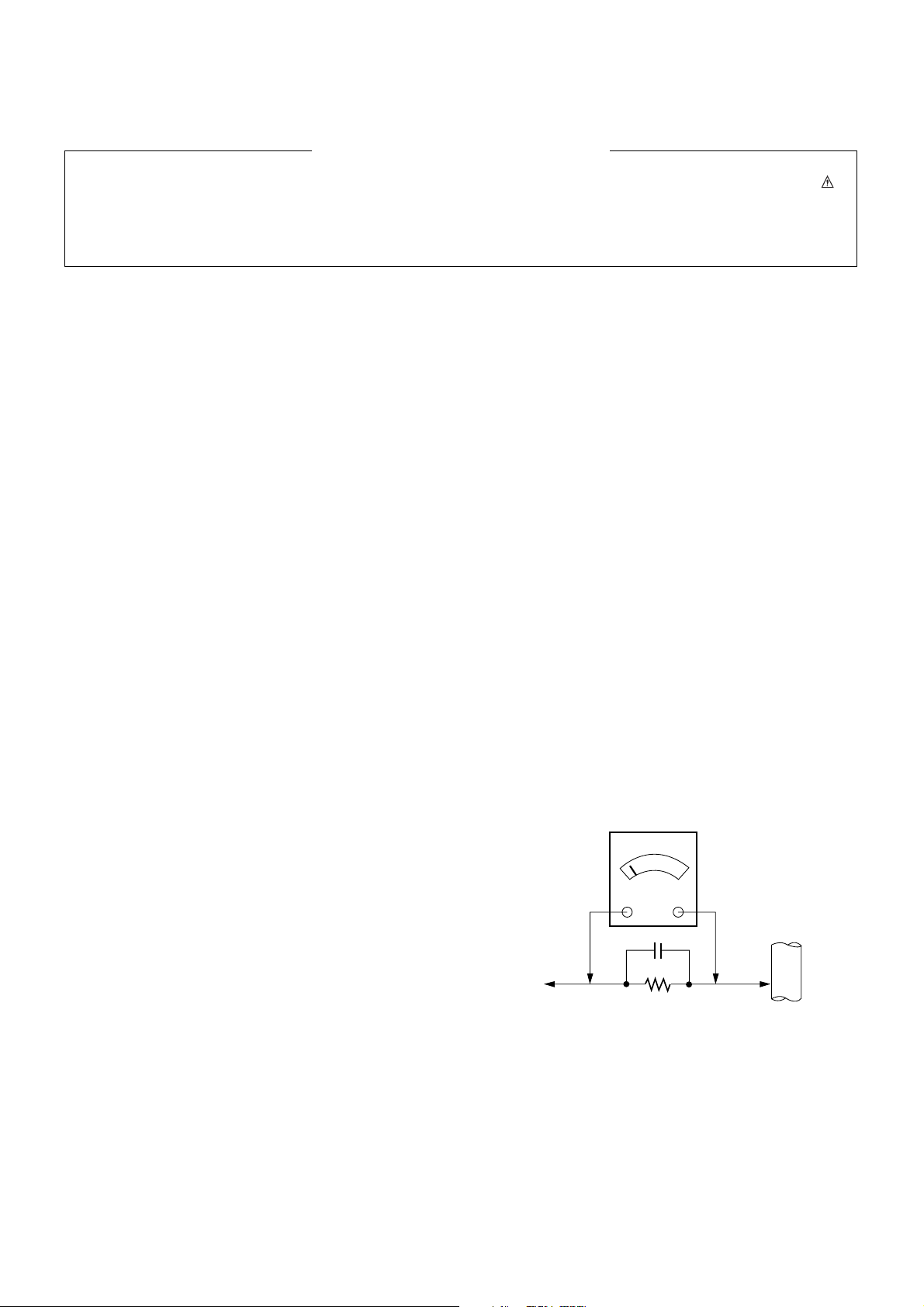
Leakage Current Hot Check (See below Figure)
Plug the AC cord directly into the AC outlet.
Do not use a line Isolation Transformer during this check.
Connect 1.5K/10watt resistor in parallel with a 0.15uF capacitor
between a known good earth ground (Water Pipe, Conduit, etc.)
and the exposed metallic parts.
Measure the AC voltage across the resistor using AC
voltmeter with 1000 ohms/volt or more sensitivity.
Reverse plug the AC cord into the AC outlet and repeat AC
voltage measurements for each esposed metallic part. Any
voltage measured must not exceed 0.75 volt RMS which is
corresponds to 0.5mA.
In case any measurement is out of the limits sepcified, there is
possibility of shock hazard and the set must be checked and
repaired before it is returned to the customer.
Leakage Current Hot Check circuit
0.15uF
Page 4

SERVICING PRECAUTIONS
- 4 -
CAUTION: Before servicing instruments covered by this service manual and
its supplements, read and follow the SAFETY PRECAUTIONS section of this
manual. Note: If unforeseen circumstances create conflict between the following servicing precautions and any of the safety precautions, always follow the
safety precautions. Remember: Safety First.
General Servicing Precautions
1. a. Always unplug the instrument AC power cord from the AC power source
before: (1) removing or reinstalling any component, circuit board, module,
or any other instrument assembly. (2) disconnecting or reconnecting any
instrument electrical plug or other electrical connections. (3) connecting a
test substitute in parallel with an electrolytic capacitor in the instrument.
Caution: A wrong part substitution or incorrect polar-ity installation of
electrolytic capacitors may result in an explosion hazard.
b. Do not defeat any plug/socket B+ voltage interlocks with which instru-
ments covered by this service manual might be equipped.
c. Do not apply AC power to this instrument and/or any of its electrical
assemblies unless all solid-state device heat sinks are correctly installed.
d. Always connect a test instrument’s ground lead to the instrument chassis
ground before connecting the test instrument positive lead.
Always remove the test instrument ground lead last.
Note: Refer to the Safety Precautions section of this manual.
2. The service precautions are indicated or printed on the cabinet, chassis, or
components. When servicing, follow the printed or indicated service precautions and service materials.
3. The components used in the unit have a specified flame resistance and
dielectric strength. When replacing any components, use components
which have the same ratings. Components identified by shading, by
*
, or
by in the circuit diagram are important for safety or for the characteristics
of the unit. Always replace with the exact replacement components.
4. An insulation tube or tape is sometimes used and some components are
raised above the printed wiring board for safety. The internal wiring is sometimes clamped to prevent contact with heating components. Install them as
they were.
5. After servicing, always check that the removed screws, components, and
wiring have been installed correctly and that the portion around the service
part have not been damaged. Further, check the insulation between the
blades of the attachment plug and accessible conductive parts.
INSULATION CHECKING PROCEDURE
Disconnect the attachment plug from the AC outlet and turn the power on.
Connect the insulation resistance meter (500 V) to the blades of the attachment plug. The insulation resistance between each blade of the attachment
plug and accessible conductive parts (Note 1) should be more than 1 Mohm.
Note: Accessible conductive parts include metal panels, input terminals, earphone jacks, etc.
ELECTROSTATICALLY SENSITIVE (ES) DEVICES
Some semiconductor (solid-state) devices can be damaged easily by static electricity. Such components commonly are called
Electrostatically Sensitive (ES) Devices. Examples of typical ES
devices are integrated circuits and some field-effect transistors
and semiconductor “chip” components. The following techniques
should be used to help reduce the incidence of component damage caused by static electricity.
1. Immediately before handling any semiconductor component
or semiconductor-equipped assembly, drain off any electrostatic charge on the body by touching a known earth ground.
Alternatively, obtain and wear a commercially available discharging wrist strap device, which should be removed for
potential shock reasons prior to applying power to the unit
under test.
2. After removing an electrical assembly equipped with ES
devices, place the assembly on a conductive surface such as
aluminum foil, to prevent electrostatic charge buildup or exposure of the assembly.
3. Use only a grounded-tip soldering iron to solder or unsolder
ES devices.
4. Use only an anti-static solder removal device. Some solder
removal devices not classified as “anti-static” can generate
electrical charges sufficient to damage ES devices.
5. Do not use freon-propelled chemicals. These can generate
electrical charge sufficient to damage ES devices.
6. Do not remove a replacement ES device from its protective
package until immediately before you are ready to install
t.(Most replacement ES devices are packaged with leads electrically shorted together by conductive foam, aluminum foil, or
comparable conductive material.)
7. Immediately before removing the protective material from the
leads of a replacement ES device, touch the protective material to the chassis or circuit assembly into which the device will
be installed.
Caution: Be sure no power is applied to the chassis or circuit,
and observe all other safety precautions.
8. Minimize bodily motions when handling unpackaged replace
ment ES devices. (Otherwise, seemingly harmless motion,
such as the brushing together of your clothing or the lifting of
your foot from a carpeted floor, can generate static electricity
sufficient to damage an ES device.)
Page 5
- 5 -
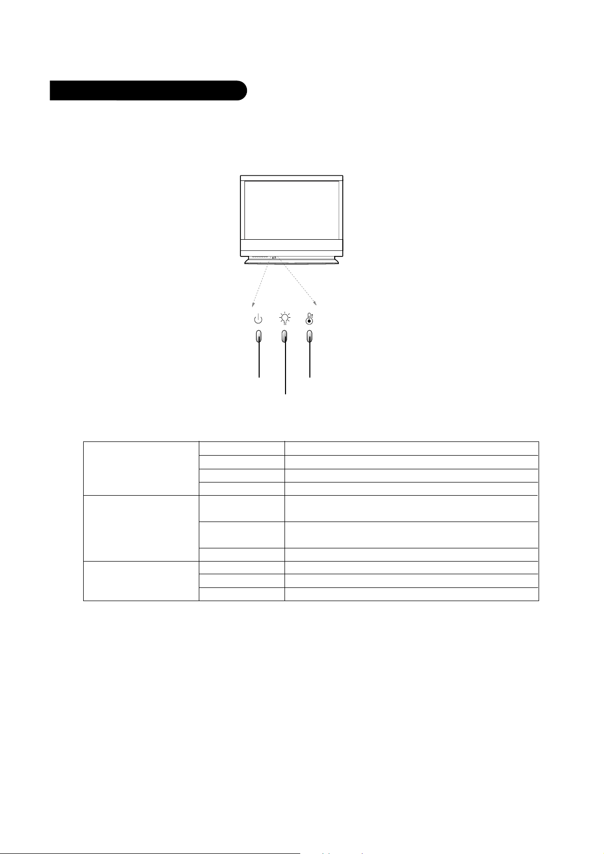
DESCRIPTION OF CONTROLS
Function Status Indicators
Lamp indicator, operation indicator, and temperature indicator located below the front panel
controls, reveal the operating status of the LCD projection TV.
Operation Indicator
Lamp Indicator
Temperature Indicator
Operation Indicator
Lamp Indicator
Temperature Indicator
Off Power cord is not connected.
Red Power Cord is connected, TV is in standby mode.
Green On
Orange (flashing) Preparing operation in standby mode.
Orange Projection lamp is reaching the end of its life and needs to
be replaced with a new lamp.
Red (flashing) There is a problem with the lamp or around it. Contact an
authorized service center.
Green (flashing) The lamp cover is not closed.
Orange The projection TV is overheating.
Red The projection TV shut down due to overheating.
Red (flashing) The projection TV shut down, check the cooling fan.
Page 6
- 6 -
On-Screen Displays
10
AM 03:00
TV 13
MONO
TV 6
This page describes your on-screen display and information banner options.
Main Channel Display
Displays current channel number.
Channel Label
If a channel label has been
set, then it will appear here.
PIP Display
This display
appears when
ABC
PIP is active.
Mute
Appears
when sound
is muted.
Volume
Volume level is displayed while
adjusting the sound.
Time
Appears when
pressing the
enter button on
remote control.
Page 7
- 7 -
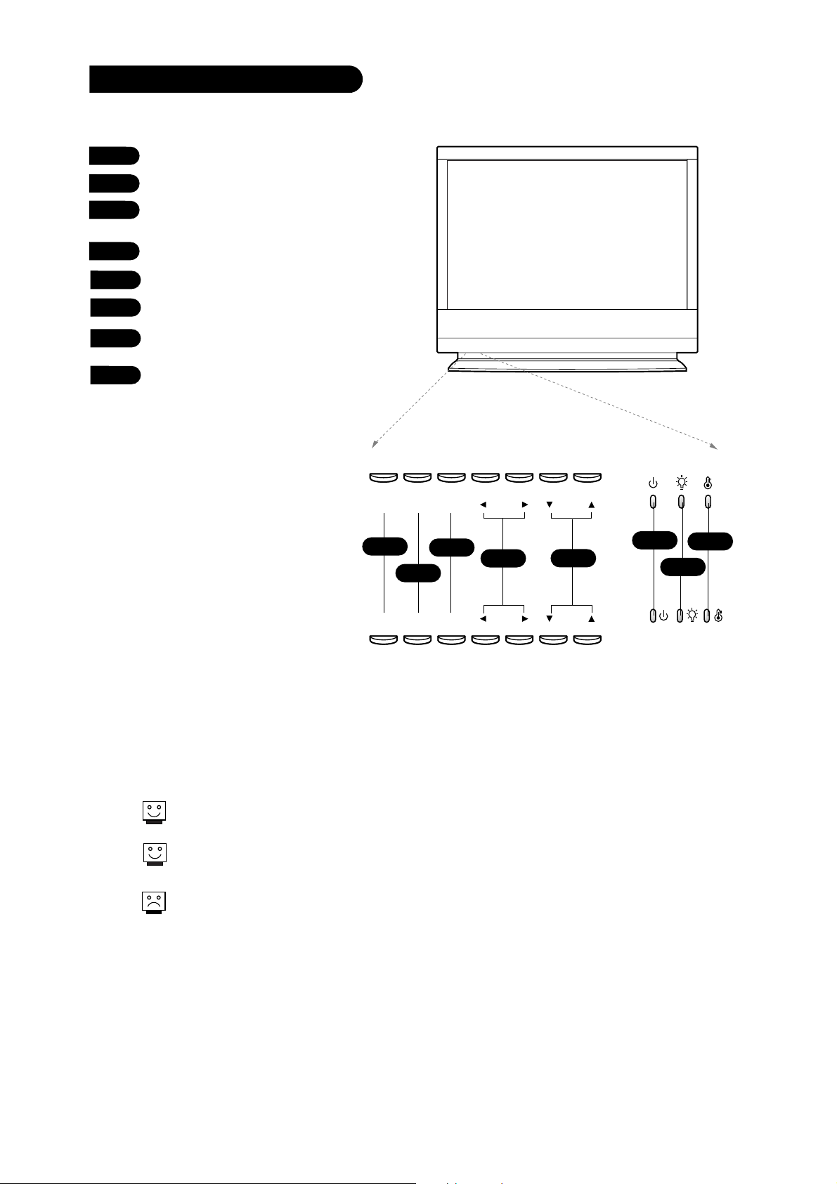
Front Panel Controls
power menu enter vol ch
power menu enter vol ch
1
2
3
4
5
6
7
8
Power On / Off
Menu
Enter (Same as ENTER button on
your remote control)
VOLUME UP / DOWN
CHANNEL UP / DOWN
Operation indicator.
Lamp indicator.
Temperature indicator.
RU-52SZ30
1
3
4
5
6
2
8
7
See menu pages for instructions on using the
on-screen menus.
The POWER, CHANNEL and VOLUME buttons
work just as they do on your remote control.
Don’t turn TV on after placing TV from low temperature to normal temperature. It may cause humidity of
inside TV. Try it again after about 3 hours.
RU-60SZ30
Page 8
- 8 -
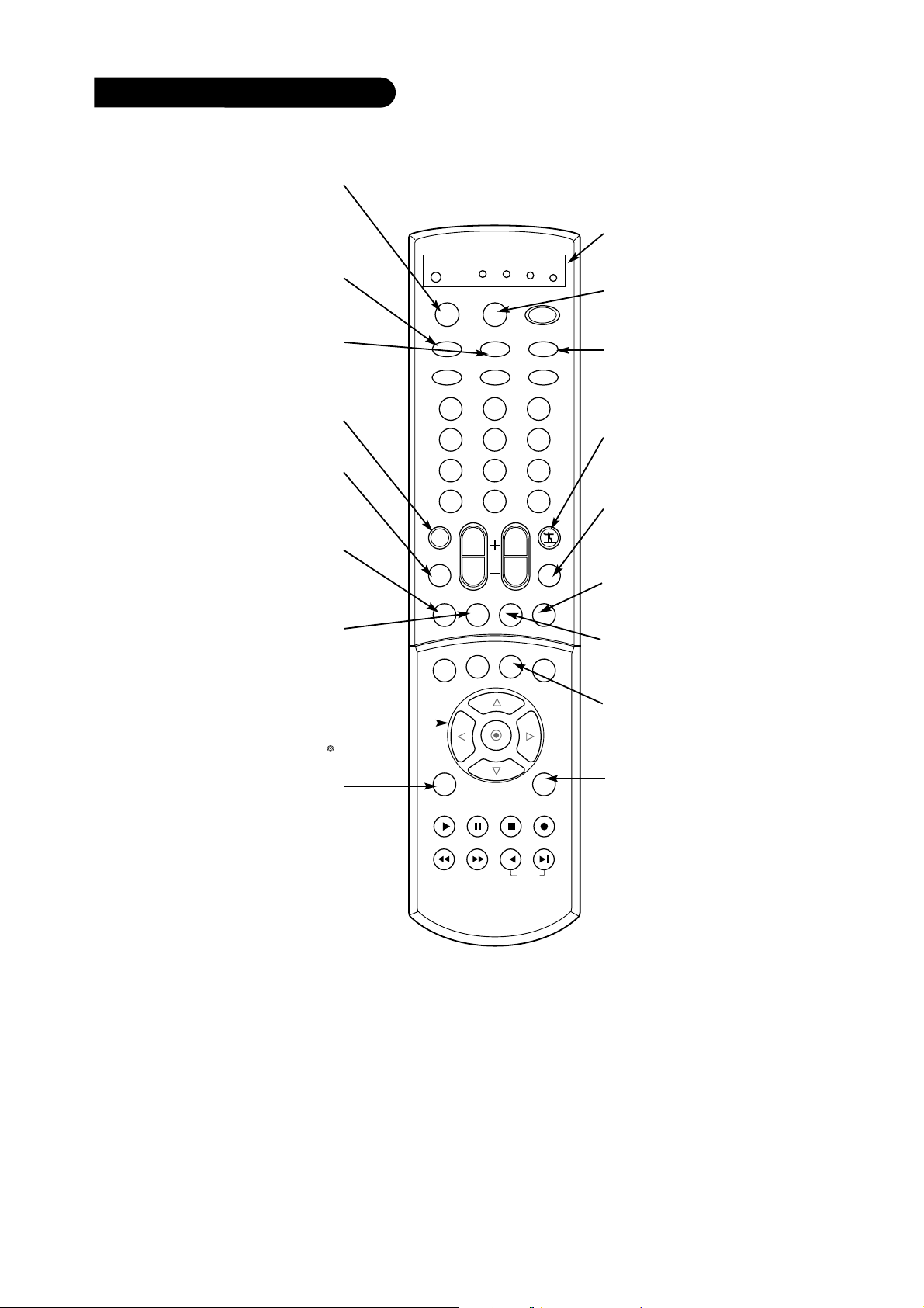
Remote Control Functions in TV Mode
1 2 3
4 5 6
7 8 9
0
tv
mode
light
power
tv/video
dvi
rgb
vcr
cable
dvd
sat
mute
swappipch- pipch+
pip
ratio
recordstop
pause
rew
play
ff
menu exit
cc freeze
pip input
vol
ch
surf
sap
video
comp2comp1
front
skip
enter flashbk
Allows you to navigate the on-screen
menus and to adjust the system set-
tings and preferences, by moving to
an option with
Selects the remote operating
mode: TV, VCR, Cable, DVD
and Satellite. Select other oper-
ating modes, for the remote to
control external devices.
TV/VIDEO
MODE
Selects: Analog, Video1,
Component1-2, RGB, and DVI
Video2, Front video,
input sources.
FRONT
Selects the front video signal if
a device, such as a camcorder
or game player, is connected
to the front video input jack.
MUTE
Switches the sound on or off
SAP
Selects: Mono, Stereo, and
SAP.
PIP
Toggles between PIP, POP
(Picture-out-of-Picture) and
Twin picture mode.
PIPCH-
Changes to next
lower PIP channel
THUMBSTICK
D
F G
and selecting the
E
highlighted option with .
INDICATOR LIGHTS
Show active remote mode
every time any button is
pressed.
LIGHT
Illuminates the remote control keys.
DVI
Selects: DVI-DTV and DVIPC input sources.
SURF
Scrolls the Surf channel list.
VIDEO
Adjusts the factory preset picture according to the room.
SWAP
Swap the signal from your
PIP, POP, twin picture
mode to the main screen.
PIPCH+
Changes to next higher PIP
channel.
FREEZE
Captures and freezes the currentlyviewed sub picture in PIP mode.
Brings up the main
menu to the screen.
MENU
EXIT
Clears all on-screen displays and returns to TV
viewing from any menu.
Page 9
- 9 -
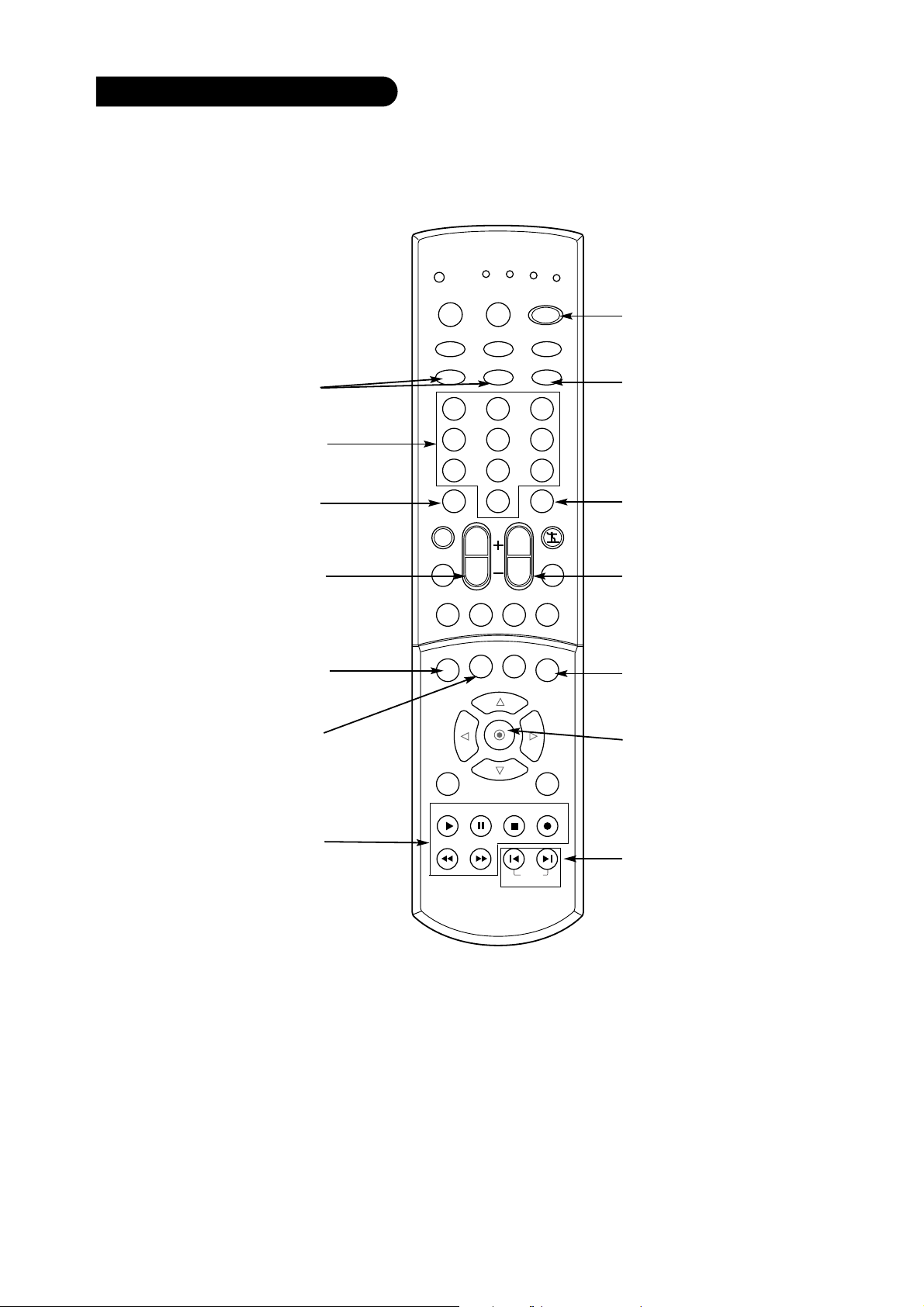
Remote Control Functions in TV Mode
1 2 3
4 5 6
7 8 9
0
tv
mode
light
power
tv/video
dvi
rgb
vcr
cable
dvd
sat
mute
swappipch- pipch+
pip
ratio
recordstop
pause
rew
play
ff
menu exit
cc freeze
pip input
vol
ch
surf
sap
video
comp2comp1
front
skip
enter flashbk
POWER
Turns your TV or any other
programmed equipment on
or off, depending on mode.
Selects component signal sources,
such as DVD or HD receiver.
NUMBER KEYPAD
COMPONENT 1, 2
For direct channel selection and
programming functions.
When in the menu system and
other on-screen displays,
selects highlighted options.
VOLUME UP/DOWN
Increases/decreases the sound
Changes the screen format or
Lets you select a closed caption
mode for displaying captioning
information when provided.
RECORD, PAUSE, REW,
Control the functions on your VCR.
FFWD, PLAY, STOP
ENTER
level.
RATIO
aspect ratio.
CC
RGB
Selects: RGB-DTV and
RGB-PC input sources.
FLASHBK
Tunes to the last channel
viewed.
CHANNEL UP/DOWN
Scrolls through available channels in EZ Scan memory.
PIP INPUT
Selects the input source for the
sub picture.
ENTER
When in the menu system
and other on-screen displays, selects highlighted
options.
SKIP
Playing CDs: Selects
songs.
Playing DVDs: Selects
movie chapters.
Page 10
- 10 -
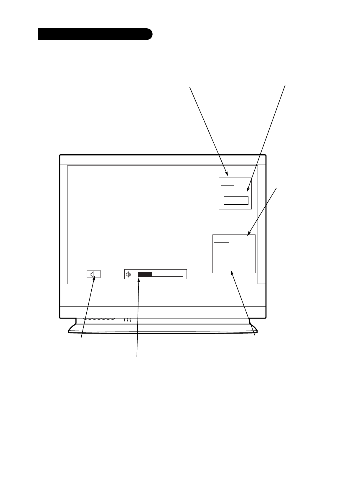
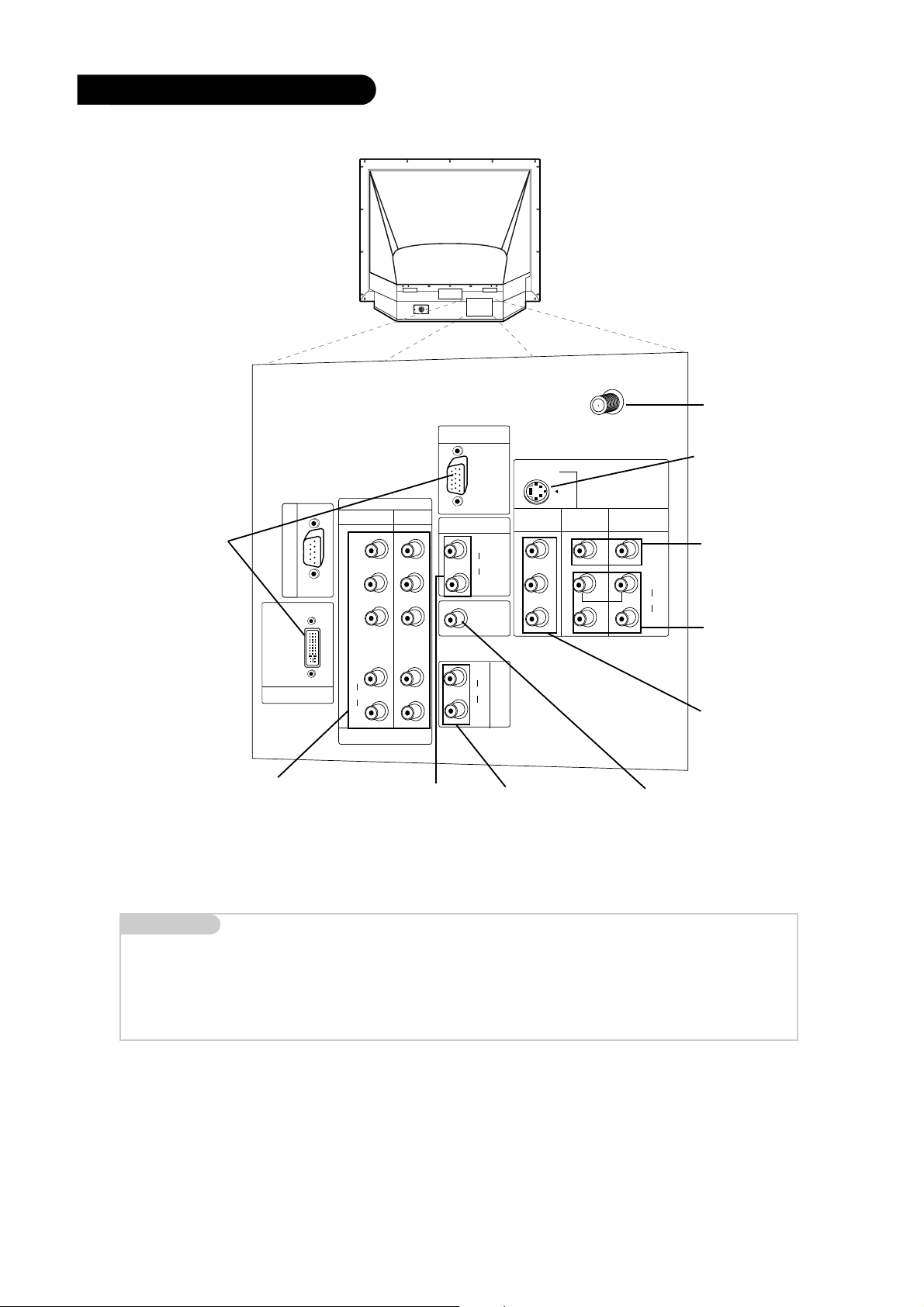
Rear Connections Panel
C
A
L
I
B
R
A
T
I
O
N
PC/DTV
(XGA
/480p
/720p
/1080i)
AUDIO
CENTER
MODE IN
P
R
DVI INPUT
DTV/DVD INPUT
COMPONENT
INPUT2 INPUT1
PB
Y
PC/DTV
(XGA
/480p
/720p
/1080i)
RGB INPUT
RGB/DVI INPUT
(R)
(L)
AUDIO
(R)
(L)
AUDIO
(R)
(L)
AUDIO
V
A
R
I
A
B
L
E
A
U
D
I
O
O
U
T
MONITOR
OUT
VIDEO
INPUT 2
VIDEO
INPUT 1
S-VIDEO
(R)
(L)
AUDIO
VIDEO
MONO
+75 Ω
ANT IN
Connecting cables to your TV.
PC and HD-STB Input
Used to connect from a
PC source or HD-STB
Satellite system.
RF Connector: Antenna
Used to connect analog
cable or antenna signals
to the television, either
directly or through your
cable box.
S-VIDEO In
A connection available with
some high-end equipment
that provides even better
picture quality for Video 2.
Video 1 or 2
Connects the video signals from various types
of equipment.
Left/Right Audio
Used for stereo sound
from various types of
equipment.
Monitor Out
Connects to a second TV
or Monitor.
DVD Component Video and HD Component
Y, Pb, Pr
Video
Some top-of-the-line DVD players use what
is called “component video,” for extremely
accurate picture reproduction. Refer to your
PC and HD-STB Audio
Input
Used for audio connec-
tions from a PC source or
HD-STB Satellite system.
Variable Audio Out
Used to connect either
an external amplifier, or
add a sub-woofer to your
surround sound system.
Audio Center Mode IN
Connect to external Dolby
Digital Center “preamp output.”
DVD manual for further information.
Mini glossary
JACK A connection on the back of a TV, VCR, or any other A/V device. This includes the RF jack and the Audio/Video jacks that are
color-coded.
SIGNAL Picture and sound traveling through cable, or over the air, to your television screen.
Page 11
- 11 -
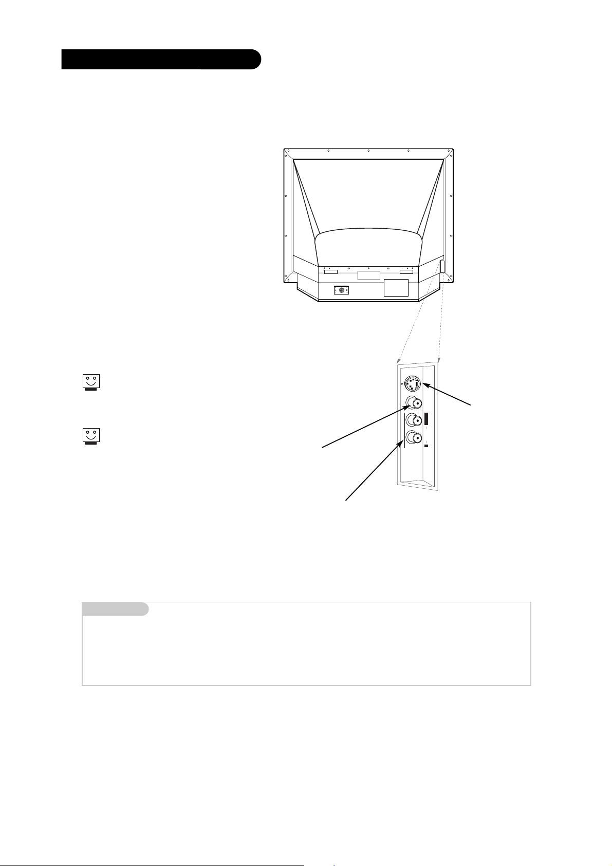
Front Connection Panel
Front A/V Panel
S-VIDEO
VIDEO
FRONT A/V
AUDIO
L/MONOR
There are four jacks on the left front
side behind the screen on your projection TV that make connecting
Audio/Video devices like video games
and camcorders very simple.
The jacks are like those found on the
back jack connection panel. This means
that most equipment that connects to
those types of jacks on the rear jackpack, may be connected to the front
connection panel.
To use the front jacks as the signal
source, select them using Main Source
menu as described on page 22. They
will be named “Front Video” in the Main
Source menu.
When you select Front Video or
Front S-Video, the Front audio
inputs are automatically selected as well.
If you’re connecting a video
game device, make sure to
change the
picture settings with the EZ
Video option in the Video menu.
Video
Connects the video
signals from any
piece of equipment.
Left/Right Audio
Used for stereo
sound from various
types of equipment.
S-Video
A connection available on some very
high-end equipment
that provides better
picture quality than
video input.
Mini glossary
A/V CABLES Audio/Video cables. Three cable connector—Right audio (red), Left audio (white), and Video (yellow). A/V cables are used
A/V DEVICE Any device that produces video or sound (VCR, DVD, cable box, or television).
for stereo playback of videocassettes and for higher quality picture and sound from other A/V devices.
Page 12

- 12 -
SPECIFICATION
Product Specifications
Models
RU-52SZ30 Horizontal Size (inches) 50.4
RU-60SZ30 Horizontal Size (inches) 56.7
Power requirement 120V, 60Hz
Television system American TV Standard, NTSC, ATSC with STB
Television Channel VHF: 2 - 13
Power consumption (W) 250W
Antenna 75 ohm external terminal for VHF/UHF
Audio Output (W) 10W x 2
Supplied accessories Remote control, batteries 2 size AA(Alkaline battery)
Screen Aspect Ratio 16 x 9
LCD Panel Size 0.87 inch (RU-52SZ30), 1.21 inch (RU-60SZ30)
External input ports Video input (3 set)
Height (inches) 38.8
Thickness (inches) 15.3
Weight (lbs) 119
Height (inches) 42.7
Thickness (inches) 19.4
Weight (lbs) 141
UHF: 14 - 69
CATV: 1 - 125
Video output (1 set)
S-Video input (2)
Component input (2 set)
RGB input (1)
DVI input (1)
RGB/DVI audio input (1 set)
Variable audio output (1 set)
Audio center mode input (1)
Calibration port (1)
Design and specifications are subject to change without prior notice.
Page 13

1. Application Object
This instruction is for the application to the LCD projection TV.
2. Notes
(1) The power source insulation of this LCD Projection TV is
not charging type and you may not use the transformer for
insulation. But you better adjust the set after operating it
with insulation transformer between power supply cable and
input part of the set for protecting the adjusting equipment.
(2) The adjustment must be performed under the correct
sequence.
(3) The adjustment must be performed in the circumstance of
25!5°C of temperature and 65!10% of relative humidity if
there is no specific designation.
(4) The input voltage of the receiver must keep 120V, 60Hz in
adjusting.
(5) The set must be operated for 15 minuets preliminarily
before adjustment if there is no specific designation.
The preliminary operation must be performed after receiving 100% white pattern, but reception of the moving picture may also be possible in unavoidable case.
3. Compomation of Adjustment Mode
(1) All adjustment mode are entered by pressing the IN-
START key on the remote control, after adjustment press
the IN-START key to come out.
(2) Compomation of adjustment mode: The first screen com-
position of pressing IN-START key.
(fig. 1) The first screen of adjustment mode
(3) Select menu to adjust(turn to yellow) with using (CH+(D),
CH-(E)) key above screen and press the enter key to
adjust on the wanting menu.
(4) After being inputed for SUB menu, select the SUB menu
with using (CH+(D),CH-(E)) key and adjust the value of
adjustment with using the volume +(F),volume - (G) key.
(5) Press the IN-START key to come out after adjustment,
when (fig.1) is appeared, press again to come out the final
adjustment mode.
(6) SUB menu composition of each adjustment mode
1) Adjust Mode : Sub adjustment menu selected by INSTART key.
RGB alignment is selected in this case.
2) Step123 : Step selection when changing data.
ex) Step123:1 --> Change one by one when changing
data with Volume key
Step123:10 --> Change ten by ten when changing data
with Volume key
You can select 1 by press number key ‘1’, 10 by press
‘12’, 100 by press ‘123’. And you can change data by
1, 10, 100.
3) 10. H_position 315/315/315 : Actual adjusting menu.
4) Micom : V0.50 : Main Micom Version display of Digital
board.
5) SubMicom : V01.31 : Micom Version display of Tuner
board.
6) LCDMicom : V01.31 : Micom Version display of Drive
board.
7) Lamp : 16 : Lamp time display.
4. LCD Adjustment
4-1. NRS Adjustment
[ When the LCD pannel load data on regular pixel using high
speed charge/discharge with sample & holder, the drain
width of TFT gradually decreases and the non-resistance
increases, and comes out regular noise on screen(shows
vertical line by 12 pixel)
This NRS signal is enforced charge/discharge signal so
that the ON/OFF time of TFT mode quickly before starting
active video signal, H/L level adjustment is possible to
each R, G, B.
(1) Required Test Equipments
1) PC Pattern Generator : 16 Step Gray Pattern
2) Fixation Stand
3) Remote Control for Adjustment
4) Circuit thing Jig for Adjustment(Except Driver Board Assy)
(2) Equipment Composition : Follow Fig. 2
(3) Preparation for Adjustment
1) Connect PC Pattern Generator with adjustment Jig like
Fig. 2. (Except Drive part of a circuit block)
2) Select a PC Pattern Generator, 16 Gray.
(4) Adjustment Sequence
1) Turn on a adjustment Jig.
2) Select a RGB_PC by pressing Input Select button on
Remote Control.
3) Enter to adjustment mode by pressing IN-START button on
Remote Control.
EZ ADJUST V*.**
1. VPX3226 Main
2. VPX3226 Sub
3. RGB Alignment
4. 62352
5. Gamma Adjust
6. Uniformity Adj
7. AD9883 Adjust
8. MPX Level Adjust
9. SD-RAM CLK
10. Lamp Replace
Adjust Mode : RGB Alignment Step 123:1
Micom:V0.50 SubMicom:V01.31 LCDMicom:V01.31 Lamp:16
- 13 -
ADJUSTMENT INSTRUCTIONS
10. H_Position 315/315/315
Page 14

4) Select 4. 62352, then ready to adjust 6. RNRSH, 9.
GNRSH and 11. BNRSH.
5) Let’s decrease vertical line Noise by using Volume button.
(Input a R, G, B input signal, then adjust it individually)
6) When finishing the adjustment, get out of adjustment mode
by pressing IN-START button.
4-2. VCOM Adjustment
(1) Required Test Equipments
1) PC PATTERN GENERATOR : Pattern Generator which
can generate each R,G,B signal and can observe the
FLICKER best(ex: me Character Pattern).
2) (Fig. 2) Equipment compositon
3) Remote Control
4) Circuit thing Jig for Adjustment(Except Driver Board Assy
of adjustment model)
(2) Equipment Composition
(3) Preparation for Adjustment
1) Connect the PC Pattern Generator with circuit thing for
adjustment(circuit block except driver part) and adjustment
Jig. shown upper Fig. 2.
2) Set the PC Pattern generator with displayable
format(DTV720p, SVGA 60Hz, XGA 60Hz) and turn on it.
(4) Adjustment Sequence
1) Turn on the adjustment Jig.
2) Select a RGB_PC by pressing Input Select Key on
Remote Control.
3) Enter to adjustment mode by pressing IN-START button on
Remote Control.
4) Select 4. 62352, then ready to adjust 4. 62352 RVCOM, 7.
62352 GVCOM and 10. 62352 BVCOM.
5) Let’s decrease flicker by using Volume button.
(Input a R, G, B input signal, then adjust it individually)
6) When finishing the adjustment, get out of adjustment mode
by pressing IN-START button on Remote Control.
5. Assembling Adjustment
5-1. Screen Tilt & Keystone Adjustment
(1) Required Test Equipments
1) Six angles wrench and spanner for knob adjustment or fixation
2) XGA output PC
3) Remote Control
(2) Preparation for Adjustment
1) Do not assemble the front pannel equipment so that you
can adjust the adjustment knob(Fig. 3).
2) Turn the TV ON and select input mode to RGB_PC.
3) Connect XGA output terminal to PC input of TV.
4) Select window screen.
(3) Adjustment Sequence
1) Stick the Engine(Fig. 3) to the knob poll for adjustment and
check the key stone & tilt watching TV screen.
2) Rotate left/right adjustment knob below and adjust engine
angle.
3) Adjustment adjustment knob of both sides so that the tilt
and keystone are to be under the spec. (The gap between
max and min : under 4mm)
4) After adjusting like 3), fix the engine with screw for fixation
(2EA. adjustment knob and engine fixing screw)
5-2. Screen Position Adjustment
(1) Required Test Equipment
A remote control for adjustment
(2) Preparation for Adjustment
1) Connect a power source with TV Set and turn TV Set on.
2) Do heat run for 15 min and over before adjustment.
3) Receive the main/sub signal of company through 13CH by
split screen.
(3) Horizontal Position Adjustment
1) Press In-START key on the remote control to enter the
adjustment mode.
2) Select 3. RGB Alignment.
- 14 -
(Fig. 2-1) Using Adjustment of Circuit thing for Adjustment
(Fig. 2-2) TV Set status Adjustment
Adjustment Connecctor
Adj.
Jig
Equipment to measure
Optics
(Fig. 3)
Equipment to measure
Optics
SCREEN
Adjustment Jig
SET
Stand
Circuit thing
for Adjustment
PC Pattern
Generator
PC
Page 15

3) Select 10. H_position with channel key in adjust mode.
4) Adjust data with using the left/right key on the remote control in order to be left/right semmetry screen. (Three blocks
of the most outer block must be located the most outer
block.)
(4) Adjustment for Vertical Position
1) Select 16. V_position with channel key in adjust mode.
2) Change the data to symmetrized upper and down of
screen(refer to Fig. 4) and then press the IN-START button on Remote Control to get out of adjustment mode.
5-3. Component2 Offset Adjustment
(1) Required Test Equipment
A remote control for adjustment, 801GF
(2) Preparation for Adjustment
1) Connect a power source with TV Set and turn TV Set on.
2) Do heat run for 15 min and over before adjustment.
3) Receive the Component2.
4) Receive the 720P and HozTVBar Pattern of 801GF.
(3) Offset Adjustment
1) Press IN-START key on the Remote Control to enter the
adjustment mode after more than 10 seconds of receiving
the signals.
2) Press 7. AD9883 adjust to adjust .
3) When the AD9883 Gain Adjust is appeared after AD9883
Offset Adjust, the adjustment is completed.
5-4. Adjustment of White Balance and Gamma
(1) Required Test Equipments
1) Illuminometer (name of model : CA-100) 1EA —>
Measure color of projecting screen center
[ CA-110(name of model) is possible to measure White
Balance and Gamma —- leave it 20Cm from screen
center
Follow a measurement machine manual to set CA-100
and CA-110 measurement machine.
2) Pattern Generator 1EA —> 16 step Gray Pattern, 64 step
Gray Pattern
3) Set Fixation Stand 1EA
4) Remote Control 1EA
5) Circuit thing Jig for adjustment(Except Drive Board Assy of
adjustment model)
--- Programmed Digital Board so that the VDP Test Pattern
can output white signal by 1 level form 0 to 255 level.
(2) A equipment composition
Adjust at the same condition of equipment composition diagram.
(3) Preparation for Adjustment
Compose the equipment follow Fig. 2 and place the set on
the fixation stand.
1) Select the VDP Test Pattern signal to R1, G1, B1.
2) Press the IN-START key to select 4. 62352 and then select
5. RVREF, 8. GVREF, 12. BVREF in adjust mode.
3) Adjust the luminance of CA100 below 0.75Cd. (The adjustment range is 196~202)
4) Exit adjustment mode by pressing IN-START button on
Remote Control.
5) Press the IN-START key on R/C and select 3. 7050 RGB
Set.
6) Check the data 1. RContrast, 8. GContrast, 15. BContrast
is 515. Otherwise set the data 515 by using volume button.
(4) Adjustment Sequence
1) Output the 255,255,255 signal of VDP Test Pattern, then
display the maximum white pattern on screen.
2) Gamma Adjust Mode is display as below when select 5.
Gamma adjust by selecting IN-START key on R/C.
3) Change the 16 Step RGB Data to select white balance
x=283, y=297(D9300K).
4) Measure the luminace with changed data.
5) Set the every Gamma data of 16 step to 2.2 on the basis
of measured luminance data in 3).
(Max luminance *(n1/16)**2.2) — Max luminance : measured luminance data n1 = every step unit when separating signal level to 16 step)
6) Output the 240, 240, 240(15th data in max white output
signal level) in the VDP Test Pattern, change the 15th
RGB Data value to come out white balance x=283,
y=297(D9300K) and measured step luminance in 5).
7) Output the 224, 224, 224(14th data in max white output
signal level) in the VDP Test Pattern, change the 14th
RGB Data value to come out white balance x=283,
y=297(D9300K) and measured step luminance in 5).
- 15 -
(Fig. 4) Adjustment for Horizontal/Vertical Position on Screen
HozTVBar Pattern
* 1st Column : 16 Step Level
* 2nd Column : R Adjustment
Data
* 3rd Column : G Adjustment
Data
* 4th Column : B Adjustment
Data
US13CH
Gamma Adjust Mode
100
100
80
1
234
2
453
3
724
16
RGB 456 Step123
216
411
740
216
387
780
Page 16

8) As shown above, output the VDP Test Pattern signal(208/192/176/160/144/128/112/96/80/64/48/32/16) and
change the RGB Data value of each step to come out
white balance x=283, y=297(D9300K) and measured
lumincance in 3).
(5) Gamma adjustment manually
This is adjustment(after finish the 3-4) to check whether
Gamma/White Balance adjustment are well adjusted and
make correction manually.
1) Prepare the PC Pattern Generator which is possible to output R/G/B of 16 step and 64 step Gray Pattern.
2) Equipment composition : Follow Fig. 2.
3) Turn on the Jig for adjustment.
4) Select the RGB_PC by pressing the input select button on
Remote Control.
5) Output the 16 Gray Pattern in PC Pattern Generator.
Check it with the naked eye whether Screen Gamma and
W/B is right about each Gray.
If it’s not, press the IN-START button on Remote Control
and then adjust the level data of each step manually in
sub menu of 5. Gamma adjust.
6) Output the 64 Gray Pattern in PC Pattern Generator.
Check it with the naked eye whether Screen Gamma and
W/B is right about each Gray or whether there is Gamma
noise.
If there’s any problem, adjust in 5).
7) After finishing adjustment, exit adjustment mode by using
IN-START button on Remote Control.
5-5. White Uniformity Adjustment
(1) Required Test Equipments
1) Uniformity measurement equipment : Equipment which can
measure chromaticity in the whole screen
2) Set Stand 1EA
3) Remote Control for Adjustment
4) Circuit thing Jig for Adjustment(Except Driver Board Assy
of adjustment model)
--- Programmed Digital Board so that the VDP Test Pattern
can output white signal by 1 level form 0 to 255 level.
(2) A equipment composition
Compose the equipment follow Fig. 2 and place the set on
the fixation stand.
(3) Preparation for Adjustment
1) Composite the equipment as shown Fig 2, and place the
set on fixation stand.
2) After inputting company channel 13, adjust color uniformity
like Horizontal/Vertical position adjustment of input signal
part adjustment by using Remote Control for adjustment.
3) After pressing IN-START key on Remote Control for adjustment, select the adjustment mode 6. Uniformity adj.
Refer to register value and correct register value if need.
<Resister Explanation about uniformity adjustment>
1. RamCtrl : s/w saving uniformity write order(Do not adjust)
2. CSHP : Horizontal start point designation ---adjustable
3. CSVP : Vertical start point designation ---adjustable
4. CEHP : Horizontal END point designation ---adjustable
5. CEVP : Vertical END point designation ---adjustable
6. Mode : uniformity mode select --- adjustable if need
*** 0 : 221point & 3level ---- defalut value
*** 1 : 221point & 4level
*** 2 : 825point & 3level
*** 3 : 825point & 4level
7. KHH : Upper 2byte of horizontal line correction coefficient -
- Change according to CSHP, CEHP value.
8. KHL : Upper 2byte of vertical line correction coefficient -Change according to CSHP, CEHP value.
** How to calculate KHH, KHL value
LCD panel size = 1280 x 720
Correction Point = 221 point
--> 17 horizontal points x 13 vertical points
(16 horizontal segments x 12 vertical poins)
O H Coefficient(KHH, KHL)
--> Calculation method (CEHP-CSHP=1280, Horizontal
segment value =16)
9. KVH : Upper 2byte of vertical line correction coefficient -Change according to CSVP, CEVP value.
10. KVL : Upper 2byte of vertical line correction coefficient -Change according to CSVP, CEVP value.
O V Coefficient(KVH, KVL)
--> Calculation method (CEVP-CSVP=720, Vertical seg-
ment value =12)
11. RL1H : Upper 9bit of MID2 brightness correction coefficient in R MIN.
--- Change according to RMIN and RMID2 value.
12. RL1L : Lower 9bit of MID2 brightness correction coefficient in R MIN.
--- Change according to RMIN and RMID2 value.
13. RL2H : Upper 9bit of MID1 brightness correction coefficient in R MID2.
--- Change according to RMID2 and RMID1 value.
14. RL2L : Lower 9bit of MID1 brightness correction coefficient in R MID2.
--- Change according to RMID2 and RMID1 value.
15. RL3H : Upper 9bit of MAX brightness correction coefficient in R MID1.
--- Change according to RMID1 and RMAX value.
(use it while adjusting 4 coefficient)
16. RL3L : Lower 9bit of MAX brightness correction coefficient in R MID1.
--- Change according to RMID1 and RMAX value.
(use it while adjusting 4 coefficient)
- 16 -
H coefficient = 1/(number of pixel intervals between setting in the horizontal
direction)
Hcoeff = 1/((1280/16)-1) = 0.012658227
hex(0.012658227 x 2
16
) = 0 x 033D, Hcoeff(hex) = 0 x 033D + 1 = 0 X 33E
V coefficient = 1/(number of pixel intervals between setting in the horizontal
direction)
Vcoeff = 1/((720/12)-1) = 0.016949152
hex(0.016949152 x 2
16
) = 0 x 0456, Vcoeff(hex) = 0 x 0456 + 1 = 0 X 0457
Page 17

<L Coefficient Calculation Method>
Using 3coefficient Level
Assume that the value of R/G/B MIN, MID2,MID1 is 192, 448,
704.
R/G/B MIN = 192
R/G/B MID2 = 448
R/G/B MID1 = 704
O L Coefficient(RL1H~BL3L)
--> Calculation method (L1)
- calcuate L2, L3 same with L1
17. GL1H : Upper 9bit of MID2 brightness correction coeffi-
cient in G MIN.
--- Change according to GMIN and GMID2 value.
18. GL1L : Lower 9bit of MID2 brightness correction coeffi-
cient in G MIN.
--- Change according to GMIN and GMID2 value.
19. GL2H : Upper 9bit of MID1 brightness correction coeffi-
cient in G MID2.
--- Change according to GMID2 and GMID1 value.
20. GL2L : Lower 9bit of MID1 brightness correction coeffi-
cient in G MID2.
--- Change according to GMID2 and GMID1 value.
21. GL3H : Upper 9bit of MAX brightness correction coeffi-
cient in G MID1.
--- Change according to GMID1 and GMAX value.
(use it while adjusting 4 coefficient)
22. GL3L : Lower 9bit of MAX brightness correction coefficient in G MID1.
--- Change according to GMID1 and GMAX value.
(use it while adjusting 4 coefficient)
23. BL1H : Upper 9bit of MID2 brightness correction coefficient in B MIN.
--- Change according to BMIN and BMID2 value.
24. BL1L : Lower 9bit of MID2 brightness correction coefficient in B MIN.
--- Change according to BMIN and BMID2 value.
25. BL2H : Upper 9bit of MID1 brightness correction coefficient in B MID2.
--- Change according to BMID2 and BMID1 value.
26. BL2L : Lower 9bit of MID1 brightness correction coefficient in B MID2.
--- Change according to BMID2 and BMID1 value.
27. BL3H : Upper 9bit of MAX brightness correction coefficient in B MID1.
--- Change according to BMID1 and BMAX value.
(use it while adjusting 4 coefficient)
28. BL3L : Lower 9bit of MAX brightness correction coefficient
in B MID1.
--- Change according to BMID1 and BMAX value.
(use it while adjusting 4 coefficient)
29. RLMIN : Setting up the MINIUM Level of R --- Set under
200
30. RLMID2 : Setting up the MIDDLE 2nd Level of R --Middle level when 3coefficient
31. RLMID1 : Setting up the MIDDLE 1st Level of R --- Max
level when 3coefficient
32. RLMAX : Setting up the MAX Level of R
33. GLMIN : Setting up the MINIUM Level of G --- Set under
200
34. GLMID2 : Setting up the MIDDLE 2nd Level of G --Middle level when 3coefficient
35. GLMID1 : Setting up the MIDDLE 1st Level of G --- Max
level when 3coefficient
36. GLMAX : Setting up the MAX Level of G
37. BLMIN : Setting up the MINIUM Level of B --- Set under
200
38. BLMID2 : Setting up the MIDDLE 2nd Level of B --Middle level when 3coefficient
39. BLMID1 : Setting up the MIDDLE 1st Level of B --- Max
level when 3coefficient
40. BLMAX : Setting up the MAX Level of B
41. HVSCAN : Setting up the scan direction while adjusting
unifomity - Do not adjust
42. TestMode : uniformity adjustment test - Do not adjust
(4) Adjustment Sequence
1) Adjust the screen coordinates as shown below.
2) Output the VDP TEST PATTERN signal correspond to the
Max value.
Read the white coordinates and communicate 3 line with
ET7050 IC through measurement equipment of optics.
Adjust screen coordinates data to adjust the color uniformity of max point.
At this time, make sure that deviation is +5~-5% and standard is color coordinate of center.
3) Output the VDP TEST PATTERN signal correspond to the
MID value.
Read the white coordinates and communicate 3 line with
ET7050 IC through measurement equipment of optics.
Adjust screen coordinates data to adjust the color uniformity of mid point.
At this time, make sure that deviation is +5~-5% and standard is color coordinate of center.
4) Output the VDP TEST PATTERN signal correspond to the
MIN value.
Read the white coordinate and communicate with ET7050
IC through measurement equipment of optics.
Adjust screen coordinates data to adjust the color uniformity of miner point.
- 17 -
L1 coefficient = 1 / (brightness level(MID2) - brightness level(MIN)
L1coeff = 1 / (448-192) = 1 / 256 = 0.00390625
L1coeff(hex) = hex(0.00390625 x 2
18
) = 0 x 0400
--> L1H(high 9bit) = b’000000010 L1L(low 9bit) = b’000000000
L2 coefficient = 1 / (brightness level(MID1) - brightness level(MID2)
L3 coefficient = 1 / (brightness level(MAX) - brightness level(MID1)
: case of 4 Brightness Level
0 1 2 3 ............xx..........15 16
1
.
yy
.
11
12
(Fig. 5) Screen divisio diagram for uniformity adjustment
Page 18

At this time, make sure that deviation is +5~-5% and standard is color coordinate of center.
5) White the miner, middle, maximum data for each point to
confront to each MICOM address.
5-6. Brightness Adjusment of Main/Sub screen
Operate this adjustment when the brightness of Main/Sub
screen is different.
(1) Receive RF 06Ch. to Main/Sub screen in twin picture.
(2) Let the screen clearly.
(3) Check the “US06CH” with naked eyes in 06Ch. pattern
and if there is difference, adjust like this.
- The field and the letters are distinguished.
(4) Adjusting Main screen
1) Press the “IN Start” key on R/C for adjustment to select
1. VPX3226 main.
2) Adjust to 16. Contrast of adjustment item with +/- key.
(initial value 32)
(5) Adjusting Sub screen
1) Press the “IN Start” key on R/C for adjustment to select
2. VPX3226 sub.
2) Adjust to 16. Contrast of adjustment item with +/- key.
(initial value 32)
* Ask for repairs when the data value is changed over !3.
5-7. Lamp Replace
Use it when the Lamp time is ‘0’.
Press the IN-START key on R/C for adjustment to select
Lamp replace and adjust with volume key.
- 18 -
Page 19

* Connect your dealer or LG service center for replacing of new lamp.
You must replace the lamp when:
Ø The projector image get darker or start to be deteriorated.
Ø The lamp indicator is red(red, flashing alternately).
Ø The massage “LAMP REPLACE“ appears on the screen when turning the projec-
tor lamp on.
* Replace the lamp as below sequence
1. Turn off the projector and unplug the power cable.
(Cool the lamp for more than 1 hour.)
2. Remove the four retaing screws on the lamp cover with a screwdriver of “+“ type
and then lift off the lamp cover.
3. After lifting the lamp cover off, remove the two retaing screw on lamp case with
screwdriver of “-“ type. (refer to fig.2)
4. Lift up the fixed wire handle of the lamp. (refer to fig.3)
5. Pull out the handle slowly and remove the lamp case.
6. Insert the new lamp gently into the correct position. Make sure it is inserted correctly.
7. Tighten the screw you removed in step 3.
8. Replace the lamp cover and tighten the cover screws.(Make sure the almp cover
is securely fastend. If lamp cover is open, the lamp indicator flashes green and
the projector is not turn on.)
* Resetting the lamp time
After pressing the “?“ key on the remote control in Stand-By mode, press the “9876“
and press the “OK“ button.
And then three LED in the front is stop after flashing for a moment.
* Lamp Life Time Confirmation
1. Method1 : Enter ADJ mode with using the remote control. You can be confirmed
because “ Lamp Life Time XX hr“ is appeared.
2. Method2 : With using the remote control offerd to consumer if you press the
menu button continuously, OSD menus will disappear then press the “9876“ and
press the “OK“ button to enter ADJ mode you can see “Lamp Life Time XX hr“
- 19 -
REPLACING THE LAMP
< Fig. 1>
< Fig. 2>
< Fig. 3>
Page 20

Block Diagram
- 20 -
Page 21

- 21 -
Page 22

- 22 -
Page 23

- 23 -
Page 24

EXPLODED VIEW(RU-52SZ30)
- 24 -
430
690
410
420
120
121
300
310
640
650
630
303
307
304
302
305
301
306
123
308
620
670
621
610
611
600
612
124
125
520
550
560
503
502
530
122
174
540
501
680
570
580
401
660
Page 25

- 25 -
EXPLODED VIEW PARTS LIST
120 120-D38E SPEAKER,MID-RANGE LG FOSTER 8 OHM 15/25W 87DB 12
121 6400VG0001B SPEAKER,TWEETER NO FOSTER 8 OHM 20W/30W XX D77
122 3110V00123A CASE,SPEAKER BOX LEFT
123 3550V00159A COVER,SPEAKER BOX LEFT
124 3110V00124A CASE,SPEAKER BOX RIGHT
125 3550V00160A COVER,SPEAKER BOX RIGHT
174 174-225Y POWER CORD ASSEMBLY,6410VUH004A ASSY UL/CSA 3000MM
300 3091V00B46D CABINET ASSEMBLY,RU-52SZ30 NON NB03JA
301 4980V00591A SUPPORTER,SCREEN SBHG ,BOTTOM
302 4980V00592B SUPPORTER,SCREEN SECC RN-52SZ30H
303 3211V00080A FRAME ASSEMBLY,FRONT RN-52SZ10H 3210V00104
304 3211V00081K FRAME ASSEMBLY,FRAME RU-52SZ30 BASE
305 3350V00019B SCREEN,TOPPAN NON RN-52SZ30H 1178*670 SAME 19A PITCH
306 4811V00035B BRACKET ASSEMBLY,SPEAKER RU-52SZ30 NB03JA .
307 4980V00439B SUPPORTER,FRAME ET CENTER FIX RN-52SZ10H
308 3550V00225A COVER,LENS PC+ABS RN-52SZ10H .
310 5020V00654C BUTTON,CONTROL RN-52SZ30H ABS, HF-380 7KEY BUTTON
401 3550V00232B COVER,LAMP RN-52SZ30H PC-ABS .
410 3809V00A39F BACK COVER ASSEMBLY,RU-52SZ30 NON UPPER
420 3809V00A41E BACK COVER ASSEMBLY,RU-52SZ30 NON LOWER
430 5018V00025B MIRROR ASSY,NONE NONE NONE RN-52SZ10H
501 3210V00127A FRAME,RN-52SZ10H CHASSIS DIGITAL
502 3210V00073B FRAME,RU-60SZ10 CHASSIS(SMPS) AB-00EA
503 4811V00021G BRACKET ASSEMBLY,REAR AV RU-52SZ30 NB03JA BRACKET ASSY
520 6871VMMQ05A PCB ASSEMBLY,MAIN PCB ASSEMBLY,MAIN RU-52SZ30 MAIN NB03JA
530 6871VPMA07E PCB ASSEMBLY,POWER SMPS NB03JA RU-52/60SZ30
540 6871VSMV97A PCB ASSEMBLY,SUB TUNER NB03JA RU-52SZ30
550 6871VSMV99A PCB ASSEMBLY,SUB DIGITAL NB03JA RU-52SZ30
560 6871VSMV98A PCB ASSEMBLY,SUB NB03JA RU-52SZ30 COMP
570 6871VPM994H PCB ASSEMBLY,POWER SMPS NB03JA RU-52/60SZ30
580 6871VSMB13F PCB ASSEMBLY,SUB INTER MB03CA BALLAST
600 3141VSNA61D CHASSIS ASSEMBLY,SUB NB03JA BRACK OPTICAL RU-52SZ30
610 3110V00140B CASE ASSY,LAMP RU-60SZ10 PPS+GF40 .
611 6912V00006A LAMP,HIGH PRESSURE MECURY UHP100W 1.3 PHILIPS 100V 1A
612 4930V00230B HOLDER,DUCT BACK FAN PC+ABS RU-52SZ10
620 5900V09002C FAN,DC G9225L12B2-FL DONGYANG 92MM 12V140MA
621 3300V00179C PLATE,DUCT FAN SPCC . RU-60SZ10
622 5900V11001C FAN,DC B1232S12B2 DONGYANG 110MM 12V130MA
630 6871VSN156D PCB ASSEMBLY,MAIN SUB NB03JA PRE-AMP RU-52SZ30
640 6871VSMD03E PCB ASSEMBLY,SUB CONT NB03JA RN-52SZ30H
650 6871VSN194A PCB ASSEMBLY,SUB INTER NB02QA 52 LCD PJTV
660 6871VSN187C PCB ASSEMBLY,SUB LED NB03JA RN-52SZ30H
670 6871VSMU16B PCB ASSEMBLY,SUB NB02QA DRIVER RU-52SZ30
680 6913V00002A BALLAST,EUC-100L/100V PHILIPS FOR LAMP(UHP100W)
690 6871VSN155B PCB ASSEMBLY,SUB NB-02QA SIDE A/V
No. Part No.
Description
Page 26

- 26 -
EXPLODED VIEW(RU-60SZ30)
430
690
410
420
120
121
300
310
640
650
630
303
307
304
302
305
301
306
123
308
620
670
621
610
611
600
612
124
125
520
550
560
503
502
530
122
174
540
501
680
570
580
401
660
Page 27

- 27 -
EXPLODED VIEW PARTS LIST
120 120-D38E SPEAKER,MID-RANGE LG FOSTER 8 OHM 15/25W 87DB 12
121 6400VG0001B SPEAKER,TWEETER NO FOSTER 8 OHM 20W/30W XX D77
122 3110V00123A CASE,SPEAKER BOX LEFT
123 3550V00159A COVER,SPEAKER BOX LEFT
124 3110V00124A CASE,SPEAKER BOX RIGHT
125 3550V00160A COVER,SPEAKER BOX RIGHT
174 174-225Y POWER CORD ASSEMBLY,6410VUH004A ASSY UL/CSA 3000MM
300 3091V00468D CABINET ASSEMBLY,RU-60SZ30 NON NB03JA ,LG
301 4980V00764A SUPPORTER,NON SECC ,TOP FOR SCREEN(4.1T)
302 4980V00765A SUPPORTER,SCREEN SECC ,SIDE FOR SCREEN(4.1T)
303 3211V00047B FRAME ASSEMBLY,FRONT RU-60SZ10 3210V00074B
304 3211V00048J FRAME ASSEMBLY,FRONT LOWER ,RN-60SZ30H
305 3350V00015B SCREEN,TOPPAN NON RN-60SZ30H 1358*776 HARD COATING 2H
306 4811V00032C BRACKET ASSEMBLY,SPEAKER RU-60SZ30 NB03JA ,LG BRAND
307 4980V00359B SUPPORTER,BASE CENTER ET-C(3T) RN-60SZ10H
308 3550V00155B COVER,LENS RN-60SZ10H
310 5020V00654C BUTTON,CONTROL RN-52SZ30H ABS, HF-380 7KEY BUTTON
401 3550V00188C COVER ASSY,RN-60SZ30H PC-ABS ,7227V000056
410 3809V00246H BACK COVER ASSEMBLY,RU-60SZ30 NON ,LG
420 3809V00247E BACK COVER ASSEMBLY,WLP-60M10DW NON .
430 5018V00025C MIRROR ASSY,NONE NONE NONE RT-60SZ10
501 3210V00127A FRAME,RN-52SZ10H CHASSIS DIGITAL . .
502 3210V00073B FRAME,RU-60SZ10 CHASSIS(SMPS) AB-00EA .
503 4811V00034B BRACKET ASSEMBLY,REAR AV RU-60SZ30 NB03JA .
520 6871VMMQ05B PCB ASSEMBLY,MAIN PCB ASSEMBLY,MAIN RU-60SZ30 MAIN NB03JA
530 6871VPMA07E PCB ASSEMBLY,POWER SMPS NB03JA RU-52/60SZ30
540 6871VSMV97B PCB ASSEMBLY,SUB TUNER NB03JA RU-60SZ30
550 6871VSMV99B PCB ASSEMBLY,SUB DIGITAL NB03JA RU-60SZ30
560 6871VSMV98A PCB ASSEMBLY,SUB NB03JA RU-52SZ30 COMP
570 6871VPM994H PCB ASSEMBLY,POWER SMPS NB03JA RU-52/60SZ30
580 6871VSMB13F PCB ASSEMBLY,SUB INTER MB03CA BALLAST
600 3141VSN180F CHASSIS ASSEMBLY,SUB NB03JA BRACK OPTIC RU-60SZ30
610 3110V00140B CASE ASSY,LAMP RU-60SZ10 PPS+GF40
611 6912V00006A LAMP,HIGH PRESSURE MECURY UHP100W 1.3 PHILIPS 100V 1A
612 3110V00205A CASE ASSY,HEAT FLOW RU-60SZ10 . .
620 5900V09002C FAN,DC G9225L12B2-FL DONGYANG 92MM 12V140MA
621 3300V00179C PLATE,DUCT FAN SPCC . RU-60SZ10
622 5900V11001C FAN,DC B1232S12B2 DONGYANG 110MM 12V130MA
630 6871VSN156C PCB ASSEMBLY,SUB NB-02QA PRE-AMP MD 60
640 6871VSMD03D PCB ASSEMBLY,SUB CONT NB03JA RN-60SZ30H
650 6871VSN194A PCB ASSEMBLY,SUB INTER NB02QA 52 LCD PJTV
660 6871VSN187C PCB ASSEMBLY,SUB LED NB03JA RN-52SZ30H
670 6871VSMU16C PCB ASSEMBLY,SUB NB02QA DRIVER RU60SZ30
680 6913V00002A BALLAST,EUC-100L/100V PHILIPS FOR LAMP(UHP100W)
690 6871VSN155B PCB ASSEMBLY,SUB NB-02QA SIDE A/V
No. Part No.
Description
Page 28

REPLACEMENT PARTS LIST
LOCA. NO PART NO DESCRIPTION
IC303
IC304
IC305
IC4
IC400
IC401
IC404
IC405
IC406
IC407
IC407
IC409
IC409
IC410
IC411
IC413
IC5
IC500
IC501
IC503
IC600
IC601
IC601
IC601
IC602
IC603
IC800
IC801B
IC802
IC802B
IC804
IC806
IC807
IC808
IC811
IC820
IC831
IC832
IC841
IC845
T200
Q01
Q02
Q03
Q04
Q05
Q06
0ITI740000Q
0IMMRHY033A
0IMMRHY033A
0IMCRAL006A
0ICTMMI038B
0IMCRTI019A
0ISH052100C
0ISH302122A
0ISH302122A
0ISH302122A
0ISJ156612A
0IKE780500P
0IKE781200P
0ISH052100C
0IKE780800J
0IKE780900M
0IFA754207A
0ILNRMN005A
0ILNRMN005A
0IMCRET002B
0IMCRXL003A
0IFA741230A
0IMCRNS006A
0IMCRMN014A
0IFA754207A
0ISS455880A
0IPH741400E
0ISH817300B
0IKE702700D
0ISH817300B
0ITI740000Q
0IIC271600A
0IMCRSG010A
0IMP242560A
0IMCRON002A
0IMCRSK002A
0ISK615311B
0ISH817300B
0ISH817300B
0ISS781200H
0IZZVF0022B
0TR387500AA
0TR387500AA
0TR387500AA
0TR387500AA
0TR387500AA
0TR387500AA
SN74LVC00AD 14SOP R/TP LOGIC DTV
HY57V643220C(L)T6 86P TSOP TRAY 64M
HY57V643220C(L)T6 86P TSOP TRAY 64M
AT24C16AN10SI2.7 8P SOIC R/TP EEPROM
COPY M306V3FGFP 100P
TFP410 64P TRANSMITTER PANEL
PQ05RD21 4SIP ST REGULATOR
PQ30RV21 TO220
PQ30RV21 TO220
PQ30RV21 TO220
SC15661T2.5TR 3P TO2203L R/TP POWER
KIA78L05BP(AT) 3P 5V,150MA
KIA7812API TO220 ST 3P 12V
PQ05RD21 4SIP ST REGULATOR
KIA7808API 3 ST REGULATOR .
KIA7809API TO220 ST 3P 9V
KA75420ZTA 3P,TO92 TP 4.2V
VPX3226E 44 QFP TRAY VIDEO
VPX3226E 44 QFP TRAY VIDEO
EL2250CS ELANTEC 8P R/TP OP AMP
XC95144XL10TQ100C 3.3V 100P
DM74LS123MX 16SOP
LM4765T 15P TO220 ST AUDIO POWER
MSP3440G QA B8 V3 80 QFP TRAY SOUND
KA75420ZTA 3P,TO92 TP 4.2V
KA4558D 8SOP OP AMP
74HC14D 14SOP TP SHITTER TRIGGER
PC817XF3 4D PHOTO COUPLER
KIA7027AF 3, SOT89 TP RESET IC 2.7V
PC817XF3 4D PHOTO COUPLER
SN74LVC00AD 14SOP R/TP LOGIC DTV
MK2716STR 8P,SOP TP HDTV CLOCK
ST3232CDR SOP16 R/TP RS232
24LC256I/SM 8P,SOP TP 256K
MC33262P 8P DIP ST POWER
STRF6467 5P T0220(LB) ST SWITCHING
STRG6153T(LF1101) 5PIN BK STR
PC817XF3 4D PHOTO COUPLER
PC817XF3 4D PHOTO COUPLER
KA78R12 4P,TO220F BK LOW DROP 12V
AMF730F6M00X2(AF9397) 15P
CHIP 2SC3875S(ALY) KEC
CHIP 2SC3875S(ALY) KEC
CHIP 2SC3875S(ALY) KEC
CHIP 2SC3875S(ALY) KEC
CHIP 2SC3875S(ALY) KEC
CHIP 2SC3875S(ALY) KEC
LOCA. NO PART NO DESCRIPTION
IC01
IC02
IC1
IC100
IC1001
IC1002
IC1004
IC101
IC101
IC102
IC1100
“(52”)
IC1101
IC1102
IC1103
IC1104
IC1105
IC1106
IC1107
IC1200
IC1200
IC1202
IC1202
IC1203
IC1300
IC1301
IC1302
IC1303
IC1304
IC1305
IC1400
IC1401
IC1402
IC1403
IC1404
IC1405
IC1500
IC1501
IC1502
IC1503
IC1504
IC1505
IC1602
IC2
IC200
IC208
IC301
0IMI623200B
0IMI623200B
0IZZVC0051G
0IMCRS5003A
0IPRPFA006A
0IPRPFA007A
0IMMRNE002A
0IPH827150A
0ITK118100B
0IMMRAL014B
0IZZVA0072H
0IZZVA0072G
0IMI623520B
0IAL242561B
0IPRPTI001A
0IKE704200J
0IPRPFA006A
0IPRPFA006A
0IPRPML001B
0IMCRSO008A
0IPRPML001A
0IMO744053B
0IMCRSB010A
0IPRPFA006A
0IMO324000C
0IMCRET001A
0IMCRSB009A
0IMCRSB009A
0IMCRSB008A
0IPRPFA006A
0IMO324000C
0IMCRET001A
0IMCRSB009A
0IMCRSB009A
0IMCRSB008A
0IPRPFA006A
0IMO324000C
0IMCRET001A
0IMCRSB009A
0IMCRSB009A
0IMCRSB008A
0IPRPFA006A
0ISH052100C
0IFA754207A
0IMCRAD002A
0ISO206900A
0ICTMLG003C
M62320FP 16P SOP TP I/O EXPANDER
M62320FP 16P SOP TP I/O EXPANDER
M37272E8A(OTP) DIP 42P BK MICOM
SIL169 CL100 100P LQFP TRAY TMDS
RC1117S33T SOT223 R/TP 3.3VOLT
RC1117S25T SOT223 R/TP 2.5VOLT
UPD64083GF3BA 100 QFP ST 3D YC
P82B715T 8SOP R/TP IIC EXTENDER
TK11840L 8P SOT23L R/TP DCDC
AT24C02N10SI2.7 8P SOIC R/TP 2K
M37272E8A(OTP) DIP 42P DIP DRIVER
M37272E8A(OTP) DIP 42P DIP DRIVER
M62352GP 20P SSOP TP 8BITS 12CH
AT24C256W10SI2.7V 8P
TFP401PZP 100,TQFP R/TP DIGITAL
KIA7042AF SOT89 TP 4.2V
RC1117S33T SOT223 R/TP 3.3VOLT
RC1117S33T SOT223 R/TP 3.3VOLT
MIC29152 5P TO263 R/TP REGULATOR
CXA2151Q 48P QFP TRAY 60LCD
MIC39100 3P SOT223 R/TP LDO TYPE 2.5V
MC74HC4053DW 16SOP 3*2CH.MUX
L3E07050K0A 176QFP TRAY DRIVER IC
RC1117S33T SOT223 R/TP 3.3VOLT
LM324D SO14 TP OP AMP
EL2244CS 8P SO R/TP VIDEO AMPLIFIER
L3E06070D0A 48QFP TRAY DRIVER IC
L3E06070D0A 48QFP TRAY DRIVER IC
L3E01031F0A 48QFP TRAY DRIVE IC
RC1117S33T SOT223 R/TP 3.3VOLT
LM324D SO14 TP OP AMP
EL2244CS 8P SO R/TP VIDEO
L3E06070D0A 48QFP TRAY DRIVER IC
L3E06070D0A 48QFP TRAY DRIVER IC
L3E01031F0A 48QFP TRAY DRIVE IC
RC1117S33T SOT223 R/TP 3.3VOLT
LM324D SO14 TP OP AMP
EL2244CS 8P SO R/TP VIDEO
L3E06070D0A 48QFP TRAY DRIVER IC
L3E06070D0A 48QFP TRAY DRIVER IC
L3E01031F0A 48QFP TRAY DRIVE IC
RC1117S33T SOT223 R/TP 3.3VOLT
PQ05RD21 4SIP ST REGULATOR
KA75420ZTA 3P,TO92 TP 4.2V RESET IC
AD9883A 80P TQFP R/TP DIGITAL
CXA2069Q QFP64 BK I2C BUS AV S/W
LGDT1502M 304P
IC
- 28 -
RUN DATE : 2003.7.4
TRANSISTOR
Page 29

- 29 -
LOCA. NO PART NO DESCRIPTION
Q1
Q100
Q1001
Q1002
Q1003
Q1004
Q1005
Q1006
Q1007
Q1008
Q1009
Q101
Q1010
Q1011
Q1012
Q1013
Q1014
Q1015
Q1016
Q1017
Q102
Q103
Q107
Q109
Q1200
Q1201
Q1202
Q1203
Q1204
Q1205
Q1206
Q1207
Q1208
Q1209
Q1210
Q1213
Q1214
Q1215
Q1216
Q1217
Q1218
Q1219
Q2
Q201
Q202
Q203
Q204
Q205
Q206
Q207
Q208
Q209
0TR387500AA
0TR830009BA
0TR387500AA
0TR387500AA
0TR387500AA
0TR150400BA
0TR150400BA
0TR387500AA
0TR150400BA
0TR150400BA
0TR387500AA
0TR830009BA
0TR150400BA
0TR150400BA
0TR150400BA
0TR150400BA
0TR387500AA
0TR150400BA
0TR387500AA
0TR150400BA
0TRKE80038A
0TR387500AA
0TR387500AA
0TR387500AA
0TR387500AA
0TR387500AA
0TR387500AA
0TR387500AA
0TR387500AA
0TR387500AA
0TR387500AA
0TR387500AA
0TR387500AA
0TR150400BA
0TR102009AG
0TR387500AA
0TR387500AA
0TR150400BA
0TR150400BA
0TR387500AA
0TR387500AA
0TR387500AA
0TR150400BA
0TR387500AA
0TR387500AA
0TR387500AA
0TR387500AA
0TR387500AA
0TR387500AA
0TR387500AA
0TR387500AA
0TR387500AA
CHIP 2SC3875S(ALY) KEC
BSS83
CHIP 2SC3875S(ALY) KEC
CHIP 2SC3875S(ALY) KEC
CHIP 2SC3875S(ALY) KEC
CHIP 2SA1504S(ASY) KEC
CHIP 2SA1504S(ASY) KEC
CHIP 2SC3875S(ALY) KEC
CHIP 2SA1504S(ASY) KEC
CHIP 2SA1504S(ASY) KEC
CHIP 2SC3875S(ALY) KEC
BSS83
CHIP 2SA1504S(ASY) KEC
CHIP 2SA1504S(ASY) KEC
CHIP 2SA1504S(ASY) KEC
CHIP 2SA1504S(ASY) KEC
CHIP 2SC3875S(ALY) KEC
CHIP 2SA1504S(ASY) KEC
CHIP 2SC3875S(ALY) KEC
CHIP 2SA1504S(ASY) KEC
KTC3552TRTK SOT23F 50V 3A
CHIP 2SC3875S(ALY) KEC
CHIP 2SC3875S(ALY) KEC
CHIP 2SC3875S(ALY) KEC
CHIP 2SC3875S(ALY) KEC
CHIP 2SC3875S(ALY) KEC
CHIP 2SC3875S(ALY) KEC
CHIP 2SC3875S(ALY) KEC
CHIP 2SC3875S(ALY) KEC
CHIP 2SC3875S(ALY) KEC
CHIP 2SC3875S(ALY) KEC
CHIP 2SC3875S(ALY) KEC
CHIP 2SC3875S(ALY) KEC
CHIP 2SA1504S(ASY) KEC
CHIP KRC102S
CHIP 2SC3875S(ALY) KEC
CHIP 2SC3875S(ALY) KEC
CHIP 2SA1504S(ASY) KEC
CHIP 2SA1504S(ASY) KEC
CHIP 2SC3875S(ALY) KEC
CHIP 2SC3875S(ALY) KEC
CHIP 2SC3875S(ALY) KEC
CHIP 2SA1504S(ASY) KEC
CHIP 2SC3875S(ALY) KEC
CHIP 2SC3875S(ALY) KEC
CHIP 2SC3875S(ALY) KEC
CHIP 2SC3875S(ALY) KEC
CHIP 2SC3875S(ALY) KEC
CHIP 2SC3875S(ALY) KEC
CHIP 2SC3875S(ALY) KEC
CHIP 2SC3875S(ALY) KEC
CHIP 2SC3875S(ALY) KEC
LOCA. NO PART NO DESCRIPTION
Q210
Q211
Q500
Q501
Q502
Q504
Q601
Q601
Q602
Q602
Q603
Q605
Q605
Q810
Q841
Q842
Q851
D01
D02
D03
D1
D100
D101
D2
D3
D300
D404
D430
D431
D432
D433
D435
D436
D437
D438
D439
D5
D601
D603
D605
D606
D607
D801
D801
D802
D803
D804
D805
D806
D810
0TR387500AA
0TR387500AA
0TR150400BA
0TR830009BA
0TR830009BA
0TR102009AG
0TR387500AA
0TR387500AA
0TR387500AA
0TR387500AA
0TR322709AA
0TR387500AA
0TR150400BA
0TF283700AA
0TR945009AA
0TR322709AA
0TR945009AA
0DL200000CA
0DL200000CA
0DL200000CA
0DD184009AA
0DD184009AA
0DD184009AA
0DD184009AA
0DD226239AA
0DL233309AC
0DD184009AA
0DS113379BA
0DS113379BA
0DS113379BA
0DS113379BA
0DS113379BA
0DS113379BA
0DS113379BA
0DS113379BA
0DS113379BA
0DD184009AA
0DD184009AA
0DD184009AA
0DD184009AA
0DD184009AA
0DD184009AA
0DR050008AA
0DD606000AA
0DR050008AA
0DR050008AA
0DR050008AA
0DRSE00038A
0DRSE00038A
0DD100009AM
CHIP 2SC3875S(ALY) KEC
CHIP 2SC3875S(ALY) KEC
CHIP 2SA1504S(ASY) KEC
BSS83
BSS83
CHIP KRC102S
CHIP 2SC3875S(ALY) KEC
CHIP 2SC3875S(ALY) KEC
CHIP 2SC3875S(ALY) KEC
CHIP 2SC3875S(ALY) KEC
KTC3227Y,TP(KTC1627A),KEC
CHIP 2SC3875S(ALY) KEC
CHIP 2SA1504S(ASY) KEC
2SK2837 500V 20A TO3P
KSC945CY TO92 50V 150MA
KTC3227Y,TP(KTC1627A),KEC
KSC945CY TO92 50V 150MA
LED,SAM5670(DL2LRG) BK YGREEN
LED,SAM5670(DL2LRG) BK YGREEN
LED,SAM5670(DL2LRG) BK YGREEN
KDS184S CHIP 85V 300MA KEC TP
KDS184S CHIP 85V 300MA KEC TP
KDS184S CHIP 85V 300MA KEC TP
KDS184S CHIP 85V 300MA KEC TP
CHIP KDS226 SOT23
LED,SAM2333
KDS184S CHIP 85V 300MA KEC TP
1SS133 T72 DO34 90V
1SS133 T72 DO34 90V
1SS133 T72 DO34 90V
1SS133 T72 DO34 90V
1SS133 T72 DO34 90V
1SS133 T72 DO34 90V
1SS133 T72 DO34 90V
1SS133 T72 DO34 90V
1SS133 T72 DO34 90V
KDS184S CHIP 85V 300MA KEC TP
KDS184S CHIP 85V 300MA KEC TP
KDS184S CHIP 85V 300MA KEC TP
KDS184S CHIP 85V 300MA KEC TP
KDS184S CHIP 85V 300MA KEC TP
KDS184S CHIP 85V 300MA KEC TP
SD05.TC SOD323 5V 5A 15A
RBV606 600V 6A 150A NA 10UA
SD05.TC SOD323 5V 5A 15A
SD05.TC SOD323 5V 5A 15A
SD05.TC SOD323 5V 5A 15A
SDC15 SOT23 12.8V 10A .A .SEC 100NA
SDC15 SOT23 12.8V 10A .A .SEC 100NA
EU1ZV(1) TP SANKEN
DIODE
Page 30

- 30 -
LOCA. NO PART NO DESCRIPTION
D820
D821
D822
D832
D833
D834
D841
D845
D881
D881
Q810
ZD01
ZD1
ZD1
ZD10
ZD11
ZD12
ZD2
ZD2
ZD201
ZD202
ZD203
ZD204
ZD3
ZD3
ZD4
ZD5
ZD6
ZD601
ZD602
ZD8
ZD841
ZD851
ZD9
C01
C07
C1
C100
C101
C1011
C1013
C1019
C1020
C1023
C103
C1035
C1036
C1039
C1042
C1049
0DD100009AM
0DD100009AM
0DD100009AM
0DR010009AA
0DD100009AM
0DD260000BB
0DD100009AP
0DD414809ED
0DD120000BB
0DD420000BB
0DR260001AA
0DR050008AA
0DR050008AA
0DZ620009BB
0DZ620009BB
0DR050008AA
0DR050008AA
0DR050008AA
0DZ620009BB
0DZ560009CF
0DZ560009CF
0DZ560009CF
0DZ560009CF
0DR050008AA
0DZ620009BB
0DZ620009BB
0DZ620009BB
0DZ620009BB
0DZ560009CF
0DZ560009CF
0DR050008AA
0DZ620009BB
0DZ620009BB
0DZ620009BB
0CE226VF6DC
0CE476VF6DC
0CE476DF618
0CE226SF6DC
0CE106VF6DC
0CE476VF6DC
0CE476VF6DC
0CE105VK6DC
0CE476VF6DC
0CE476VF6DC
0CE475VK6DC
0CE106VF6DC
0CE106VF6DC
0CE476VF6DC
0CE106VF6DC
0CE106VF6DC
EU1ZV(1) TP SANKEN
EU1ZV(1) TP SANKEN
EU1ZV(1) TP SANKEN
EG01C 1000V 0.5A 10A 100NSEC 50UA
EU1ZV(1) TP SANKEN
BRIDGE D2SBA60(STK) SHINDENKEN
EG1ZV(1) TP SANKEN TP SANKEN
1N4148 TP GRANDE
FMLG12S
D4L20U SHINDENGEN
FMG26S TO220 600V 6A 50A
SD05.TC SOD323 5V 5A 15A
SD05.TC SOD323 5V 5A 15A
ZENERS,MTZJ6.2B
ZENERS,MTZJ6.2B
SD05.TC SOD323 5V 5A 15A
SD05.TC SOD323 5V 5A 15A
SD05.TC SOD323 5V 5A 15A
ZENERS,MTZJ6.2B
ZENERS,MTZJ5.6B
ZENERS,MTZJ5.6B
ZENERS,MTZJ5.6B
ZENERS,MTZJ5.6B
SD05.TC SOD323 5V 5A 15A
ZENERS,MTZJ6.2B
ZENERS,MTZJ6.2B
ZENERS,MTZJ6.2B
ZENERS,MTZJ6.2B
ZENERS,MTZJ5.6B
ZENERS,MTZJ5.6B
SD05.TC SOD323 5V 5A 15A
ZENERS,MTZJ6.2B
ZENERS,MTZJ6.2B
ZENERS,MTZJ6.2B
22UF MV 16V 20%
47UF MV 16V 20%
47UF STD 16V M
22UF MVG 16V M
10UF MV 16V 20%
47UF MV 16V 20%
47UF MV 16V 20%
1UF MV 50V 20%
47UF MV 16V 20%
47UF MV 16V 20%
4.7UF MV 50V 20%
10UF MV 16V 20%
10UF MV 16V 20%
47UF MV 16V 20%
10UF MV 16V 20%
10UF MV 16V 20%
LOCA. NO PART NO DESCRIPTION
C105
C1055
C106
C1060
C108
C11
C110
C1100
C1101
C1102
C1103
C1104
C1105
C1106
C1107
C1108
C111
C1110
C1111
C1112
C1114
C1116
C1118
C112
C112
C1122
C1125
C1133
C1134
C1138
C1139
C1143
C117
C1200
C1201
C1202
C1202
C1204
C1205
C1206
C1207
C1208
C1209
C1216
C1217
C1218
C1226
C1234
C1237
C124
C1250
C1251
0CE476VF6DC
0CE106VF6DC
0CE476VK6DC
0CE476SF6DC
0CE106VF6DC
0CE226VF6DC
0CE476VK6DC
0CK103CK56A
0CE476VH6DC
0CK103CK56A
0CK103CK56A
0CE105VK6DC
0CC180CKH1A
0CC180CKH1A
0CK103CK56A
0CE476VH6DC
0CE476VF6DC
0CE476VH6DC
0CK103CK56A
0CE476VH6DC
0CE107VH6DC
0CE107SF6DC
0CE107SF6DC
0CE106SF6DC
0CE475VK6DC
0CE476VH6DC
0CE476VH6DC
0CE476VH6DC
0CE476VH6DC
0CE476VH6DC
0CE476VH6DC
0CE476VH6DC
0CQ2231N509
0CE476VH6DC
0CE106VF6DC
0CE106VF6DC
0CE107SF6DC
0CE106VF6DC
0CE106VF6DC
0CE106VF6DC
0CE106VF6DC
0CE106VF6DC
0CE106VF6DC
0CE106VF6DC
0CE106VF6DC
0CE106VF6DC
0CE476VH6DC
0CE476VF6DC
0CE105VK6DC
0CQ2231N509
0CE105VK6DC
0CE105VK6DC
47UF MV 16V 20%
10UF MV 16V 20%
47UF MV 50V 20%
47UF MVG 16V M
10UF MV 16V 20%
22UF MV 16V 20%
47UF MV 50V 20%
0.01UF 1608 50V 10%
47UF MV 25V 20%
0.01UF 1608 50V 10%
0.01UF 1608 50V 10%
1UF MV 50V 20%
18PF 1608 50V 2%
18PF 1608 50V 2%
0.01UF 1608 50V 10%
47UF MV 25V 20%
47UF MV 16V 20%
47UF MV 25V 20%
0.01UF 1608 50V 10%
47UF MV 25V 20%
100UF MV 25V 20%
100UF MVG 16V M
100UF MVG 16V M
10UF MVG 16V 20%
4.7UF MV 50V 20%
47UF MV 25V 20%
47UF MV 25V 20%
47UF MV 25V 20%
47UF MV 25V 20%
47UF MV 25V 20%
47UF MV 25V 20%
47UF MV 25V 20%
0.022U 100V K
47UF MV 25V 20%
10UF MV 16V 20%
10UF MV 16V 20%
100UF MVG 16V M
10UF MV 16V 20%
10UF MV 16V 20%
10UF MV 16V 20%
10UF MV 16V 20%
10UF MV 16V 20%
10UF MV 16V 20%
10UF MV 16V 20%
10UF MV 16V 20%
10UF MV 16V 20%
47UF MV 25V 20%
47UF MV 16V 20%
1UF MV 50V 20%
0.022U 100V K
1UF MV 50V 20%
1UF MV 50V 20%
CAPACITOR
Page 31

- 31 -
LOCA. NO PART NO DESCRIPTION
C126
C128
C129
C1301
C1305
C1308
C1309
C131
C1310
C1311
C1313
C1319
C1320
C1321
C1322
C1324
C1325
C133
C1330
C1335
C1336
C1340
C1341
C140
C140
C1401
C1405
C1408
C1409
C1410
C1411
C1413
C1419
C1420
C1421
C1422
C1424
C1425
C1429
C1435
C1436
C144
C1441
C146
C149
C15
C1501
C1505
C1508
C1509
C1510
C1511
0CE226SF6DC
0CE476VK6DC
0CE226SF6DC
0CE476VH6DC
0CK103CK56A
0CE476VH6DC
0CE476VH6DC
0CE476VK6DC
0CK103CK56A
0CK103CK56A
0CK103CK56A
0CE476VH6DC
0CE476VH6DC
0CK103CK56A
0CK103CK56A
0CE476VH6DC
0CE476VH6DC
0CE476VH6DC
0CE476VH6DC
0CE476VH6DC
0CE476VH6DC
0CK103CK56A
0CE476VH6DC
0CE226SF6DC
0CE475VK6DC
0CE476VH6DC
0CK103CK56A
0CE476VH6DC
0CE476VH6DC
0CK103CK56A
0CK103CK56A
0CK103CK56A
0CE476VH6DC
0CE476VH6DC
0CK103CK56A
0CK103CK56A
0CE476VH6DC
0CE476VH6DC
0CE476VH6DC
0CE476VH6DC
0CE476VH6DC
0CE226SF6DC
0CE476VH6DC
0CE106SF6DC
0CE106SF6DC
0CE105VK6DC
0CE476VH6DC
0CK103CK56A
0CE476VH6DC
0CE476VH6DC
0CK103CK56A
0CK103CK56A
22UF MVG 16V M
47UF MV 50V 20%
22UF MVG 16V M
47UF MV 25V 20%
0.01UF 1608 50V 10%
47UF MV 25V 20%
47UF MV 25V 20%
47UF MV 50V 20%
0.01UF 1608 50V 10%
0.01UF 1608 50V 10%
0.01UF 1608 50V 10%
47UF MV 25V 20%
47UF MV 25V 20%
0.01UF 1608 50V 10%
0.01UF 1608 50V 10%
47UF MV 25V 20%
47UF MV 25V 20%
47UF MV 25V 20%
47UF MV 25V 20%
47UF MV 25V 20%
47UF MV 25V 20%
0.01UF 1608 50V 10%
47UF MV 25V 20%
22UF MVG 16V M
4.7UF MV 50V 20%
47UF MV 25V 20%
0.01UF 1608 50V 10%
47UF MV 25V 20%
47UF MV 25V 20%
0.01UF 1608 50V 10%
0.01UF 1608 50V 10%
0.01UF 1608 50V 10%
47UF MV 25V 20%
47UF MV 25V 20%
0.01UF 1608 50V 10%
0.01UF 1608 50V 10%
47UF MV 25V 20%
47UF MV 25V 20%
47UF MV 25V 20%
47UF MV 25V 20%
47UF MV 25V 20%
22UF MVG 16V M
47UF MV 25V 20%
10UF MVG 16V 20%
10UF MVG 16V 20%
1UF MV 50V 20%
47UF MV 25V 20%
0.01UF 1608 50V 10%
47UF MV 25V 20%
47UF MV 25V 20%
0.01UF 1608 50V 10%
0.01UF 1608 50V 10%
LOCA. NO PART NO DESCRIPTION
C1513
C1519
C152
C1520
C1521
C1522
C1524
C1525
C1529
C1535
C1536
C1541
C16
C1620
C1621
C2
C20
C200
C202
C204
C205
C205
C206
C209
C212
C216
C218
C222
C223
C227
C228
C231
C245
C246
C247
C247
C248
C250
C252
C260
C261
C262
C29
C3
C31
C312
C314
C406
C406
C407
C408
C409
0CK103CK56A
0CE476VH6DC
0CE106SF6DC
0CE476VH6DC
0CK103CK56A
0CK103CK56A
0CE476VH6DC
0CE476VH6DC
0CE476VH6DC
0CE476VH6DC
0CE476VH6DC
0CE476VH6DC
0CE476VF6DC
0CE107VF6DC
0CE107VF6DC
0CN1030F679
0CE105VK6DC
0CE226SF6DC
0CE106SF6DC
0CE105VK6DC
0CE106SF6DC
0CE105VK6DC
0CE106SF6DC
0CE105VK6DC
0CE105VK6DC
0CE105VK6DC
0CE105VK6DC
0CE105VK6DC
0CE105VK6DC
0CE226VF6DC
0CK823DK56A
0CE107SF6DC
0CE106SF6DC
0CE226SF6DC
0CE106SF6DC
0CE227VF6DC
0CE226SF6DC
0CE106SF6DC
0CE226SF6DC
0CE475VK6DC
0CE475VK6DC
0CE227VF6DC
0CE105VK6DC
0CE476VF6DC
0CE226VF6DC
0CE226SF6DC
0CE226SF6DC
0CE226SF6DC
0CE227VF6DC
0CE107VH6DC
0CE107SF6DC
0CE107SF6DC
0.01UF 1608 50V 10%
47UF MV 25V 20%
10UF MVG 16V 20%
47UF MV 25V 20%
0.01UF 1608 50V 10%
0.01UF 1608 50V 10%
47UF MV 25V 20%
47UF MV 25V 20%
47UF MV 25V 20%
47UF MV 25V 20%
47UF MV 25V 20%
47UF MV 25V 20%
47UF MV 16V 20%
100UF MV 16V 20%
100UF MV 16V 20%
10000P 16V M
1UF MV 50V 20%
22UF MVG 16V M
10UF MVG 16V 20%
1UF MV 50V 20%
10UF MVG 16V 20%
1UF MV 50V 20%
10UF MVG 16V 20%
1UF MV 50V 20%
1UF MV 50V 20%
1UF MV 50V 20%
1UF MV 50V 20%
1UF MV 50V 20%
1UF MV 50V 20%
22UF MV 16V 20%
82000PF 2012 50V 10%
100UF MVG 16V M
10UF MVG 16V 20%
22UF MVG 16V M
10UF MVG 16V 20%
220UF MV 16V 20%
22UF MVG 16V M
10UF MVG 16V 20%
22UF MVG 16V M
4.7UF MV 50V 20%
4.7UF MV 50V 20%
220UF MV 16V 20%
1UF MV 50V 20%
47UF MV 16V 20%
22UF MV 16V 20%
22UF MVG 16V M
22UF MVG 16V M
22UF MVG 16V M
220UF MV 16V 20%
100UF MV 25V 20%
100UF MVG 16V M
100UF MVG 16V M
For Capacitor & Resistors, the
charactors at 2nd and 3rd digit
in the P/No. means as follows;
CC, CX, CK, CN : Ceramic
CQ : Polyestor
CE : Electrolytic
RD : Carbon Film
RS : Metal Oxide Film
RN : Metal Film
RF : Fusible
Page 32

- 32 -
LOCA. NO PART NO DESCRIPTION
C410
C411
C412
C427
C428
C434
C435
C437
C438
C451
C453
C454
C456
C456
C462
C480
C482
C50
C500
C501
C503
C505
C518
C519
C522
C525
C541
C600
C601
C602
C603
C604
C606
C611
C612
C616
C616
C617
C619
C621
C622
C623
C624
C627
C628
C628
C629
C630
C631
C631
C632
C633
0CE107SF6DC
0CE107SF6DC
0CE476VF6DC
0CE227DD618
0CE227DD618
0CE227DD618
0CE227DD618
0CE227DD618
0CE107DH618
0CE107DD618
0CE107DD618
0CE336SC6DC
0CK105DF64A
0CE107VH6DC
0CE227DF618
0CE227DH618
0CE107DF618
0CE227SC6DC
0CE106SF6DC
0CE226SF6DC
0CE106SF6DC
0CE226SF6DC
0CE106SF6DC
0CE226SF6DC
0CE106SF6DC
0CE226SF6DC
0CK105DF64A
0CE226SF6DC
0CQ1831N509
0CQ1831N509
0CE106DK618
0CE106DK618
0CE107SF6DC
0CE106DK618
0CE226DK618
0CE107SF6DC
0CE475DK618
181-442Z
0CE335VK6DC
0CE106VF6DC
0CE106VF6DC
0CE108DF618
0CE106DF618
0CE108DK61A
0CE106VF6DC
181-442Z
0CE104DK618
0CE106VF6DC
0CE107SF6DC
0CE108DJ618
181-442Z
0CE108DJ618
100UF MVG 16V M
100UF MVG 16V M
47UF MV 16V 20%
220UF STD 10V M
220UF STD 10V M
220UF STD 10V M
220UF STD 10V M
220UF STD 10V M
100UF STD 25V M
100UF STD 10V M
100UF STD 10V M
33UF MVG 6.3V M
1UF 2012 16V 20%
100UF MV 25V 20%
220UF STD 16V M
220UF STD 25V M
100UF STD 16V M
220UF MVG 6.3V M
10UF MVG 16V 20%
22UF MVG 16V M
10UF MVG 16V 20%
22UF MVG 16V M
10UF MVG 16V 20%
22UF MVG 16V M
10UF MVG 16V 20%
22UF MVG 16V M
1UF 2012 16V 20%
22UF MVG 16V M
0.018U 100V K
0.018U 100V K
10UF STD 50V M
10UF STD 50V M
100UF MVG 16V M
10UF STD 50V M
22UF STD 50V M
100UF MVG 16V M
4.7UF STD 50V 20%
PE,ECQB1H104KF3(TR)
3.3UF MV 50V 20%
10UF MV 16V 20%
10UF MV 16V 20%
1000UF STD 16V M
10UF STD 16V M
1000UF STD 50V M
10UF MV 16V 20%
PE,ECQB1H104KF3(TR)
0.1000UF STD 50V M
10UF MV 16V 20%
100UF MVG 16V M
1000UF STD 35V M
PE,ECQB1H104KF3(TR)
1000UF STD 35V M
LOCA. NO PART NO DESCRIPTION
C634
C643
C643
C644
C645
C648
C664
C668
C669
C800
C801
C801
C801B
C802
C804
C804
C805
C806
C806
C807
C807
C808
C809
C814
C814
C818
C818
C820
C821
C822
C823
C824
C825
C829
C831
C832
C832
C833
C835
C836
C837
C841
C843
C845
C853
C855
C856
C858
C859
C862
C865
C873
181-442Z
0CE476VF6DC
0CE226DK618
181-442Z
181-442Z
0CE335VK6DC
0CE335VK6DC
0CE105VK6DC
0CE105VK6DC
0CE106SF6DC
0CK105DF64A
0CQZVBK002B
0CE106BK618
0CQZVBK002A
0CE106SF6DC
0CF1050W470
0CK10202510
0CE226SF6DC
0CK10202510
0CE336SC6DC
0CK1020K515
0CQ1021N519
181-007J
0CE106SF6DC
0CE107BK618
0CE226SF6DC
181-091R
181-001K
181-014Y
0CK1020K515
0CK1020K515
0CE107BK618
0CE336BK618
181-120L
181-035N
0CQ1021N519
0CQ1021N509
0CE107BH618
181-010K
0CE476EU61A
0CK1040K945
0CE108BF618
0CK1040K945
0CE107BF618
0CE108BF618
0CE228BF618
0CK1040K945
0CE477DF618
181-091Q
0CE228BF618
181-091Q
0CE108BK61A
PE,ECQB1H104KF3(TR)
47UF MV 16V 20%
22UF STD 50V M
PE,ECQB1H104KF3(TR)
PE,ECQB1H104KF3(TR)
3.3UF MV 50V 20%
3.3UF MV 50V 20%
1UF MV 50V 20%
1UF MV 50V 20%
10UF MVG 16V 20%
1UF 2012 16V 20%
A.C 275V 0.15UF K (S=22.5)
10UF KME 50V M
A.C 275V 0.1UF M (S=15)
10UF MVG 16V 20%
1UF 0 500V 5%
1000P 2KV K B S
22UF MVG 16V M
1000P 2KV K B S
33UF MVG 6.3V M
1000P 50V K B TS
0.001U 100V K
MPE ECQV1H564JL3(TR), 50V 0.56UF J
10UF MVG 16V 20%
100UF KME 50V M
22UF MVG 16V M
R 1000PF 1KV 10%,10%
CE 450V 220UF M LUG(105)
MPP 1.6KV 0.0015UF J
1000P 50V K B TS
1000P 50V K B TS
100UF KME 50V M
33UF KME TYPE 50V 20%
3300PF 4KV M E FMTW LEAD4.5
DE1010 B KD 471M
0.001U 100V K
0.001U 100V K
100UF KME 25V M
PP 0.01UF 630V 5%
47UF KMG 400V M
0.1UF 50V Z F TR
1000UF KME 16V M
0.1UF 50V Z F TR
100UF KME 16V M
1000UF KME 16V M
2200UF KME 16V M
0.1UF 50V Z F TR
470UF STD 16V 20%
R 470PF 1KV 10%,10%
2200UF KME 16V M
R 470PF 1KV 10%,10%
1000UF KME 50V M
For Capacitor & Resistors, the
charactors at 2nd and 3rd digit
in the P/No. means as follows;
CC, CX, CK, CN : Ceramic
CQ : Polyestor
CE : Electrolytic
RD : Carbon Film
RS : Metal Oxide Film
RN : Metal Film
RF : Fusible
Page 33

- 33 -
LOCA. NO PART NO DESCRIPTION
C876
C881
C883
C884
C886
F401
F800
JA1201
JA1202
JA201
JA202
JA204
P101B
P102B
P103B
P1100
P401A
P401B
P403
L1
L1011
L1100
L1101
L1102
L1103
L1104
L1105
L1107
L1200
L851
L861
L871
T801
T810
T830
JA1200
P100
P101A
P102A
P103A
P201A
P202A
P800
AR106
0CE227DK618
0CE227BH618
0CE227BH618
181-091Q
181-091Q
0FS5000B84B
0FS5001A51B
6613V00013G
6612VJH006C
6613V00010B
6613V00013B
380-404A
6612VMH003A
6612VMH003A
6612VMH003A
6612BBBHN6A
6612VMH003A
6612VMH003A
6612BBBHN6A
0LA0102K119
0LA0561K119
6140VB0003A
6140VB0003A
6140VB0003A
6140VB0003A
6140VB0003A
6140VB0003A
6140VB0003A
6140VB0003A
150-C02F
150-C02F
150-C02F
6170VMCA03F
6170VMCA37B
6170VS0001B
6630VGA001B
6630GZ00724
6932V25004A
6932V25004A
6932V25004A
6932V25004A
6932V25004A
6630VGA004A
0RRZVTA001A
220UF STD 50V M
220UF KME 25V M
220UF KME 25V M
R 470PF 1KV 10%,10%
R 470PF 1KV 10%,10%
FUSE,SLOW BLOW 500MA 250V
FUSE,SLOW BLOW 5000MA 125V
JACK ASSEMBLY,PMJ021G A/V 3*3 9P
JACK,RCAPJ6061E 2*3 6P
JACK ASSY,PMJ016B A/V 3P + SVHS
JACK ASSY,PMJ021B A/V 9P
JACK,DIN PHSJ9504 HOSIDEN
JACK,SCART 365100032 48PIN
JACK,SCART 365100032 48PIN
JACK,SCART 365100032 48PIN
JACK,DIN 4400621 AMP DVI INTERACED
JACK,SCART 365100032 48PIN
JACK,SCART 365100032 48PIN
JACK,DIN 4400621 AMP DVI INTERACED
INDUCTOR,10UH K
INDUCTOR,5.6UH K
COIL,CHOKE LQH31CN4R7M01L 4.7UH
COIL,CHOKE LQH31CN4R7M01L 4.7UH
COIL,CHOKE LQH31CN4R7M01L 4.7UH
COIL,CHOKE LQH31CN4R7M01L 4.7UH
COIL,CHOKE LQH31CN4R7M01L 4.7UH
COIL,CHOKE LQH31CN4R7M01L 4.7UH
COIL,CHOKE LQH31CN4R7M01L 4.7UH
COIL,CHOKE LQH31CN4R7M01L 4.7UH
COIL,CHOKE 82UH
COIL,CHOKE 82UH
COIL,CHOKE 82UH
TRANSFORMER,SMPS[COIL] EER4942 1200UH
TRANSFORMER,SMPS[COIL] PQ3535 310UH
TRANSFORMER,STANDBY EE1927 2200UH
CONNECTOR,DSUB 15PIN 2.29MM
CONNECTOR,DSUB 24P 1.91MM
CONNECTOR,HOUSING 48 2.54 DTV
CONNECTOR,HOUSING 48 2.54 DTV
CONNECTOR,HOUSING 48 2.54 DTV
CONNECTOR,HOUSING 48 2.54 DTV
CONNECTOR,HOUSING 48 2.54 DTV
CONNECTOR,DSUB 9PIN 2.77MM
MNR14E0AJ101 R OHM 100 OHM 5%
LOCA. NO PART NO DESCRIPTION
AR1100
AR1101
AR1102
AR1103
AR1104
AR1105
AR1200
AR1201
AR1202
AR1203
AR1204
AR1205
AR1206
AR1207
AR1208
AR1209
AR1210
AR1211
AR1212
AR1213
AR1214
AR1215
AR1216
AR1217
AR301
AR302
AR303
AR304
AR305
AR306
R1
R1253
R2
R3
R4
R5
R56
R57
R58
R632
R634
R666
R667
R668
R673
R801B
R802B
R803
R803B
R805
R805B
R806
0RRZVTA001D
0RRZVTA001D
0RRZVTA001D
0RRZVTA001D
0RRZVTA001D
0RRZVTA001D
0RRZVTA001D
0RRZVTA001D
0RRZVTA001D
0RRZVTA001D
0RRZVTA001D
0RRZVTA001D
0RRZVTA001D
0RRZVTA001D
0RRZVTA001D
0RRZVTA001D
0RRZVTA001D
0RRZVTA001D
0RRZVTA001D
0RRZVTA001D
0RRZVTA001D
0RRZVTA001D
0RRZVTA001D
0RRZVTA001D
0RRZVTA001D
0RRZVTA001D
0RRZVTA001D
0RRZVTA001D
0RRZVTA001D
0RRZVTA001D
0RD0752F609
0RN1002F409
0RD4703F609
0RD4703F609
0RD0752F609
0RD0752F609
0RD0472F609
0RD2200F609
0RD0102F609
0RF0471H609
0RF0471H609
180-777H
0RD1001H609
180-777H
0RD1001H609
0RD1801F609
0RD3301F609
0RN3903F409
0RD0562H609
0RN3303F409
0RD3300F609
0RN3903F409
22 OHM 1 / 16 W 1608 5%
22 OHM 1 / 16 W 1608 5%
22 OHM 1 / 16 W 1608 5%
22 OHM 1 / 16 W 1608 5%
22 OHM 1 / 16 W 1608 5%
22 OHM 1 / 16 W 1608 5%
22 OHM 1 / 16 W 1608 5%
22 OHM 1 / 16 W 1608 5%
22 OHM 1 / 16 W 1608 5%
22 OHM 1 / 16 W 1608 5%
22 OHM 1 / 16 W 1608 5%
22 OHM 1 / 16 W 1608 5%
22 OHM 1 / 16 W 1608 5%
22 OHM 1 / 16 W 1608 5%
22 OHM 1 / 16 W 1608 5%
22 OHM 1 / 16 W 1608 5%
22 OHM 1 / 16 W 1608 5%
22 OHM 1 / 16 W 1608 5%
22 OHM 1 / 16 W 1608 5%
22 OHM 1 / 16 W 1608 5%
22 OHM 1 / 16 W 1608 5%
22 OHM 1 / 16 W 1608 5%
22 OHM 1 / 16 W 1608 5%
22 OHM 1 / 16 W 1608 5%
22 OHM 1 / 16 W 1608 5%
22 OHM 1 / 16 W 1608 5%
22 OHM 1 / 16 W 1608 5%
22 OHM 1 / 16 W 1608 5%
22 OHM 1 / 16 W 1608 5%
22 OHM 1 / 16 W 1608 5%
75 OHM 1/6 W 5.00%
10K OHM 1/6 W 1.00%
470K OHM 1/6 W 5.00%
470K OHM 1/6 W 5.00%
75 OHM 1/6 W 5.00%
75 OHM 1/6 W 5.00%
47 OHM 1/6 W 5%
220 OHM 1/6 W 5.00%
10 OHM 1/6 W 5%
4.7 OHM 1/2 W 5.00%
4.7 OHM 1/2 W 5.00%
RWR 7W 910 J VERT
1K OHM 1/2 W 5.00%
RWR 7W 910 J VERT
1K OHM 1/2 W 5.00%
1.8K OHM 1/6 W 5.00%
3.3K OHM 1/6 W 5.00%
390K 1/6W 1%
56 OHM 1/2 W 5.00%
330K OHM 1/6 W 1.00%
330 OHM 1/6 W 5.00%
390K 1/6W 1%
For Capacitor & Resistors, the
charactors at 2nd and 3rd digit
in the P/No. means as follows;
CC, CX, CK, CN : Ceramic
CQ : Polyestor
CE : Electrolytic
RD : Carbon Film
RS : Metal Oxide Film
RN : Metal Film
RF : Fusible
FUSE & JACK
CONNECTOR
COIL & TRANSFORMER
RESISTOR
Page 34

- 34 -
LOCA. NO PART NO DESCRIPTION
R807
R808
R809
R810
R811
R812
R813
R814
R815
R816
R817
R818
R819
R820
R821
R822
R823
R824
R825
R826
R826
R827
R828
R829
R830
R831
R831
R832
R833
R834
R835
R840
R841
R842
R843
R843
R844
R845
R846
R851
R852
R853
R854
R855
R871
SW01
SW02
SW03
SW04
SW05
0RN3903F409
0RS1202K607
0RD0152F609
0RD0332H609
180-A01B
0RN3903F409
0RN3903F409
0RN3903F409
0RD1203F609
0RD2202F609
0RD1202F609
0RD2200F609
0RN1002F409
0RD1001F609
180-A01H
0RD1001F609
0RD2701F609
0RD0472H609
0RD4701F609
0RS1202K607
0RS4702K607
0RS1202K607
0RD3603F609
0RKZVTA001B
0RKZVTA001B
0RS4702K607
0RS1203K607
0RD0302A609
0RS0161K607
0RS1203K607
0RF0221H609
0RD1601F609
0RD1501F609
0RD3001F609
0RN1801F409
0RD2701F609
0RD3601F609
0RD3901F609
0RD3902F609
0RN1801F409
0RN2201F409
0RN2701F409
0RN3901F409
0RD1601F609
0RD1002H609
140-315A
140-315A
140-315A
140-315A
140-315A
390K 1/6W 1%
12K OHM 2 W 5.00%
15 OHM 1/6 W 5.00%
33 OHM 1/2 W 5.00%
RW ROUND G 2W 0.11 K
390K 1/6W 1%
390K 1/6W 1%
390K 1/6W 1%
120K OHM 1/6 W 5.00%
22K OHM 1/6 W 5%
12K OHM 1/6 W 5%
220 OHM 1/6 W 5.00%
10K OHM 1/6 W 1.00%
1K OHM 1/6 W 5%
2 W RW ROUND G 0.27 J
1K OHM 1/6 W 5%
2.7K OHM 1/6 W 5%
47 OHM 1/2 W 5.00%
4.7K OHM 1/6 W 5%
12K OHM 2 W 5.00%
47K OHM 2 W 5.00%
12K OHM 2 W 5.00%
360K 1/6W 5
4.7M OHM 1/2 W 5%
4.7M OHM 1/2 W 5%
47K OHM 2 W 5.00%
120K OHM 2 W 5.00%
30 OHM 1/2 W(7.0) 5.00%
1.6 OHM 2 W 5.00%
120K OHM 2 W 5.00%
2.2 OHM 1/2 W 5.00%
1.6K OHM 1/6 W 5.00%
1.5K OHM 1/6 W 5%
3K OHM 1/6 W 5.00%
1.8K OHM 1/6 W 1.00%
2.7K OHM 1/6 W 5%
3.6K OHM 1/6 W 5.00%
3.9K OHM 1/6 W 5%
39K OHM 1/6 W 5.00%
1.8K OHM 1/6 W 1.00%
2.2K OHM 1/6 W 1.00%
2.7K OHM 1/6 W 1.00%
3.9K OHM 1/6 W 1.00%
1.6K OHM 1/6 W 5.00%
10K OHM 1/2 W 5.00%
SWITCH,TACT SKHV17910B 12V
SWITCH,TACT SKHV17910B 12V
SWITCH,TACT SKHV17910B 12V
SWITCH,TACT SKHV17910B 12V
SWITCH,TACT SKHV17910B 12V
LOCA. NO PART NO DESCRIPTION
SW06
SW07
FB819
FB823
FB861
FB871
FB872
FB881
IC502
L1005
L1006
L1007
L1013
L801
L802
L803
L804
T1001
T1002
T1004
T1013
T1102
T1110
T1111
T1112
T3
T400
T401
T402
T402
T403
T403
T404
T409
T410
T411
T412
T413
T418
T419
T420
T421
T422
T424
T425
T430
T431
T432
T434
T447
140-315A
140-315A
125-123A
125-022K
125-123A
125-022K
125-022K
125-022K
6200C000009
6210TCE001G
6210TCE001G
6210TCE001G
6210TCE001G
150-F06T
150-F06T
150-F06T
150-F06T
6200C000009
6200C000009
6200C000010
6200C000010
6200JB8009Q
6200VJT006A
6200VJT006A
6200VJT006A
6200VJT001B
6200QJ3001A
6200QJ3001A
6200QJ3001A
6200VJT006A
6200QJ3001A
6200VJT006A
6200QJ3001A
6200QJ3001A
6200QJ3001A
6200QJ3001A
6200QJ3001A
6200QJ3001A
6200VJT006A
6200VJT006A
6200VJT006A
6200QJ3001A
6200QJ3001A
6200QJ3001A
6200QJ3001A
6200QJ3001A
6200QJ3001A
6200QJ3001A
6200QJ3001A
6200QJ3001A
SWITCH,TACT SKHV17910B 12V
SWITCH,TACT SKHV17910B 12V
FILTER ,EMC FERRITE BFD3565R2F
FILTER ,EMC FERRITE 1UH
FILTER ,EMC FERRITE BFD3565R2F
FILTER ,EMC FERRITE 1UH
FILTER ,EMC FERRITE 1UH
FILTER ,EMC FERRITE 1UH
FILTER ,B.P. H354LAIK5225
FILTER ,EMC HH1M3216501
FILTER ,EMC HH1M3216501
FILTER ,EMC HH1M3216501
FILTER ,EMC HH1M3216501
FILTER ,EMC SQE3535 20MH
FILTER ,EMC SQE3535 20MH
FILTER ,EMC SQE3535 20MH
FILTER ,EMC SQE3535 20MH
FILTER ,B.P. H354LAIK5225
FILTER ,B.P. H354LAIK5225
FILTER ,B.P. H354LAIK5202
FILTER ,B.P. H354LAIK5202
FILTER ,EMC SCR470R220
FILTER ,EMC STC222D
FILTER ,EMC STC222D
FILTER ,EMC STC222D
FILTER ,EMC BMK800
FILTER ,EMC BMS400 NIGATA 25V 200MA
FILTER ,EMC BMS400 NIGATA 25V 200MA
FILTER ,EMC BMS400 NIGATA 25V 200MA
FILTER ,EMC STC222D
FILTER ,EMC BMS400 NIGATA 25V 200MA
FILTER ,EMC STC222D
FILTER ,EMC BMS400 NIGATA 25V 200MA
FILTER ,EMC BMS400 NIGATA 25V 200MA
FILTER ,EMC BMS400 NIGATA 25V 200MA
FILTER ,EMC BMS400 NIGATA 25V 200MA
FILTER ,EMC BMS400 NIGATA 25V 200MA
FILTER ,EMC BMS400 NIGATA 25V 200MA
FILTER ,EMC STC222D
FILTER ,EMC STC222D
FILTER ,EMC STC222D
FILTER ,EMC BMS400 NIGATA 25V 200MA
FILTER ,EMC BMS400 NIGATA 25V 200MA
FILTER ,EMC BMS400 NIGATA 25V 200MA
FILTER ,EMC BMS400 NIGATA 25V 200MA
FILTER ,EMC BMS400 NIGATA 25V 200MA
FILTER ,EMC BMS400 NIGATA 25V 200MA
FILTER ,EMC BMS400 NIGATA 25V 200MA
FILTER ,EMC BMS400 NIGATA 25V 200MA
FILTER ,EMC BMS400 NIGATA 25V 200MA
For Capacitor & Resistors, the
charactors at 2nd and 3rd digit
in the P/No. means as follows;
CC, CX, CK, CN : Ceramic
CQ : Polyestor
CE : Electrolytic
RD : Carbon Film
RS : Metal Oxide Film
RN : Metal Film
RF : Fusible
SWITCH
FILTER & CRYSTAL
Page 35

- 35 -
LOCA. NO PART NO DESCRIPTION
T448
T460
T5
T6
T7
T9
X1
X1001
X1100
X1200
X401
X500
X501
X601
NTC801
NTC802
PA1
RL831
TU101
TU102
VA800
X800
A1
A2
6200QJ3001A
6200QJ3001A
6200VJT001B
6200VJT001B
6200VJT001B
6200VJT001B
156-A01P
156-A02Z
6202VDT002D
156-A01E
6212AB2015D
6202VDT002E
6202VDT002E
156-A02R
163-048D
163-048D
6726VH0001A
141-018E
6700VNF019A
6700VNF019C
164-003K
6204B60001B
3828VA0220S
6710V00102E
FILTER ,EMC BMS400 NIGATA 25V 200MA
FILTER ,EMC BMS400 NIGATA 25V 200MA
FILTER ,EMC BMK800 NIIGATA 50VOLT 1A
FILTER ,EMC BMK800 NIIGATA 50VOLT 1A
FILTER ,EMC BMK800 NIIGATA 50VOLT 1A
FILTER ,EMC BMK800 NIIGATA 50VOLT 1A
RESONATOR,CRYSTAL HC49U 8.000MHZ
RESONATOR,CRYSTAL HC49/U 20.000MHZ
RESONATOR,CRYSTAL SX1SMD 8.0MHZ
RESONATOR,CRYSTAL HC49U 4.000MHZ
RESONATOR,CRYSTAL HC49/SM 16MHZ
RESONATOR,CRYSTAL SX1SMD 20250000HZ
RESONATOR,CRYSTAL SX1SMD 20250000HZ
RESONATOR,CRYSTAL HC49U 18.432MHZ
THERMISTOR,KL15L2R5 +/ 15% 125V
THERMISTOR,KL15L2R5 +/ 15% 125V
REMOTE CONTROLLER RECEIVER,38KHZ
RELAY,DG12D1
TUNER,TAFCH001F NTSC FR BOOSTER
TUNER,TAFCH101P NTSC PHONO 45.75MHZ
VARISTORSVC621D14A 620V 0%
OSCILLATOR,VCXO 27MHZ +/ 100 PPM 3.3V
MANUAL,OWNERS NB03JA
REMOTE CONTROLLER,NB03JA
LOCA. NO PART NO DESCRIPTION
For Capacitor & Resistors, the
charactors at 2nd and 3rd digit
in the P/No. means as follows;
CC, CX, CK, CN : Ceramic
CQ : Polyestor
CE : Electrolytic
RD : Carbon Film
RS : Metal Oxide Film
RN : Metal Film
RF : Fusible
MISCELLANEOUS
ACCESSORIES
Page 36

July, 2003
Printed in KoreaP/NO : 3828VD0148C
Page 37

Page 38

Page 39

Page 40

Page 41

Page 42

PRINTED CIRCUIT BOARD
MAIN(TOP)
MAIN(BOTTOM)
SMPS
INTER(LCD PJTV)
SIDE A/V
PRE-AMP BALLAST INT.
CONTROL(TOP)
LED(TOP)
CONTROL(BOTTOM)
LED(BOTTOM)
DRIVER(TOP) DRIVER(BOTTOM)
TUNER(TOP) COMPONENT(TOP)
DIGITAL(TOP)
DIGITAL(BOTTOM)
COMPONENT(BOTTOM)
TUNER(BOTTOM)
 Loading...