

Page 1

PLASMA TV
SERVICE MANUAL
CAUTION
BEFORE SERVICING THE CHASSIS,
READ THE SAFETY PRECAUTIONS IN THIS MANUAL.
CHASSIS : RF-03OB
MODEL : RT-50PZ60/70
website:http://biz.LGservice.com
e-mail:http://www.LGEservice.com/techsup.html
Page 2

- 2 -
CONTENTS
SAFETY PRECAUTIONS ...................................................................................3
DESCRIPTION OF CONTROLS ........................................................................ 4
SPECIFICATIONS .............................................................................................. 8
ADJUSTMENT INSTRUCTIONS ........................................................................9
PRINTED CIRCUIT BOARD ..............................................................................12
BLOCK DIAGRAM.............................................................................................18
EXPLODED VIEW..............................................................................................20
EXPLODED VIEW PARTS LIST........................................................................21
REPLACEMENT PARTS LIST...........................................................................22
SCHEMATIC DIAGRAM ........................................................................................
Page 3
- 3 -
SAFETY PRECAUTIONS
Many electrical and mechanical parts in this chassis have special safety-related characteristics. These parts are identified by in
the Schematic Diagram and Replacement Parts List.
It is essential that these special safety parts should be replaced with the same components as recommended in this manual to
prevent X-RADIATION, Shock, Fire, or other Hazards.
Do not modify the original design without permission of manufacturer.
General Guidance
An isolation Transformer should always be used during
the servicing of a receiver whose chassis is not isolated from
the AC power line. Use a transformer of adequate power rating
as this protects the technician from accidents resulting in
personal injury from electrical shocks.
It will also protect the receiver and it's components from being
damaged by accidental shorts of the circuitry that may be
inadvertently introduced during the service operation.
If any fuse (or Fusible Resistor) in this monitor is blown, replace
it with the specified.
When replacing a high wattage resistor (Oxide Metal Film
Resistor, over 1W), keep the resistor 10mm away from PCB.
Keep wires away from high voltage or high temperature parts.
Due to high vacuum and large surface area of picture tube,
extreme care should be used in handling the Picture Tube.
Do not lift the Picture tube by it's Neck.
Leakage Current Cold Check(Antenna Cold Check)
With the instrument AC plug removed from AC source,
connect an electrical jumper across the two AC plug prongs.
Place the AC switch in the on position, connect one lead of
ohm-meter to the AC plug prongs tied together and touch other
ohm-meter lead in turn to each exposed metallic parts such as
antenna terminals, phone jacks, etc.
If the exposed metallic part has a return path to the chassis, the
measured resistance should be between 1MΩ and 5.2MΩ.
When the exposed metal has no return path to the chassis the
reading must be infinite.
An other abnormality exists that must be corrected before the
receiver is returned to the customer.
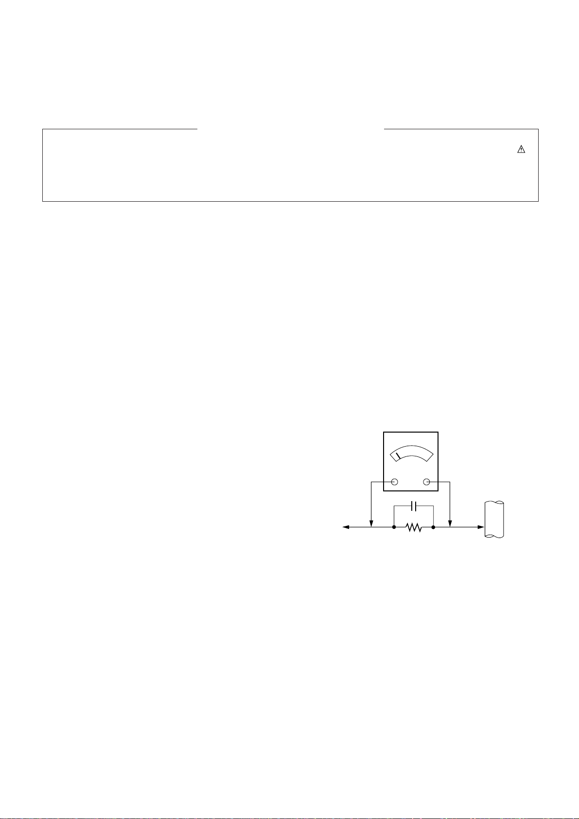
Leakage Current Hot Check (See below Figure)
Plug the AC cord directly into the AC outlet.
Do not use a line Isolation Transformer during this check.
Connect 1.5K/10watt resistor in parallel with a 0.15uF capacitor
between a known good earth ground (Water Pipe, Conduit, etc.)
and the exposed metallic parts.
Measure the AC voltage across the resistor using AC
voltmeter with 1000 ohms/volt or more sensitivity.
Reverse plug the AC cord into the AC outlet and repeat AC
voltage measurements for each exposed metallic part. Any
voltage measured must not exceed 0.75 volt RMS which is
corresponds to 0.5mA.
In case any measurement is out of the limits specified, there is
possibility of shock hazard and the set must be checked and
repaired before it is returned to the customer.
Leakage Current Hot Check circuit
1.5 Kohm/10W
To Instrument's
exposed
METALLIC PARTS
Good Earth Ground
such as WATER PIPE,
CONDUIT etc.
AC Volt-meter
IMPORTANT SAFETY NOTICE
0.15uF
Page 4
- 4 -
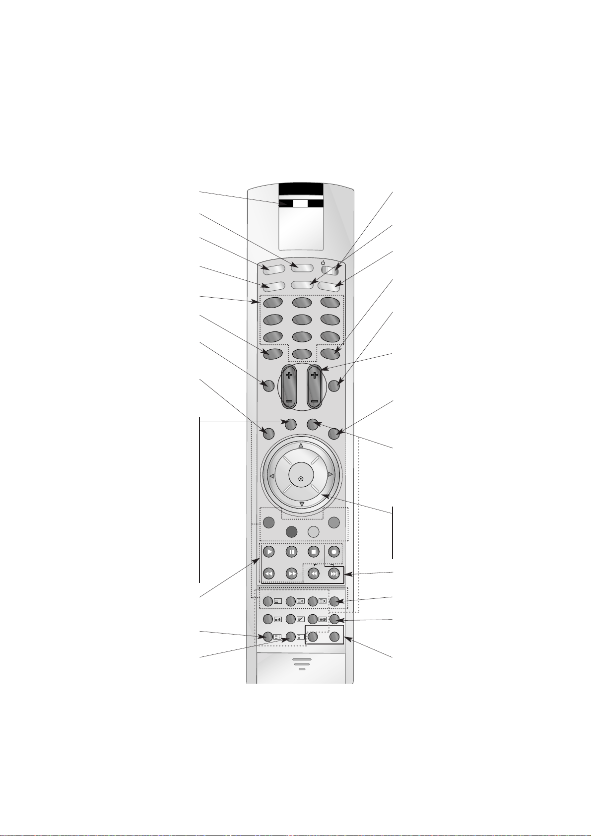
DESCRIPTION OF CONTROLS
123
456
789
0
DVD
STB
AUDIO
MODE
POWER
MUTE
TV/AV
MULTIMEDIA
ARC
SSM
Q.VIEW
PSM
FAVOURITE
MENU
PIP PR-
PIP ARC
LIST
PLAY
REW FF SKIP
PAUSE STOP
RECORD
ZOOM- ZOOM+
SPLIT ZOOM
SLEEP
I/II
WIN.SIZE
WIN.POSITION
PIP INPUT
PIP PR+ SWAP
OK
PIP/DW TEXT
EXIT
PR
VOL
CABLE
VCR
?
M
TV
Displays the selected device.
TV/AV
Selects the TV, AV, Component, RGB
or DVI modes.
MODE
Selects another device.
NUMBER buttons
PIP/DW
Switches the sub picture on or off.
Selects PIP or DW modes.
PIP PR + /-
Selects a program for the sub picture.
SWAP
Alternates between main and sub pic-
ture.
PIP INPUT
Selects the input mode for the sub pic-
ture.
WIN.SIZE
Adjusts the sub picture size.
WIN.POSITION
Moves the sub picture to
DD/ EE
or FF/
GG
direction.
PIP ARC
Changes the picture format for the
sub picture.
OK
accepts your selection or displays the
current mode.
DD/ EE
or FF/
GG
Adjusts menu settings.
Selects menu item.
POWER
switches the set on from standby or
off to standby.
ARC
Changes the picture format.
MUTE
Switches the sound on or off.
Q.VIEW
Returns to the previously viewed
programme.
SSM
To select the sound appropriate to
your viewing programme character.
VOL +/- (Volume Up/Down)
Increases/decreases sound level.
PR +/- (Programme Up/Down)
selects a programme.
EXIT
Clears all on-screen displays and
returns to TV viewing from any
menu.
DVD BUTTONS
Controls a LG DVD player.
SLEEP
Sets the sleep timer.
I/II
Selects the language during dual language broadcast.
Selects the sound output.
ZOOM+ / ZOOM-
Enlarges or reduces the main picture
size.
TEXT
These buttons are used for teletext.
For further details, see the ‘Teletext’
section.
Note : In teletext mode, the PIP PR
+/-, SWAP and PIP INPUT buttons are
used for teletext function.
MULTIMEDIA
Selects the Component, RGB or DVI
modes.
FAVOURITE
selects a favorite programme.
PSM
Adjusts the factory preset picture
according to the room.
MENU
Displays on screen menus one by one.
Exits the current menu.
Memorizes menu changes.
VCR BUTTONS
Controls a LG video cassette
recorder.
LIST
Displays the program table.
SPLIT ZOOM
Enlarge the screen with regular
ration.
Page 5
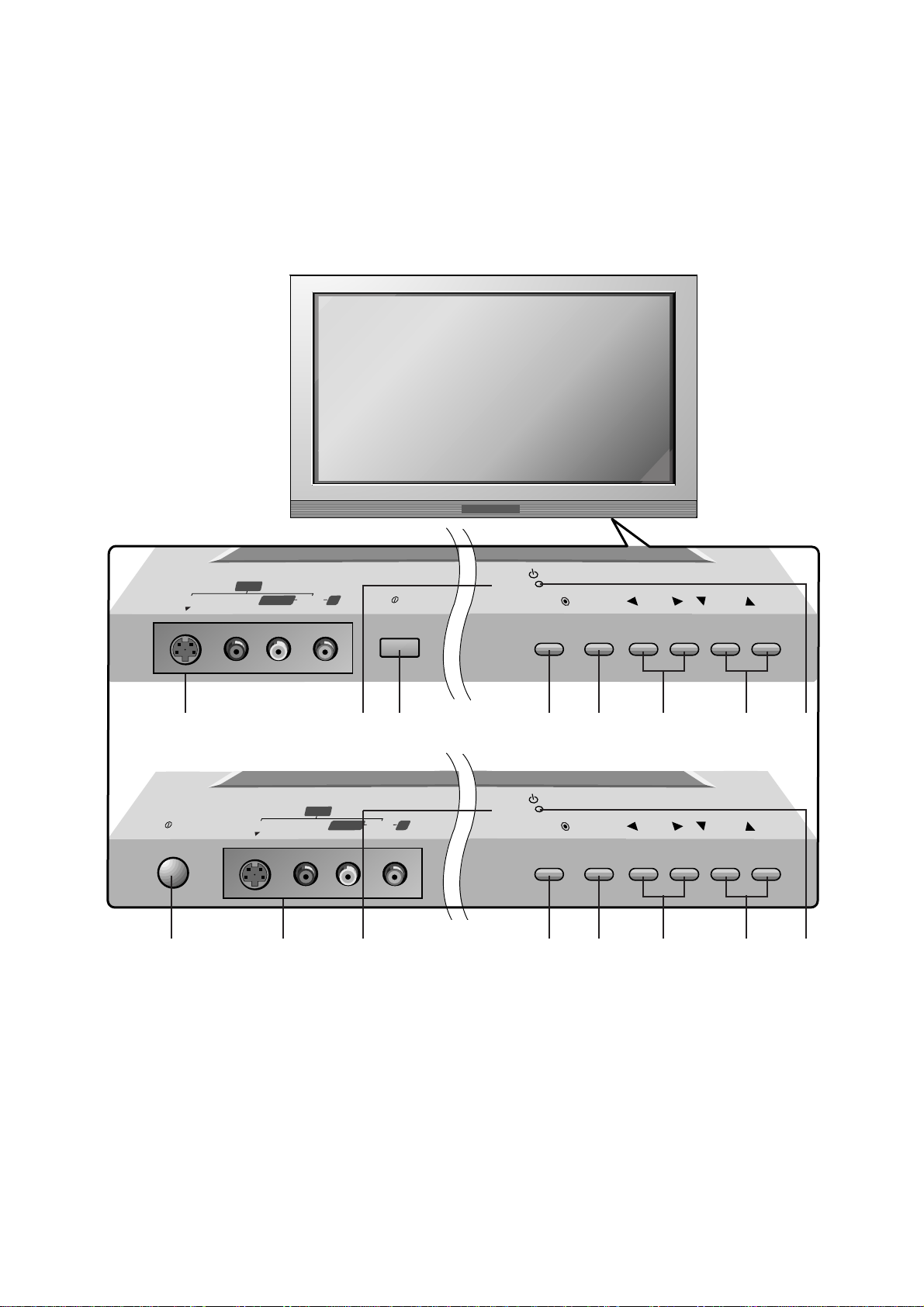
- 5 -
1.
AUDIO/VIDEO IN SOCKETS
S-VIDEO/AUDIO IN SOCKETS
2.
Remote Control Sensor
3. Main Power Button
4. TV/AV Button
Selects the TV, AV, Component, RGB or DVI modes.If OSD is
displayed, selects menu item.
5. MENU Button
6.
FF/ GG
(Volume Up/Down) Buttons
7.DD/EE(Programme Up/Down) Buttons
8. Power Standby Indicator
Illuminates red in standby mode, Illuminates green when the
set is turned on
<Front Panel Controls>
ON/OFFS-VIDEO VIDEO AUDIO
L/MONO
AV4
R
TV/AV
MENU
VOL
PR
S-VIDEO VIDEO AUDIO
L/MONO
AV4
R
TV/AV
MENU
VOL
PR
ON/OFF
- Shown is a simplified representation of the set.
- Here shown may be somewhat different from your set.
1 2 3 4
or
5 6 7 8
1 23 4 5 6 7 8
Page 6
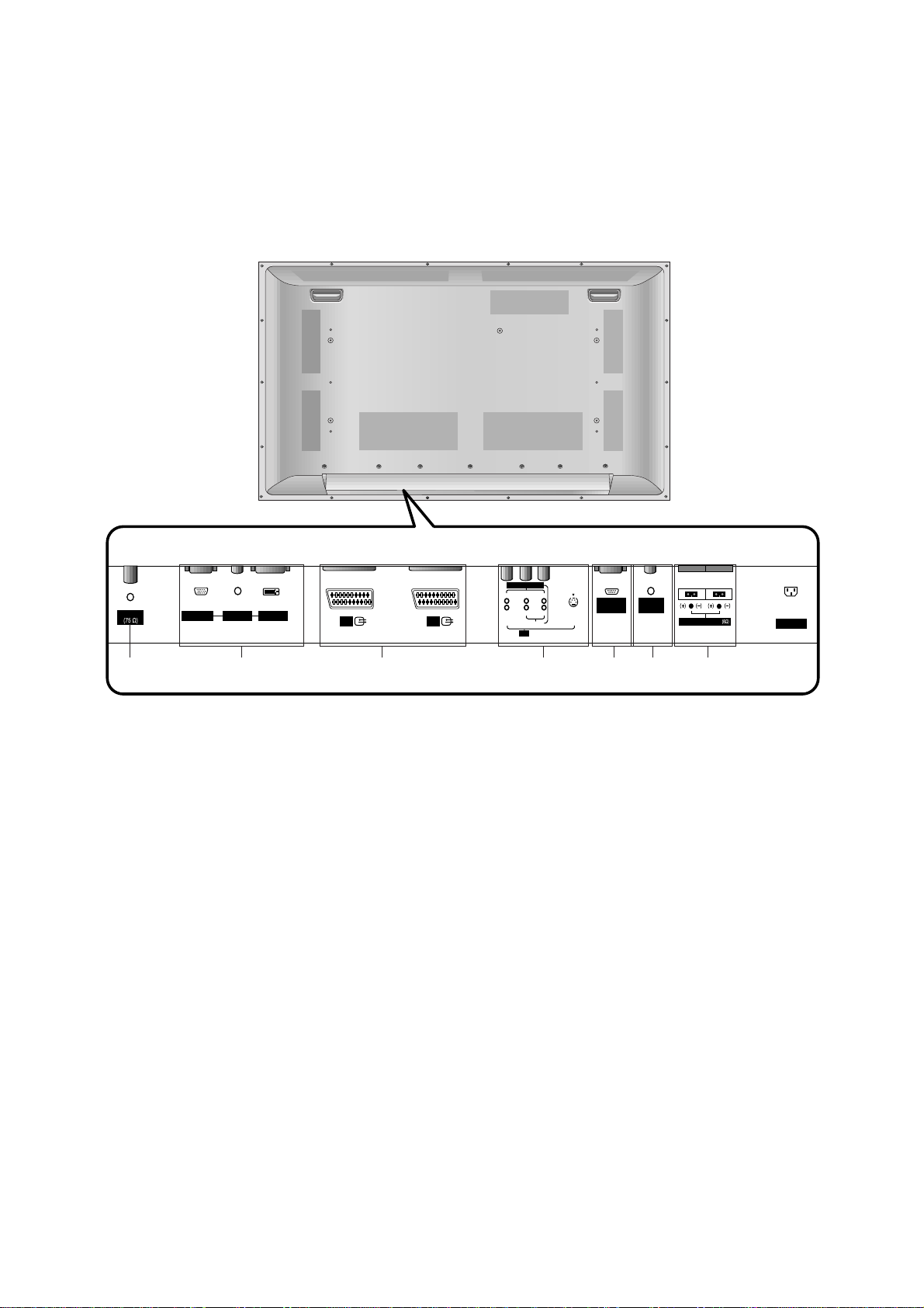
- 6 -
Location and Function of Controls
Location and Function of Controls
<Back Panel>
Antenna
RGB INPUT DVI INPUT
AV1
AUDIO INPUT
AV2
COMPONENT
AV3
Y P
B
L
(MONO)
AUDIO S-VIDEOVIDEO
R
P
R
RS-232C INPUT
EXTERNAL SPEAKER
R L
CONTROL
REMOTE
(CONTROL/SERVICE)
AC INPUT
1. ANTENNA INPUT
2. RGB INPUT / AUDIO INPUT / DVI INPUT
Connect the monitor output socket of the PERSONAL COMPUTER to this socket.
3. EURO SCART SOCKET
Connect the euro scart socket of the VCR to these sockets.
4. COMPONENT INPUT
AUDIO/VIDEO IN SOCKETS (AV3)
Connect the audio/video out sockets of external equipment to
these sockets.
S-VIDEO/AUDIO IN SOCKETS
Connect the S-VIDEO out socket of an VCR to the S-VIDEO
socket.
Connect the audio out sockets of the VCR to the audio sockets as in AV3.
5. RS-232C INPUT(CONTROL/SERVICE) PORT
Connect to the RS-232C port on a PC.
6. CONTROL LOCK / REMOTE CONTROL
7. EXTERNAL SPEAKER OUTPUT (8 ohms)
Connect to optional external speaker(s).
* For further information, refer to ‘Speaker & Speaker Stand’
manual.
1 2 3 4 5 6 7
Page 7
- 7 -
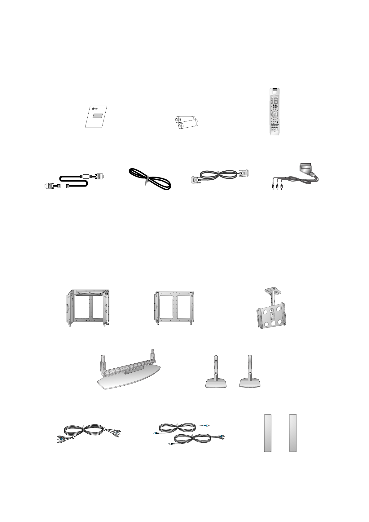
D-sub 15 pin cable
AS mark
LG TV
Owner’s Manual
1.5V
1.5V
Alkaline batteries
Power Cord
1 2 3
4 5 6
7 8 9
0
DVD
STB
AUDIO
MODE
POWER
MUTE
TV/AV
MULTIMEDIA
ARC
SSM
Q.VIEW
PSM
FAVOURITE
MENU
PIP PR-
PIP ARC
LIST
PLAY
REW FF SKIP
PAUSE STOP
RECORD
ZOOM- ZOOM+
SPLIT ZOOM
SLEEP
I/II
WIN.SIZE
WIN.POSITION
PIP INPUT
PIP PR+ SWAP
OK
PIP/DW TEXT
EXIT
PR
VOL
CABLE
VCR
?
M
TV
Remote Control handset
DVI-D Cable
Accessories
- Optional extras can be changed or modified for quality improvement without any notification new optional extras can be
added.
- Contract your dealer for buying these items.
Optional Extras
Phone scart cable (Optional)
Tilt wall mounting bracket
Video cables Audio cables
Desktop stand
Wall mounting bracket Ceiling mounting bracket
Speakers
Desktop Speaker stand
Page 8

- 8 -
SPECIFICATIONS
NOTE : Specifications and others are subject to change without notice for improvement
.
V Scope
This specification can be applied to all model of 50”PDP TV related to RF-03OB Chassis.
V Test Condition
1) Temperature : 25±5°C (77±9°F)
2) Relative Humidity: 65±10%
3) Power Voltage:Standard Input Voltage
(AC 110V-240V~, 50/60Hz)
But Standard input voltage mark value is marked by model.
4) Follow each drawing or spec for spec and performance of parts,based upon P/N of RPL
5)
Warm up set for more than 20min before the
measurement.
V Test and Inspection Method
1) Performance : Follow the Standard of LG TV test
2) Extra standards
Safety: Follow the standard of CE, IEC
EMC : Follow the standard of CE, IEC
Remark
Safety : IEC60065, IEC60095
EMI : EN55013
EMS : EN55020
Safety : IEC60065, IEC60095
EMI : EN55013
Model Name
RZ-42PZ70
RT-42PZ70
Market
EU
N-EU
Chassis
RF-03OA
Model Name
RZ-50PZ60/70
RT-50PZ60/70
Market Place
EU
N-EU
Brand
LG
LG
Page 9

1. Application Object
These instructions are applied to all of the PDP monitor/
Tuner , RF-03OB chassis.
2. Notes
(1) Because this is not a hot chassis, it is not necessary to use
an isolation transformer. However, the use of isolation
transformer will help protect test instrument.
(2) Adjustment must be done in the correct order.
(3) The adjustment must be performed in the circumstance of
25±5°C of temperature and 65±10% of relative humidity if
there is no specific designation.
(4) The input voltage of the receiver must keep 220V, 60Hz in
adjusting.
(5) The receiver must be operated for about 15 minutes prior
to the adjustment.
¤ After receiving 100% white pattern, the receiver must be
operate prior to adjustment.(Or white condition in HEATRUN mode)
¤ŁEnter into HEAT-RUN mode
- Select the HEAT-RUN OFF by pressing ADJ Key on
Remote Control for adjustment.
- Press the VOL + Key in HEAT-RUN OFF.
(OSD display HEAT-RUN WHITE and screen display
100% FULL WHITE PATTERN)
[ Set is activated HEAT-RUN without signal generator in
this mode.
[ Single color pattern of HEAT-RUN mode uses to check
PANEL.(RED/BLUE/GREEN)
If you turn on a still screen more than 20 minutes, a
afterimage may be occur in the black level part of the
screen.
3. Board Adjustment Method
<Channel memory>
(1) Input the power to VSC board.
(2) Connect the PC for channel memory work to VSC board
whit RS-232C.
(3) Execute the program for channel memory that fit each
BOM
- Method to execute program for channel memory
¤ Click the “CHANNEL(RF03OA_B).EXE” to execution.
¤ŁSelect the setting PORT of PC in”SELECT PORT” and
then click the “SELECT PORT”.
¤ØClick the “DOWN LOAD TO E2PROM”
¤ŒClick the “OPEN“ in FILE NAME
¤ºClick a suitable data on BOM.
¤ºClick the “ENTER”
¤ Show the channel memory.
¤ When the channel memory is finished, divide the RS-
232C CABLE in VSC BOARD.
¤ In case VSC BOARD of same BOM, connect the RS-
232C CABLE and then repeat ¤º~¤ by same method.
4. RGB Auto Cut-Off & MIN Bia
Adjustment
(1) Input Full White (255 Gray) signal which generated from
Pattern Generator into RGB1 Input part.
(2) Press POWER ON KEY on R/C for adjustment and select
AUTO-CUT(Cut-off Auto Adjustment)
(3) Press Vol. + key and operate TO SET
(4) Screen adjustment starts with Full Black screen.
Original Full White screen will be presented about 3-5
seconds later. And if there is a mark of OK OSD, then the
Auto Cut-off and Min-Bias adjustment will be completed.
(5) Pass to the next MAX Bias Adjustment after Adjustment.
O You can check whether circuit adjustment is operated well or
not, as below.
(1) Display RGB to the Main picture, AV to the Sub picture in
the TWIN PICTURE.
(2) To check the MIN-Bias, input Full Black (0 gray) signal into
AV and RGB input part at the same time in the Pattern
Generator.
(3) To check the MAX-Bias, input Full White (255 gray) signal
into AV and RGB input part at the same time in the Pattern
Generator.
(4) Compare Black Level with White Level by eyes. And if
there is no Level difference, the adjustment is completed
well.
O Data value, which adjusted in the board, is valid until the VSC
Board is disuse and must be protected. For the protection of
data, Micom does not permit any more adjustment after
completion.
O In case of re-adjustment, operate First Value Setting.
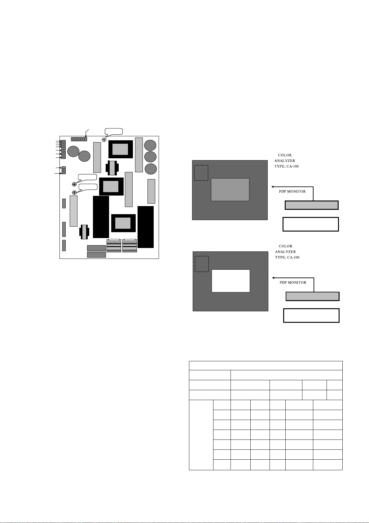
5. POWER PCB Assy Voltage
Adjustment (Va, Vs, Voltage Adjustment)
5-1. Test Equipment
: D.M.M 1EA
5-2. Connection Diagram for Measuring
: refer to<fig 1>
5-3. Adjustment Method
(1) Va Adjustment
¤ After receiving 100% white pattern, HEAT RUN.
¤Ł Connect + terminal of D.M.M to Va pin of P805 and
connect – terminal to GND pin of P805.
¤Ø After turning the VR351, voltage of D.M.M adjustment
as same as Va voltage which on label of panel
Right/Top. (Deviation : ±0.5V)
- 9 -
ADJUSTMENT INSTRUCTIONS
Each PCB Assy must be checked by the Check JIG Set before
whole assembly. (Be careful the POWER PCB Assy not to
damage to PDP Module)
Page 10
(2) Vs Adjustment
¤ Connect + terminal of D.M.M to Vs pin of P805 and
connect – terminal to GND pin of P805.
¤Ł After turning the VR551, voltage of D.M.M adjustment
as same as Vs voltage which on label of panel
Right/Top. (Deviation : ±0.5V)
(3) 5.2V Adjustment
¤ Connect + terminal of D.M.M to 5V pin of P804 and
connect – terminal to GND pin of P804.
¤Ł Turning VR251, adjust the volt value to 5.2v value.
6. Adjustment of White Balance
6-1. Required Equipment
Color analyzer (CA-100 or same product)
6-2. Connection Diagram of Equipment for
Measuring (Manual Adjustment)
: refer to <fig 2>,<fig 3>
6-3. Adjustment of White Balance
O Operate the Zero-calibration of the CA-100, then stick
sensor to PDP module surface when you adjust.
O For manual adjustment, it is also possible by the following
sequence.
(1) Select WHITE PATTERN of HEAT RUN mode by pressing
POWER ON KEY on remote control for adjustment then
operate HEAT RUN more than 15 minute.
(2) Supply 70Gray, 216Gray Level, 100% size length and
breadth signal to AV input. (Refer to <fig 2>,<fig 3>)
RZ-50PZ60/70 : AV3, RT-50PZ60/70 : AV1
(3) White balance is adjusted from Low Light to High Light,
And pushing the V key, save the adjustment value.
(4) LOW Light, stick sensor to 70Gray Pattern and then press
ADJ Key on R/C for adjustment and press
D, E on R/C in
adjustment mode to select R-L or G-L, press VOL +, - Key
and adjust it until color coordination becomes as below.
[RZ-50PZ60/70, RT-50PZ60/70]
X: 0.285±0.003, Y: 0.285±0.003
Color temperature: 9,700°K±500°K
(5) High Light, stick sensor to 216Gray Pattern and then press
ADJ Key on R/C for adjustment and press
D, E on R/C in
adjustment mode to select R-H or G-H, press VOL +, - Key
and adjust it until color coordination becomes as below.
[RZ-42PZ70, RT-42PZ70]
X: 0.285±0.003, Y: 0.285±0.003
Color temperature: 9,700°K±500°K
(6) Exit adjustment mode using V Key.
7.
Map for Auto adjustment (RS-232C)
- 10 -
Va ADJ
VR351
Vs ADJ
VR551
CN 804
P805
P804
P803
P802
P801
VS
Va
Va
GND
GND
VS
VS
5V
GND
Va ADJ
VR251
<Fig 1> Connection Diagram for Measuring of Power Adjustment
Typ
Baud Rate
1150200
Index
R-L
G-L
R-H
G-H
Data bit
8
Cmd1 Cmd2
j j
j k
j a
j b
Stop bit1Parity
NONE
RF-03OB_PDP50
Protocol
Setting
Data Min Value
54(36)
54(36)
180(B4)
170(A4)
Max Value
90(5A)
85(FA)
254(FE)
250(FA)
RS232
R-L 70 R-L 70
G-L 70 G-L 70
R-M 128 R-M 128
G-M 128 G-M 128
R-H 216 R-H 216
G-H 216 G-H 216
Window
MSPG-2100 or
MSTG-5200
RGB Signal Input
High Light adjustment
70 Gray Level
<Fig 2> Low Light(Connection Diagram of Manual Adjustment)
R-L 70 R-L 70
G-L 70 G-L 70
R-M 128 R-M 128
G-M 128 G-M 128
R-H 216 R-H 216
G-H 216 G-H 216
Window
MSPG-2100 or
MSTG-5200
RGB Signal Input
High Light adjustment
216 Gray Level
<Fig 3> High Light (Connection Diagram of Manual Adjustment)
Page 11
- 11 -
8. Adjustment of Component Off-Set
8-1. Required Test Equipment
: HD-STB(SK-010T) or same product
8-2. Manual Adjustment of Component Off-
Set
(1) Input Video signal and Component 720P,1080i signal of
HD-STB.
(2) Press ADJ key of R/C twice for entering twin picture mode.
(3) Adjust the same color senses between main and sub,
using Volume +; -key of R/C in R, G, B Off-Set menu.
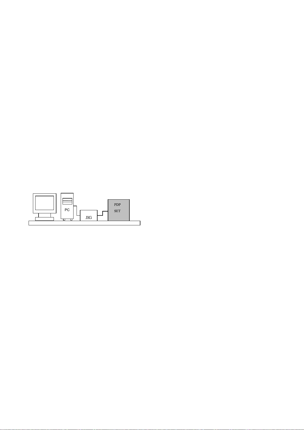
9. DDC Data input
9-1. Required Test Equipment
(1) A jig for adjusting PC, DDC. (PC serial to D-sub
Connection equipment)
(2) S/W for writing DDC(EDID data write & read)
(3) D-Sub 15P cable, D-Sub to DVI Connector (Connect to
DVI Jack)
9-2. Setting of Device
9-3. Preparation for Adjustment
(1) Set devices as above and turn the PC, jig on.
(2) Put S/W for writing DDC (EDID data write & read) into
operation. (operated in DOS mode.)
9-4. Sequence of Adjustment
(1) DDC Data Input for Analog-RGB
¤ Put the set on the table and turn the power on.
¤ŁConnect PC Serial to D-sub 15P Cable of JIG for DDC
Adjustment to RGB terminal (D-Sub 15Pin).
¤Ø Operate S/W for DDC record and select DDC Data for
Analog RGB in Model Menu.
¤Œ Operate EDID Write command.
¤º Operate EDID Read command and check whether
Check Sum is OK.
¤ If Check Sum is NG, repeat ¤Ø~ ¤Œ.
¤ If Check Sum is OK, DDC Data for Analog-RGB input is
completed.
(2) DDC Data input for Digital-RGB
¤ Connect PC Serial to DVI Cable of JIG for DDC
Adjustment to RGB2 terminal (DVI Jack).
¤Ł Operate S/W for DDC record and select DDC Data for
Digital RGB in Model Menu.
¤ØOperate EDID Write command.
¤Œ Operate EDID Read command and check whether
Check Sum is OK.
¤ºIf Check Sum is NG, repeat ¤Ø~ ¤Œ.
¤ If Check Sum is OK, DDC Data for Digital-RGB input is
completed.
* If you change the Booster 0 to 1 in a fringe area, a
user ca set to Booster “On”.
Page 12
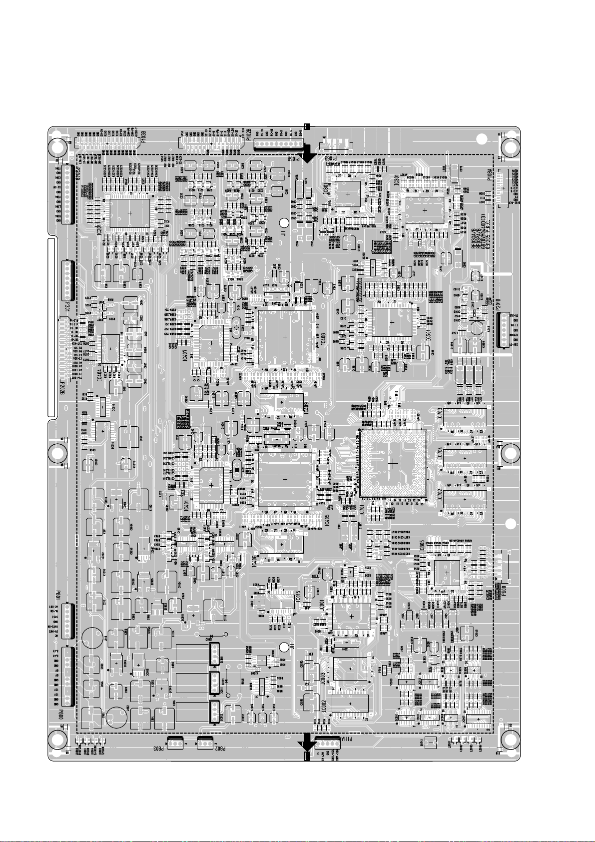
- 12 -
MAIN (TOP)
PRINTED CIRCUIT BOARD
Page 13

- 13 -
MAIN (BOTTOM)
Page 14

- 14 -
REAR AV (TOP) REAR AV (BOTTOM) FRONT AV (TOP)
FRONT AV (BOTTOM)
POWER SWITCH
Page 15

- 15 -
PREAMP (BOTTOM)
PREAMP (TOP)
SPEAKER (TOP)
SPEAKER (BOTTOM)
Page 16

- 16 -
TUNER (TOP)
Page 17

- 17 -
TUNER (BOTTOM)
Page 18

- 18 -
BLOCK DIAGRAM
cable
Page 19

MEMO
- 19 -
Page 20

- 20 -
EXPLODED VIEW
301
303
302
300
305
400
203
200
213
202
210
208
209
207
206
211
580
304
581
410
430
101
440
420
570
540
550
551
552
401
530
531
590
532
520
524
560
523
525
522
102
103
Page 21

- 21 -
EXPLODED VIEW PARTS LIST
101 5900V12001A FAN,DC G1225S12B2 DONGYANG 12X12X25 12V130MA 1500 168GM MOTOR L=260
102 4980V01017A SUPPORTER,FAN EGI RIGHT PDP DN-50PY10
103 4980V01018A SUPPORTER,FAN EGI LEFT PDP DN-50PY10
200 6348Q-C033S PDP,50 16:9 1365*768 PDP50X20330.AKLGG
201 6871QRH035B PWB(PCB) ASSEMBLY,DISPLAY XRRT ASSY HAND INSERT 50X2 BARE PCB
202 6871QPH008A PWB(PCB) ASSEMBLY,DISPLAY DCDC ASSY HAND INSERT KK MODEL
203 6871QZH031A PWB(PCB) ASSEMBLY,DISPLAY ZSUS ASSY HAND INSERT 50KK 2LAYER
205 6871QLH032B PWB(PCB) ASSEMBLY,DISPLAY XRLT ASSY HAND INSERT 50X2 BARE PCB 352.5 X 280
206 6871QXH021B PWB(PCB) ASSEMBLY,DISPLAY XRCB ASSY HAND INSERT 50X2 BARE PCB
207 6871QLH033B PWB(PCB) ASSEMBLY,DISPLAY XRLB ASSY HAND INSERT 50X2 BARE PCB 352.5 X 280
208 6871QDH049A PWB(PCB) ASSEMBLY,DISPLAY YDRV ASSY HAND INSERT 50WXDP2 4L(BTM)
209 6871QYH028A PWB(PCB) ASSEMBLY,DISPLAY YSUS ASSY HAND INSERT 50KK 4LAYER
210 6871QDH048A PWB(PCB) ASSEMBLY,DISPLAY YDRV ASSY HAND INSERT 50WXDP2 4L(TOP)
211 6871QRH036B PWB(PCB) ASSEMBLY,DISPLAY XRRB ASSY HAND INSERT 50X2 BARE PCB
212 6871QXH020B PWB(PCB) ASSEMBLY,DISPLAY XRCT ASSY HAND INSERT 50X2 BARE PCB
213 6871QCH028C PWB(PCB) ASSEMBLY,DISPLAY CTRL ASSY HAND INSERT 50X2 TMDS FOR 4022H
300 3091V00B68D CABINET ASSEMBLY,RT-50PZ60 NON RF03OB NON
3091V00B69E CABINET ASSEMBLY,RT-50PZ70 NON RF03OB NON
301 4980V00634A SUPPORTER,FILTER AL DN-50PZ60 TOP
302 4980V00636A SUPPORTER,FILTER AL DN-50PZ60
4980V00636B SUPPORTER,FILTER AL DN-50PZ70
303 4980V00637A SUPPORTER,FILTER AL DN-50PZ60 SIDE
304 4980V00374A SUPPORTER,MODULE EGI CENTER,MN-50PZ40
305 3790V00683C FILTER(MECH), - MN-50PZ41 1150G03EK NBK 50 MESH SINGLE GLASS FILTER
400 3809V00B03A BACK COVER ASSEMBLY,DN-50PZ60 NON NON
401 3301V00014E PLATE ASSEMBLY, AV 3300V00244 RP-50PZ60 C/SKD
410 4980V00790A SUPPORTER,MODULE AL DIE-CASTING DN-50PZ60 SUPP_MODULE ASSY
420 4980V00790B SUPPORTER,MODULE AL DIE-CASTING DN-50PZ60 SUPP.MODULE ASSY(R)
430 4980V00791C SUPPORTER,FAN EGI PRESS
440 4980V00792C SUPPORTER,FAN EGI PRESS
520 6871VMMS50A PWB(PCB) ASSEMBLY,MAIN RF-03OB 50KK ANALOG BUILT IN VSC B/D
6871VMMS49A PWB(PCB) ASSEMBLY,MAIN RF-03OB RT 50KK ANALOG BUILT IN VSC B/D
522 4814V00424A SHIELD,RZ-42PZ70 RF03OA ET ANALOG 2 TUNER TOP
523 4980V00641A SUPPORTER,NON SECC VSC_BOTTOM
524 4980V00642D SUPPORTER,VSC AL .
525 4814V00425A SHIELD,RZ-42PZ70 RF03OA ET ANALOG 2 TUNER BOTTOM
530 6871VSMF08A PWB(PCB) ASSEMBLY,SUB PSW AF03BA BUILT IN PDP
531 5020V00457A BUTTON, KEY BUTTON POWER FD-36X3
532 4810V00737A BRACKET,AV DN-50PZ60 AB00EA ABS, AF-303S PDP
540 6871VSMY20A PWB(PCB) ASSEMBLY,SUB A/V RF03OA RT-42PZ70 KK ANALOG 2TUNER B-IN
550 6871VSMX09A PWB(PCB) ASSEMBLY,SUB SPK RF03OB PDP 50 KK ANALOG BUILT IN SPEAKER B/D
551 4980V00647A SUPPORTER,NON AL DN-50PZ60 REAR A/V
552 4980V00962B SUPPORTER,NON SECC(EGI) RZ-50PZ70
560 6871VSMY70A PWB(PCB) ASSEMBLY,SUB,TUNER RF03OA RT SDA6001 42 50 PDP
570 6871VSMX31A PWB(PCB) ASSEMBLY,SUB,CONT RF03OB 50 KK ANALOG BUILT IN RZ-50PZ60/70
580 3501V00084D BOARD ASSEMBLY,POWER MN50PZ10 RF03GB SRX-75 SONY 50KK
581 3720V00237B PANEL,ASSY RZ-50PZ60 VFD 16ML07HA1 SDI VFD
590 6871VSMX08A PWB(PCB) ASSEMBLY,SUB A/V RF03FB 50 KK ANALOG BUILT IN FRONT B/D
No.
Description
Part No.
Page 22

REPLACEMENT PARTS LIST
LOCA. NO PART NO DESCRIPTION
IC704
IC801
IC805
IC902
IC903
IC904
IC905
IC906
IC907
IC908
IC909
IC910
IC911
IC912
IC913
IC914
IC915
IC203
IC204
Q001
Q001
Q001
Q002
Q002
Q002
Q003
Q003
Q004
Q004
Q005
Q006
Q101
Q102
Q103
Q104
Q105
Q106
Q107
Q108
Q109
Q110
Q201
Q202
Q203
Q204
Q205
Q206
Q207
Q208
Q209
Q210
0IMMRHY033A
0IPRPTI001A
0IS5160000A
0IMCRSJ001A
0IMCRFA010A
0IMCRRH001A
0IMCRRH001A
0IMCRSH001A
0IMCRSH001A
0IDS162100B
0IMCRPH015A
0IMCRKE007A
0ISS278120A
0IMCRKE007A
0ITK118100B
0IMCRRH001A
0IMCRRH001A
0TR830009BA
0TR830009BA
0TR387500AA
0TR387500AA
0TR830009BA
0TR387500AA
0TR387500AA
0TR830009BA
0TR387500AA
0TR830009BA
0TR387500AA
0TR830009BA
0TR387500AA
0TR150400BA
0TR150400BA
0TR387500AA
0TR387500AA
0TR150400BA
0TR387500AA
0TR387500AA
0TR150400BA
0TR387500AA
0TR150400BA
0TR150400BA
0TR387500AA
0TR387500AA
0TR387500AA
0TR387500AA
0TR387500AA
0TR387500AA
0TR387500AA
0TR387500AA
0TR387500AA
0TR387500AA
HY57V643220C(L)T-6 HYNIX 86P TSOP
TFP401PZP 100,TQFP
SIL160CT100 SILICON IMAGE 100 TQFP
SC1565IST-1.8 SEMTECH 3P SOT223
KA7809R, FAIRCHILD 2P D-PAK
BA033FP-E2 ROHM 3P-SOP,TO252-3
BA033FP-E2 ROHM 3P-SOP,TO252-3
PQ05DZ1U SHARP 5, SMD TYPE
PQ05DZ1U SHARP 5, SMD TYPE
DS1621V 8P SOIC ST THERMOSTAT
74LVC32AD PHILIPS 14P SOT108-1
KIA278R09PI KEC TO220IS,4P ST 2A
KA278R12 4P,TO-220F
KIA278R09PI KEC TO220IS,4P ST 2A
TK11840L 8P SOT23L
BA033FP-E2 ROHM 3P-SOP
BA033FP-E2 ROHM 3P-SOP
BSS83 TP PHILIPS
BSS83 TP PHILIPS
CHIP 2SC3875S(ALY) KEC
CHIP 2SC3875S(ALY) KEC
BSS83 TP PHILIPS
CHIP 2SC3875S(ALY) KEC
CHIP 2SC3875S(ALY) KEC
BSS83 TP PHILIPS
CHIP 2SC3875S(ALY) KEC
BSS83 TP PHILIPS
CHIP 2SC3875S(ALY) KEC
BSS83 TP PHILIPS
CHIP 2SC3875S(ALY) KEC
CHIP 2SA1504S(ASY) KEC
CHIP 2SA1504S(ASY) KEC
CHIP 2SC3875S(ALY) KEC
CHIP 2SC3875S(ALY) KEC
CHIP 2SA1504S(ASY) KEC
CHIP 2SC3875S(ALY) KEC
CHIP 2SC3875S(ALY) KEC
CHIP 2SA1504S(ASY) KEC
CHIP 2SC3875S(ALY) KEC
CHIP 2SA1504S(ASY) KEC
CHIP 2SA1504S(ASY) KEC
CHIP 2SC3875S(ALY) KEC
CHIP 2SC3875S(ALY) KEC
CHIP 2SC3875S(ALY) KEC
CHIP 2SC3875S(ALY) KEC
CHIP 2SC3875S(ALY) KEC
CHIP 2SC3875S(ALY) KEC
CHIP 2SC3875S(ALY) KEC
CHIP 2SC3875S(ALY) KEC
CHIP 2SC3875S(ALY) KEC
CHIP 2SC3875S(ALY) KEC
LOCA. NO PART NO DESCRIPTION
IC001
IC001
IC002
IC002
IC003
IC003
IC003
IC004
IC004
IC005
IC005
IC006
IC006
IC007
IC007
IC008
IC009
IC010
IC011
IC012
IC013
IC014
IC015
IC016
IC101
IC107
IC201
IC201
IC202
IC202
IC203
IC205
IC301
IC401
IC402
IC403
IC404
IC405
IC406
IC407
IC408
IC409
IC501
IC601
IC603
IC604
IC605
IC606
IC701
IC702
IC703
0IMCRMN023A
0IMCRRS001A
0IMMRHY001F
0IMMRSS064A
0IZZVA0087A
0IMMRSG028A
0IMMRMR006B
0IMCRAL006A
0IMMRAL025A
0IKE702700D
0IMCRFA013A
0ISJ111733A
0IMCRFA013A
0ISJ111725A
0ITI745740M
0IMCRPH017A
0IPH740800L
0IMCRPH015A
0IMCRPH016A
0IMCRPH014A
0IKE702700D
0IDS232000A
0IPH858400A
0IMCRTI001A
0IMI623200B
0ISA428200A
0ISO206900A
0IMCRTI003A
0IAL242110A
0IMCRFA010A
0IAL242110A
0IMCRTI003A
0IMCRAD003A
0IIT323000E
0IFA741230A
0IFA741230A
0IMCRMI006A
0IMCRGN001B
0IMMRHY033A
0IIT323000E
0IMCRGN002B
0IMMRHY033A
0ISO210100B
0IMCRMN004C
0IMCRFA009A
0IMCRFA015A
0IKE704200J
0IMCRSH001A
0IMCROT001B
0IMMRHY033A
0IMMRHY033A
SDA6001 QH B12 MICRONAS 128P
R8820LV RDC 100P PQFP
HY57V641620HGT-H HYNIX 54P
K6R4016V1D-TC10 44P
M37272E8A(OTP) DIP 42P ST
M27V160 STM 42P PDIP ST
MX29LV160ATTC-70 MACRONIX 48P
AT24C16AN-10SI-2.7 ATMEL 8P
AT24C32AN-10SI-2.7 ATMEL 8PIN
KIA7027AF 3, SOT-89 TP
74LCX244MTC FAIRCHILD 20P TSSOP
EZ1117CST-3.3 3P,SOT-223 TP 3.3V
74LCX244MTC FAIRCHILD 20P TSSOP
EZ1117ACST-2.5 3P SOT ST
SN74HC574NSR 14P,SOP
74LVC574APW PHILIPS 20P SOT360-1
74LVT08D 14SOP
74LVC32AD PHILIPS 14P SOT108-1
74LVC139D PHILIPS 16P SOT109-1
74LV132D PHILIPS 14P SOT108-1
KIA7027AF 3, SOT-89 TP
DS232AS 16P,SOP TP RS-232
PCF8584T 20P,SOP TP
SN74HCT157D TEXAS INSTRUMENT 16P
M62320FP,I/O EXPANDER 16P
LA4282 12S 2CHX10W
CXA2069Q QFP64 BK I2C
SN74HCT08D TEXAS INSTRUMENT 16P
AT24C21-10SI-2.5 8P,SOP TP 1K
KA7809R, FAIRCHILD 2P D-PAK
AT24C21-10SI-2.5 8P,SOP TP
SN74HCT08D TEXAS INSTRUMENT 16P
AD9888KS-140 ANALOG DEVICE 128P
VPC3230D C5 80P QFP
DM74LS123MX 16SOP TP
DM74LS123MX 16SOP TP
M52758FP MITSUBISHI 36PIN
FLI2310BC GENESIS 208P PQFP
HY57V643220C(L)T-6 HYNIX 86P TSOP
VPC3230D C5 80P QFP
FLI2300BC GENESIS 208P PQFP
HY57V643220C(L)T-6 HYNIX 86P TSOP
CXA2101AQ 80P,QFP BK
MSP3451G C12 MICRONAS 80P PQFP
KA78M08RTM, FAIRCHILD 2P D-PAK
KA7805R FAIRCHILD 2P D-PAK
KIA7042AF SOT-89 TP 4.2V
PQ05DZ1U SHARP 5, SMD TYPE
REMBRANT-102 352P PBGA
HY57V643220C(L)T-6 HYNIX 86P TSOP
HY57V643220C(L)T-6 HYNIX 86P TSOP
IC
TRANSISTOR
- 22 -
Page 23

- 23 -
LOCA. NO PART NO DESCRIPTION
Q211
Q212
Q213
Q214
Q215
Q216
Q217
Q218
Q219
Q220
Q221
Q222
Q223
Q224
Q225
Q226
Q227
Q228
Q229
Q230
Q231
Q232
Q233
Q234
Q235
Q236
Q237
Q238
Q239
Q240
Q241
Q242
Q243
Q244
Q245
Q246
Q247
Q248
Q249
Q601
Q602
Q603
Q604
Q605
Q606
Q901
Q902
Q903
D001
D002
0TR387500AA
0TR387500AA
0TR387500AA
0TR387500AA
0TR387500AA
0TR387500AA
0TR387500AA
0TR387500AA
0TR388109AA
0TR388109AA
0TR388109AA
0TR388109AA
0TR388109AA
0TR388109AA
0TR387500AA
0TR387500AA
0TR387500AA
0TR387500AA
0TR387500AA
0TR387500AA
0TR387500AA
0TR387500AA
0TR150400BA
0TR387500AA
0TR104009AF
0TR150400BA
0TR150400BA
0TR150400BA
0TR387500AA
0TR387500AA
0TR387500AA
0TR387500AA
0TR387500AA
0TR387500AA
0TR150400BA
0TR387500AA
0TR104009AF
0TR387500AA
0TR387500AA
0TR150400BA
0TR387500AA
0TR387500AA
0TR387500AA
0TR150400BA
0TR150400BA
0TR830009BA
0TR830009BA
0TRKE80038A
0DD226239AA
0DD226239AA
CHIP 2SC3875S(ALY) KEC
CHIP 2SC3875S(ALY) KEC
CHIP 2SC3875S(ALY) KEC
CHIP 2SC3875S(ALY) KEC
CHIP 2SC3875S(ALY) KEC
CHIP 2SC3875S(ALY) KEC
CHIP 2SC3875S(ALY) KEC
CHIP 2SC3875S(ALY) KEC
KTC3881 CHIP KEC
KTC3881 CHIP KEC
KTC3881 CHIP KEC
KTC3881 CHIP KEC
KTC3881 CHIP KEC
KTC3881 CHIP KEC
CHIP 2SC3875S(ALY) KEC
CHIP 2SC3875S(ALY) KEC
CHIP 2SC3875S(ALY) KEC
CHIP 2SC3875S(ALY) KEC
CHIP 2SC3875S(ALY) KEC
CHIP 2SC3875S(ALY) KEC
CHIP 2SC3875S(ALY) KEC
CHIP 2SC3875S(ALY) KEC
CHIP 2SA1504S(ASY) KEC
CHIP 2SC3875S(ALY) KEC
CHIP KRC104S SOT-23 TP KEC
CHIP 2SA1504S(ASY) KEC
CHIP 2SA1504S(ASY) KEC
CHIP 2SA1504S(ASY) KEC
CHIP 2SC3875S(ALY) KEC
CHIP 2SC3875S(ALY) KEC
CHIP 2SC3875S(ALY) KEC
CHIP 2SC3875S(ALY) KEC
CHIP 2SC3875S(ALY) KEC
CHIP 2SC3875S(ALY) KEC
CHIP 2SA1504S(ASY) KEC
CHIP 2SC3875S(ALY) KEC
CHIP KRC104S SOT-23 TP KEC
CHIP 2SC3875S(ALY) KEC
CHIP 2SC3875S(ALY) KEC
CHIP 2SA1504S(ASY) KEC
CHIP 2SC3875S(ALY) KEC
CHIP 2SC3875S(ALY) KEC
CHIP 2SC3875S(ALY) KEC
CHIP 2SA1504S(ASY) KEC
CHIP 2SA1504S(ASY) KEC
BSS83 TP PHILIPS
BSS83 TP PHILIPS
KTC3552T-RTK KEC
CHIP KDS226 SOT-23
CHIP KDS226 SOT-23
LOCA. NO PART NO DESCRIPTION
D003
D004
D005
D006
D007
D008
D009
D010
D1101
D1102
D201
D207
D208
D209
D210
D211
D212
D213
D214
D215
D216
D217
D218
D219
D220
D221
D223
D225
D226
D227
D228
D229
D230
D601
D602
D603
D604
D904
D905
D906
D907
D908
D909
D910
D911
D912
LD001
LD001
LD002
LD003
LD004
LD901
0DD226239AA
0DD226239AA
0DD226239AA
0DD226239AA
0DD226239AA
0DD226239AA
0DD226239AA
0DD226239AA
0DD100009AC
0DD184009AA
0DD226239AA
0DD226239AA
0DD226239AA
0DD226239AA
0DD226239AA
0DD226239AA
0DD226239AA
0DD226239AA
0DD226239AA
0DD226239AA
0DD226239AA
0DD226239AA
0DD226239AA
0DD226239AA
0DD226239AA
0DD226239AA
0DD184009AA
0DD226239AA
0DD226239AA
0DD226239AA
0DD226239AA
0DD226239AA
0DD226239AA
0DD184009AA
0DD184009AA
0DD226239AA
0DD226239AA
0DD226239AA
0DD226239AA
0DD226239AA
0DD226239AA
0DD226239AA
0DD226239AA
0DD226239AA
0DD226239AA
0DD110009DB
0DL200000CA
0DL233309AC
0DL233309AC
0DL233309AC
0DL233309AC
0DL233309AC
CHIP KDS226 SOT-23
CHIP KDS226 SOT-23
CHIP KDS226 SOT-23
CHIP KDS226 SOT-23
CHIP KDS226 SOT-23
CHIP KDS226 SOT-23
CHIP KDS226 SOT-23
CHIP KDS226 SOT-23
RU1V(1) TP SANKEN
KDS184S CHIP 85V 300MA KEC TP
CHIP KDS226 SOT-23
CHIP KDS226 SOT-23
CHIP KDS226 SOT-23
CHIP KDS226 SOT-23
CHIP KDS226 SOT-23
CHIP KDS226 SOT-23
CHIP KDS226 SOT-23
CHIP KDS226 SOT-23
CHIP KDS226 SOT-23
CHIP KDS226 SOT-23
CHIP KDS226 SOT-23
CHIP KDS226 SOT-23
CHIP KDS226 SOT-23
CHIP KDS226 SOT-23
CHIP KDS226 SOT-23
CHIP KDS226 SOT-23
KDS184S CHIP 85V 300MA KEC TP
CHIP KDS226 SOT-23
CHIP KDS226 SOT-23
CHIP KDS226 SOT-23
CHIP KDS226 SOT-23
CHIP KDS226 SOT-23
CHIP KDS226 SOT-23
KDS184S CHIP 85V 300MA KEC TP
KDS184S CHIP 85V 300MA KEC TP
CHIP KDS226 SOT-23
CHIP KDS226 SOT-23
CHIP KDS226 SOT-23
CHIP KDS226 SOT-23
CHIP KDS226 SOT-23
CHIP KDS226 SOT-23
CHIP KDS226 SOT-23
CHIP KDS226 SOT-23
CHIP KDS226 SOT-23
CHIP KDS226 SOT-23
RM11CV(1) TP SANKEN TP SANKEN
LED,SAM5670(DL-2LRG) BK Y-GREEN
LED,SAM2333 TP
LED,SAM2333 TP
LED,SAM2333 TP
LED,SAM2333 TP
LED,SAM2333 TP
DIODE
Page 24

- 24 -
LOCA. NO PART NO DESCRIPTION
LD902
LD903
LD904
ZD201
ZD202
ZD831
ZD832
ZD833
ZD834
C002
C004
C008
C009
C010
C011
C012
C020
C023
C026
C028
C030
C032
C034
C035
C036
C040
C044
C045
C046
C047
C051
C052
C1000
C1001
C1002
C1003
C1004
C1005
C1006
C101
C102
C1020
C103
C1034
C104
C104
C104
C104
C1047
C1048
0DL233309AC
0DL233309AC
0DL233309AC
0DZRM00178A
0DZRM00178A
0DR050008AA
0DR050008AA
0DR050008AA
0DR050008AA
0CE4763F618
0CE106SF6DC
0CE106SF6DC
0CE106SF6DC
0CE106SF6DC
0CE106SF6DC
0CE106SF6DC
0CE106SF6DC
0CE106SF6DC
0CE106SF6DC
0CE106SF6DC
0CE105SK6DC
0CE106SF6DC
0CE476SF6DC
0CE106SF6DC
0CE105SK6DC
0CE106SF6DC
0CE107SF6DC
0CE107SF6DC
0CE106SF6DC
0CE106SF6DC
0CE477VF6DC
0CE476SF6DC
0CE476SF6DC
0CE107SF6DC
0CE107SF6DC
0CE107SF6DC
0CE107SF6DC
0CE107SF6DC
0CE107SF6DC
0CE108DK61A
0CE108DK61A
0CE477WF6DC
181-120K
0CE477VF6DC
0CE476DF618
0CE474SK6DC
181-120K
0CE475SK6DC
0CE476SF6DC
0CE476SF6DC
LED,SAM2333 TP
LED,SAM2333 TP
LED,SAM2333 TP
UDZS TE-17 5.1B ROHM
UDZS TE-17 5.1B ROHM
SD05.TC R/TP SEMTECH
SD05.TC R/TP SEMTECH
SD05.TC R/TP SEMTECH
SD05.TC R/TP SEMTECH
47UF SRE 16V M FL TP5
10UF MVG 16V 20% R/TP(SMD) SMD
10UF MVG 16V 20% R/TP(SMD) SMD
10UF MVG 16V 20% R/TP(SMD) SMD
10UF MVG 16V 20% R/TP(SMD) SMD
10UF MVG 16V 20% R/TP(SMD) SMD
10UF MVG 16V 20% R/TP(SMD) SMD
10UF MVG 16V 20% R/TP(SMD) SMD
10UF MVG 16V 20% R/TP(SMD) SMD
10UF MVG 16V 20% R/TP(SMD) SMD
10UF MVG 16V 20% R/TP(SMD) SMD
1UF MVG 50V M SMD R/TP
10UF MVG 16V 20% R/TP(SMD) SMD
47UF MVG 16V M SMD R/TP
10UF MVG 16V 20% R/TP(SMD) SMD
1UF MVG 50V M SMD R/TP
10UF MVG 16V 20% R/TP(SMD) SMD
100UF MVG 16V M SMD R/TP
100UF MVG 16V M SMD R/TP
10UF MVG 16V 20% R/TP(SMD) SMD
10UF MVG 16V 20% R/TP(SMD) SMD
470UF MV 16V 20% R/TP(SMD) SMD
47UF MVG 16V M SMD R/TP
47UF MVG 16V M SMD R/TP
100UF MVG 16V M SMD R/TP
100UF MVG 16V M SMD R/TP
100UF MVG 16V M SMD R/TP
100UF MVG 16V M SMD R/TP
100UF MVG 16V M SMD R/TP
100UF MVG 16V M SMD R/TP
1000UF STD 50V M FL TP7.5
1000UF STD 50V M FL TP7.5
470UF MVK 16V 20% SMD R/TP(SMD)
2200PF 4KV M E FMTW LEAD 4.5
470UF MV 16V 20% R/TP(SMD) SMD
47UF STD 16V M FL TP5
0.47UF MVG 50V M SMD R/TP
2200PF 4KV M E FMTW LEAD 4.5
4.7UF MVG 50V 20% SMD R/TP
47UF MVG 16V M SMD R/TP
47UF MVG 16V M SMD R/TP
LOCA. NO PART NO DESCRIPTION
C1049
C105
C105
C1050
C1051
C1052
C1054
C1056
C1058
C106
C1064
C1069
C107
C107
C1070
C1071
C1072
C1079
C1080
C1081
C1086
C109
C1092
C1093
C1094
C1095
C1099
C110
C1100
C1105
C1107
C111
C1110
C1112
C1114
C1116
C113
C114
C116
C117
C118
C119
C119
C126
C129
C131
C134
C201
C205
C207
C211
C215
0CE107SF6DC
0CE476DF618
0CE108DK61A
0CE107SF6DC
0CE227VF6DC
0CE227VF6DC
0CE477WF6DC
0CE227WF6DC
0CE477WF6DC
0CE108DK61A
0CE227VF6DC
0CE107SF6DC
0CE106DK618
0CE477VF6DC
0CE107SF6DC
0CE476SF6DC
0CE107SF6DC
0CE476SF6DC
0CE107SF6DC
0CE476SF6DC
0CE106SF6DC
0CE227VF6DC
0CE227VF6DC
0CE105SK6DC
0CE105SK6DC
0CE107WF6DC
0CE107SF6DC
0CE477VF6DC
0CE107SF6DC
0CE475SK6DC
0CE475SK6DC
0CE477VF6DC
0CE477VF6DC
0CE477VF6DC
0CE477WF6DC
0CE477VF6DC
0CE227VF6DC
0CE477VF6DC
0CE475SK6DC
0CE477VF6DC
0CE106SF6DC
0CE474SK6DC
0CE475SK6DC
0CE477VF6DC
0CE477VF6DC
0CE107SF6DC
0CE475SK6DC
0CE227VF6DC
0CE227VF6DC
0CE476SF6DC
0CE227VF6DC
0CE227VF6DC
100UF MVG 16V M SMD R/TP
47UF STD 16V M FL TP5
1000UF STD 50V M FL TP7.5
100UF MVG 16V M SMD R/TP
220UF MV 16V 20% R/TP(SMD) SMD
220UF MV 16V 20% R/TP(SMD) SMD
470UF MVK 16V 20% SMD R/TP(SMD)
220UF MVK 16V 20% R/TP(SMD) SMD
470UF MVK 16V 20% SMD R/TP(SMD)
1000UF STD 50V M FL TP7.5
220UF MV 16V 20% R/TP(SMD) SMD
100UF MVG 16V M SMD R/TP
10UF STD 50V M FL TP5
470UF MV 16V 20% R/TP(SMD) SMD
100UF MVG 16V M SMD R/TP
47UF MVG 16V M SMD R/TP
100UF MVG 16V M SMD R/TP
47UF MVG 16V M SMD R/TP
100UF MVG 16V M SMD R/TP
47UF MVG 16V M SMD R/TP
10UF MVG 16V 20% R/TP(SMD) SMD
220UF MV 16V 20% R/TP(SMD) SMD
220UF MV 16V 20% R/TP(SMD) SMD
1UF MVG 50V M SMD R/TP
1UF MVG 50V M SMD R/TP
100UF MVK 16V 20% R/TP(SMD) SMD
100UF MVG 16V M SMD R/TP
470UF MV 16V 20% R/TP(SMD) SMD
100UF MVG 16V M SMD R/TP
4.7UF MVG 50V 20% SMD R/TP
4.7UF MVG 50V 20% SMD R/TP
470UF MV 16V 20% R/TP(SMD) SMD
470UF MV 16V 20% R/TP(SMD) SMD
470UF MV 16V 20% R/TP(SMD) SMD
470UF MVK 16V 20% SMD R/TP(SMD)
470UF MV 16V 20% R/TP(SMD) SMD
220UF MV 16V 20% R/TP(SMD) SMD
470UF MV 16V 20% R/TP(SMD) SMD
4.7UF MVG 50V 20% SMD R/TP
470UF MV 16V 20% R/TP(SMD) SMD
10UF MVG 16V 20% R/TP(SMD) SMD
0.47UF MVG 50V M SMD R/TP
4.7UF MVG 50V 20% SMD R/TP
470UF MV 16V 20% R/TP(SMD) SMD
470UF MV 16V 20% R/TP(SMD) SMD
100UF MVG 16V M SMD R/TP
4.7UF MVG 50V 20% SMD R/TP
220UF MV 16V 20% R/TP(SMD) SMD
220UF MV 16V 20% R/TP(SMD) SMD
47UF MVG 16V M SMD R/TP
220UF MV 16V 20% R/TP(SMD) SMD
220UF MV 16V 20% R/TP(SMD) SMD
For Capacitor & Resistors,
the charactors at 2nd and 3rd
digit in the P/No. means as
follows;
CC, CX, CK, CN : Ceramic
CQ : Polyestor
CE : Electrolytic
RD : Carbon Film
RS : Metal Oxide Film
RN : Metal Film
RF : Fusible
CAPACITOR
Page 25

- 25 -
LOCA. NO PART NO DESCRIPTION
C231
C233
C236
C237
C239
C249
C250
C251
C251
C252
C253
C259
C262
C263
C264
C266
C268
C281
C284
C285
C291
C299
C300
C302
C307
C308
C309
C310
C311
C312
C313
C317
C320
C379
C387
C388
C390
C394
C395
C396
C397
C398
C399
C400
C404
C407
C467
C468
C476
C489
C495
C501
0CE476VF6DC
0CE476VF6DC
0CE476SF6DC
0CE476SF6DC
0CE476SF6DC
0CE106VF6DC
0CE477VF6DC
0CE476SF6DC
0CE106VF6DC
0CE476SF6DC
0CE476SF6DC
0CE476SF6DC
0CE476SF6DC
0CE476SF6DC
0CE476SF6DC
0CE476SF6DC
0CE476SF6DC
0CE476SF6DC
0CN105EJ56A
0CE106SF6DC
0CE107SF6DC
0CE106SF6DC
0CK224DF56A
0CE106SF6DC
0CK224DF56A
0CK224DF56A
0CK224DF56A
0CK224DF56A
0CK224DF56A
0CK224DF56A
0CK224DF56A
0CE106SF6DC
0CK224DF56A
0CE107SF6DC
0CE106SF6DC
0CK224DF56A
0CE106SF6DC
0CK224DF56A
0CK224DF56A
0CK224DF56A
0CK224DF56A
0CK224DF56A
0CK224DF56A
0CK224DF56A
0CE106SF6DC
0CK224DF56A
0CE476SF6DC
0CE107SF6DC
0CE107SF6DC
0CE105SK6DC
0CE107SF6DC
0CE107SF6DC
47UF MV 16V 20% R/TP(SMD) SMD
47UF MV 16V 20% R/TP(SMD) SMD
47UF MVG 16V M SMD R/TP
47UF MVG 16V M SMD R/TP
47UF MVG 16V M SMD R/TP
10UF MV 16V 20% R/TP(SMD) SMD
470UF MV 16V 20% R/TP(SMD) SMD
47UF MVG 16V M SMD R/TP
10UF MV 16V 20% R/TP(SMD) SMD
47UF MVG 16V M SMD R/TP
47UF MVG 16V M SMD R/TP
47UF MVG 16V M SMD R/TP
47UF MVG 16V M SMD R/TP
47UF MVG 16V M SMD R/TP
47UF MVG 16V M SMD R/TP
47UF MVG 16V M SMD R/TP
47UF MVG 16V M SMD R/TP
47UF MVG 16V M SMD R/TP
1.0UF 3216 35V 10% R/TP X7R
10UF MVG 16V 20% R/TP(SMD) SMD
100UF MVG 16V M SMD R/TP
10UF MVG 16V 20% R/TP(SMD) SMD
220000PF 2012 16V 10% R/TP X7R
10UF MVG 16V 20% R/TP(SMD) SMD
220000PF 2012 16V 10% R/TP X7R
220000PF 2012 16V 10% R/TP X7R
220000PF 2012 16V 10% R/TP X7R
220000PF 2012 16V 10% R/TP X7R
220000PF 2012 16V 10% R/TP X7R
220000PF 2012 16V 10% R/TP X7R
220000PF 2012 16V 10% R/TP X7R
10UF MVG 16V 20% R/TP(SMD) SMD
220000PF 2012 16V 10% R/TP X7R
47UF MVG 16V M SMD R/TP
100UF MVG 16V M SMD R/TP
100UF MVG 16V M SMD R/TP
1UF MVG 50V M SMD R/TP
100UF MVG 16V M SMD R/TP
100UF MVG 16V M SMD R/TP
LOCA. NO PART NO DESCRIPTION
C506
C508
C601
C602
C604
C605
C606
C607
C608
C609
C610
C611
C612
C613
C614
C615
C617
C619
C621
C623
C632
C635
C636
C637
C638
C640
C645
C647
C653
C654
C655
C657
C658
C659
C660
C661
C661
C663
C665
C665
C667
C667
C668
C671
C672
C674
C680
C901
C908
C914
C916
C918
0CE106SF6DC
0CE106SF6DC
0CE227DK618
0CE227DK618
0CE107DH618
0CE106SF6DC
0CQ1521N509
0CE107DH618
0CQ1521N509
0CE106SF6DC
0CE107DH618
0CQ1041N509
0CE106SF6DC
0CE227VF6DC
0CQ1041N509
0CE107SF6DC
0CE107SF6DC
0CE476SF6DC
0CE335SK6DC
0CE106SF6DC
0CE107SF6DC
0CE106SF6DC
0CE106SF6DC
0CE476SF6DC
0CE107SF6DC
0CE107SF6DC
0CN105EJ56A
0CE106SF6DC
0CE476SF6DC
0CE107SF6DC
0CE106SF6DC
0CE476SF6DC
0CE227DK618
0CE227DK618
0CE227DK618
0CE227DK618
0CE107SF6DC
0CE227VF6DC
0CE227VF6DC
0CE476XFKDC
0CE227VF6DC
0CE476XFKDC
0CE476XFKDC
0CE476XFKDC
0CE476XFKDC
0CE476XFKDC
0CE107SF6DC
0CE477VF6DC
0CN105EJ56A
0CE477WF6DC
0CE477VF6DC
0CE107WF6DC
10UF MVG 16V 20% R/TP(SMD) SMD
10UF MVG 16V 20% R/TP(SMD) SMD
220UF STD 50V M FL TP5
220UF STD 50V M FL TP5
100UF STD 25V M FL TP5
10UF MVG 16V 20% R/TP(SMD) SMD
0.0015UF D 100V 10% PE TP5
100UF STD 25V M FL TP5
0.0015UF D 100V 10% PE TP5
10UF MVG 16V 20% R/TP(SMD) SMD
100UF STD 25V M FL TP5
0.1UF D 100V 10% PE TP5
10UF MVG 16V 20% R/TP(SMD) SMD
220UF MV 16V 20% R/TP(SMD) SMD
0.1UF D 100V 10% PE TP5
100UF MVG 16V M SMD R/TP
100UF MVG 16V M SMD R/TP
47UF MVG 16V M SMD R/TP
3.3UF MVG 50V 20% SMD R/TP
10UF MVG 16V 20% R/TP(SMD) SMD
100UF MVG 16V M SMD R/TP
10UF MVG 16V 20% R/TP(SMD) SMD
10UF MVG 16V 20% R/TP(SMD) SMD
47UF MVG 16V M SMD R/TP
100UF MVG 16V M SMD R/TP
100UF MVG 16V M SMD R/TP
1.0UF 3216 35V 10% R/TP X7R
10UF MVG 16V 20% R/TP(SMD) SMD
47UF MVG 16V M SMD R/TP
100UF MVG 16V M SMD R/TP
10UF MVG 16V 20% R/TP(SMD) SMD
47UF MVG 16V M SMD R/TP
220UF STD 50V M FL TP5
220UF STD 50V M FL TP5
220UF STD 50V M FL TP5
220UF STD 50V M FL TP5
100UF MVG 16V M SMD R/TP
220UF MV 16V 20% R/TP(SMD) SMD
220UF MV 16V 20% R/TP(SMD) SMD
47UF MVK-BP,CN 16V 20%,-20% SMD
220UF MV 16V 20% R/TP(SMD) SMD
47UF MVK-BP,CN 16V 20%,-20% SMD
47UF MVK-BP,CN 16V 20%,-20% SMD
47UF MVK-BP,CN 16V 20%,-20% SMD
47UF MVK-BP,CN 16V 20%,-20% SMD
47UF MVK-BP,CN 16V 20%,-20% SMD
100UF MVG 16V M SMD R/TP
470UF MV 16V 20% R/TP(SMD) SMD
1.0UF 3216 35V 10% R/TP X7R
470UF MVK 16V 20% SMD R/TP(SMD)
470UF MV 16V 20% R/TP(SMD) SMD
100UF MVK 16V 20% R/TP(SMD) SMD
For Capacitor & Resistors,
the charactors at 2nd and 3rd
digit in the P/No. means as
follows;
CC, CX, CK, CN : Ceramic
CQ : Polyestor
CE : Electrolytic
RD : Carbon Film
RS : Metal Oxide Film
RN : Metal Film
RF : Fusible
Page 26

- 26 -
LOCA. NO PART NO DESCRIPTION
C923
C940
C942
C943
C944
C946
C949
C950
C953
C955
C973
C981
C982
C999
AR001
AR002
AR330
AR332
AR333
AR334
AR335
AR336
AR337
AR338
AR339
AR340
AR341
AR342
AR400
AR401
AR402
AR403
AR404
AR405
AR406
AR407
AR408
AR409
AR410
AR411
AR412
AR413
AR414
AR415
AR416
AR417
AR418
AR421
AR422
AR423
0CE107WF6DC
0CE476SF6DC
0CE107SF6DC
0CE476SF6DC
0CE107SF6DC
0CE227VF6DC
0CE107WF6DC
0CE227VF6DC
0CE227WF6DC
0CE107WF6DC
0CE476SF6DC
0CE476SF6DC
0CE477WF6DC
0CE476SF6DC
0RRZVTA001D
0RRZVTA001D
0RRZVTA001D
0RRZVTA001D
0RRZVTA001D
0RRZVTA001D
0RRZVTA001D
0RRZVTA001D
0RRZVTA001D
0RRZVTA001D
0RRZVTA001D
0RRZVTA001D
0RRZVTA001D
0RRZVTA001D
0RRZVTA001D
0RRZVTA001D
0RRZVTA001D
0RRZVTA001D
0RRZVTA001D
0RRZVTA001D
0RRZVTA001D
0RRZVTA001D
0RRZVTA001D
0RRZVTA001D
0RRZVTA001D
0RRZVTA001D
0RRZVTA001D
0RRZVTA001D
0RRZVTA001D
0RRZVTA001D
0RRZVTA001D
0RRZVTA001D
0RRZVTA001D
0RRZVTA001D
0RRZVTA001D
0RRZVTA001D
100UF MVK 16V 20% R/TP(SMD) SMD
47UF MVG 16V M SMD R/TP
100UF MVG 16V M SMD R/TP
47UF MVG 16V M SMD R/TP
100UF MVG 16V M SMD R/TP
220UF MV 16V 20% R/TP(SMD) SMD
100UF MVK 16V 20% R/TP(SMD) SMD
220UF MV 16V 20% R/TP(SMD) SMD
220UF MVK 16V 20% R/TP(SMD) SMD
100UF MVK 16V 20% R/TP(SMD) SMD
47UF MVG 16V M SMD R/TP
47UF MVG 16V M SMD R/TP
470UF MVK 16V 20% SMD R/TP(SMD)
47UF MVG 16V M SMD R/TP
22 OHM 1 / 16 W 1608 5%
22 OHM 1 / 16 W 1608 5%
22 OHM 1 / 16 W 1608 5%
22 OHM 1 / 16 W 1608 5%
22 OHM 1 / 16 W 1608 5%
22 OHM 1 / 16 W 1608 5%
22 OHM 1 / 16 W 1608 5%
22 OHM 1 / 16 W 1608 5%
22 OHM 1 / 16 W 1608 5%
22 OHM 1 / 16 W 1608 5%
22 OHM 1 / 16 W 1608 5%
22 OHM 1 / 16 W 1608 5%
22 OHM 1 / 16 W 1608 5%
22 OHM 1 / 16 W 1608 5%
22 OHM 1 / 16 W 1608 5%
22 OHM 1 / 16 W 1608 5%
22 OHM 1 / 16 W 1608 5%
22 OHM 1 / 16 W 1608 5%
22 OHM 1 / 16 W 1608 5%
22 OHM 1 / 16 W 1608 5%
22 OHM 1 / 16 W 1608 5%
22 OHM 1 / 16 W 1608 5%
22 OHM 1 / 16 W 1608 5%
22 OHM 1 / 16 W 1608 5%
22 OHM 1 / 16 W 1608 5%
22 OHM 1 / 16 W 1608 5%
22 OHM 1 / 16 W 1608 5%
22 OHM 1 / 16 W 1608 5%
22 OHM 1 / 16 W 1608 5%
22 OHM 1 / 16 W 1608 5%
22 OHM 1 / 16 W 1608 5%
22 OHM 1 / 16 W 1608 5%
22 OHM 1 / 16 W 1608 5%
22 OHM 1 / 16 W 1608 5%
22 OHM 1 / 16 W 1608 5%
22 OHM 1 / 16 W 1608 5%
LOCA. NO PART NO DESCRIPTION
AR424
AR425
AR426
AR427
AR428
AR429
AR430
AR431
AR432
AR433
AR434
AR435
AR438
AR439
AR440
AR441
AR442
AR443
AR444
AR445
AR446
AR447
AR448
AR449
AR450
AR451
AR452
AR453
AR454
AR455
AR456
AR457
AR458
AR459
AR460
AR461
AR462
AR463
AR464
AR465
AR466
AR467
AR468
AR469
AR600
AR601
R105
R106
R601
R602
R610
R614
0RRZVTA001D
0RRZVTA001D
0RRZVTA001D
0RRZVTA001D
0RRZVTA001D
0RRZVTA001D
0RRZVTA001D
0RRZVTA001D
0RRZVTA001D
0RRZVTA001D
0RRZVTA001D
0RRZVTA001D
0RRZVTA001D
0RRZVTA001D
0RRZVTA001D
0RRZVTA001D
0RRZVTA001D
0RRZVTA001D
0RRZVTA001D
0RRZVTA001D
0RRZVTA001D
0RRZVTA001D
0RRZVTA001D
0RRZVTA001D
0RRZVTA001D
0RRZVTA001D
0RRZVTA001D
0RRZVTA001D
0RRZVTA001C
0RRZVTA001C
0RRZVTA001C
0RRZVTA001C
0RRZVTA001D
0RRZVTA001D
0RRZVTA001D
0RRZVTA001D
0RRZVTA001D
0RRZVTA001D
0RRZVTA001D
0RRZVTA001D
0RRZVTA001D
0RRZVTA001D
0RRZVTA001D
0RRZVTA001D
0RRZVTA001D
0RRZVTA001D
0RD4700H609
0RD4700H609
0RS2701K607
0RS2701K607
0RS0221H609
0RS0221H609
22 OHM 1 / 16 W 1608 5%
22 OHM 1 / 16 W 1608 5%
22 OHM 1 / 16 W 1608 5%
22 OHM 1 / 16 W 1608 5%
22 OHM 1 / 16 W 1608 5%
22 OHM 1 / 16 W 1608 5%
22 OHM 1 / 16 W 1608 5%
22 OHM 1 / 16 W 1608 5%
22 OHM 1 / 16 W 1608 5%
22 OHM 1 / 16 W 1608 5%
22 OHM 1 / 16 W 1608 5%
22 OHM 1 / 16 W 1608 5%
22 OHM 1 / 16 W 1608 5%
22 OHM 1 / 16 W 1608 5%
22 OHM 1 / 16 W 1608 5%
22 OHM 1 / 16 W 1608 5%
22 OHM 1 / 16 W 1608 5%
22 OHM 1 / 16 W 1608 5%
22 OHM 1 / 16 W 1608 5%
22 OHM 1 / 16 W 1608 5%
22 OHM 1 / 16 W 1608 5%
22 OHM 1 / 16 W 1608 5%
22 OHM 1 / 16 W 1608 5%
22 OHM 1 / 16 W 1608 5%
22 OHM 1 / 16 W 1608 5%
22 OHM 1 / 16 W 1608 5%
22 OHM 1 / 16 W 1608 5%
22 OHM 1 / 16 W 1608 5%
4.7K OHM 1 / 16 W 1608 5%
4.7K OHM 1 / 16 W 1608 5%
4.7K OHM 1 / 16 W 1608 5%
4.7K OHM 1 / 16 W 1608 5%
22 OHM 1 / 16 W 1608 5%
22 OHM 1 / 16 W 1608 5%
22 OHM 1 / 16 W 1608 5%
22 OHM 1 / 16 W 1608 5%
22 OHM 1 / 16 W 1608 5%
22 OHM 1 / 16 W 1608 5%
22 OHM 1 / 16 W 1608 5%
22 OHM 1 / 16 W 1608 5%
22 OHM 1 / 16 W 1608 5%
22 OHM 1 / 16 W 1608 5%
22 OHM 1 / 16 W 1608 5%
22 OHM 1 / 16 W 1608 5%
22 OHM 1 / 16 W 1608 5%
22 OHM 1 / 16 W 1608 5%
470 OHM 1/2 W 5.00% TA52
470 OHM 1/2 W 5.00% TA52
2.7K OHM 2 W 5.00% TA62
2.7K OHM 2 W 5.00% TA62
2.2 OHM 1/2 W 5.00% TA52
2.2 OHM 1/2 W 5.00% TA52
For Capacitor & Resistors,
the charactors at 2nd and 3rd
digit in the P/No. means as
follows;
CC, CX, CK, CN : Ceramic
CQ : Polyestor
CE : Electrolytic
RD : Carbon Film
RS : Metal Oxide Film
RN : Metal Film
RF : Fusible
RESISTOR
Page 27

- 27 -
LOCA. NO PART NO DESCRIPTION
R948
SW001
SW002
SW003
SW004
SW005
SW006
SW201
F101
F102
F103
L001
L002
L003
L004
L005
L006
L007
L008
L009
L010
L011
L012
L101
L102
L103
L103
L104
L104
L105
L106
L107
L108
L201
L202
L203
L204
L205
L206
L207
L208
L209
L210
L211
L212
L214
L215
L216
0RD0152H609
140-315A
140-315A
140-315A
140-315A
140-315A
140-315A
140-275A
6200VJS001A
6200VJS001B
6200VJS001B
6210VC0006A
6210VC0006A
6210VC0006A
6210VC0006A
6210VC0006A
6210VC0006A
6210VC0006A
6200JB8010L
6200JB8010L
6200JB8010L
6200JB8010L
6200JB8010L
6210VC0006A
6210VC0006A
6200JB8010L
6210VC0006A
6200JB8010L
6210VC0006A
6210VC0006A
6210VC0006A
6210VC0006A
6210VC0006A
6210VC0006A
6210VC0006A
6210VC0006A
6210VC0006A
6210VC0006A
6210VC0006A
6210VC0005A
6210VC0005A
6210VC0005A
6210VC0005A
6210VC0005A
6210VC0005A
6210VC0005A
6210VC0005A
6210VC0005A
15 OHM 1/2 W 5.00% TA52
TACT SKHV17910B LG C&D NON 12V
TACT SKHV17910B LG C&D NON 12V
TACT SKHV17910B LG C&D NON 12V
TACT SKHV17910B LG C&D NON 12V
TACT SKHV17910B LG C&D NON 12V
TACT SKHV17910B LG C&D NON 12V
PUSH JDPB21SA EVLAND NON 30V 0.3A
ZJY51R5-4P TDK DIP DC 50VOLT 2A
ZJYS51R5-2PL(T) TDK R/TP 50VOLT 2A
ZJYS51R5-2PL(T) TDK R/TP 50VOLT 2A
FBMH3216 HM501NT 3.2X1.6X1.6MM R/TP
FBMH3216 HM501NT 3.2X1.6X1.6MM R/TP
FBMH3216 HM501NT 3.2X1.6X1.6MM R/TP
FBMH3216 HM501NT 3.2X1.6X1.6MM R/TP
FBMH3216 HM501NT 3.2X1.6X1.6MM R/TP
FBMH3216 HM501NT 3.2X1.6X1.6MM R/TP
FBMH3216 HM501NT 3.2X1.6X1.6MM R/TP
MLB-201209-1000L-N2
MLB-201209-1000L-N2
MLB-201209-1000L-N2
MLB-201209-1000L-N2
MLB-201209-1000L-N2
FBMH3216 HM501NT 3.2X1.6X1.6MM R/TP
FBMH3216 HM501NT 3.2X1.6X1.6MM R/TP
MLB-201209-1000L-N2
FBMH3216 HM501NT 3.2X1.6X1.6MM R/TP
MLB-201209-1000L-N2
FBMH3216 HM501NT 3.2X1.6X1.6MM R/TP
FBMH3216 HM501NT 3.2X1.6X1.6MM R/TP
FBMH3216 HM501NT 3.2X1.6X1.6MM R/TP
FBMH3216 HM501NT 3.2X1.6X1.6MM R/TP
FBMH3216 HM501NT 3.2X1.6X1.6MM R/TP
FBMH3216 HM501NT 3.2X1.6X1.6MM R/TP
FBMH3216 HM501NT 3.2X1.6X1.6MM R/TP
FBMH3216 HM501NT 3.2X1.6X1.6MM R/TP
FBMH3216 HM501NT 3.2X1.6X1.6MM R/TP
FBMH3216 HM501NT 3.2X1.6X1.6MM R/TP
FBMH3216 HM501NT 3.2X1.6X1.6MM R/TP
BK2125 HS 750 2X1.25X0.85MM R/TP
BK2125 HS 750 2X1.25X0.85MM R/TP
BK2125 HS 750 2X1.25X0.85MM R/TP
BK2125 HS 750 2X1.25X0.85MM R/TP
BK2125 HS 750 2X1.25X0.85MM R/TP
BK2125 HS 750 2X1.25X0.85MM R/TP
BK2125 HS 750 2X1.25X0.85MM R/TP
BK2125 HS 750 2X1.25X0.85MM R/TP
BK2125 HS 750 2X1.25X0.85MM R/TP
LOCA. NO PART NO DESCRIPTION
L219
L220
L221
L224
L225
L226
L227
L228
L229
L229
L230
L230
L231
L232
L233
L234
L601
L602
L603
L606
L903
L904
L905
L906
L907
L908
L909
L910
L911
L912
L913
L914
L916
L917
L918
L919
L920
L921
L922
L923
L924
L925
L926
L927
L928
L929
L930
L931
L932
L933
L934
L935
6210VC0005A
6210VC0005A
6210VC0005A
6210VC0006A
6210VC0006A
6210VC0006A
6210VC0006A
6210VC0005A
6210VC0005A
6210VC0005A
6210VC0005A
6210VC0005A
6210VC0005A
6210VC0005A
6210VC0005A
6210VC0005A
6210VC0006A
6210VC0006A
6210VC0006A
6210VC0006A
6210VC0006A
6210VC0006A
6210VC0006A
6210VC0006A
6210VC0006A
6210VC0006A
6210VC0006A
6210VC0006A
6210VC0006A
6210VC0006A
6210VC0006A
6210VC0006A
6210VC0006A
6210VC0006A
6210VC0006A
6210VC0006A
6210VC0006A
6210VC0006A
6210VC0006A
6210VC0006A
6210VC0006A
6210VC0006A
6210VC0006A
6210VC0006A
6210VC0006A
6210VC0006A
6210VC0006A
6210VC0006A
6210VC0006A
6210VC0006A
6210VC0006A
6210VC0006A
BK2125 HS 750 2X1.25X0.85MM R/TP
BK2125 HS 750 2X1.25X0.85MM R/TP
BK2125 HS 750 2X1.25X0.85MM R/TP
FBMH3216 HM501NT 3.2X1.6X1.6MM R/TP
FBMH3216 HM501NT 3.2X1.6X1.6MM R/TP
FBMH3216 HM501NT 3.2X1.6X1.6MM R/TP
FBMH3216 HM501NT 3.2X1.6X1.6MM R/TP
BK2125 HS 750 2X1.25X0.85MM R/TP
BK2125 HS 750 2X1.25X0.85MM R/TP
BK2125 HS 750 2X1.25X0.85MM R/TP
BK2125 HS 750 2X1.25X0.85MM R/TP
BK2125 HS 750 2X1.25X0.85MM R/TP
BK2125 HS 750 2X1.25X0.85MM R/TP
BK2125 HS 750 2X1.25X0.85MM R/TP
BK2125 HS 750 2X1.25X0.85MM R/TP
BK2125 HS 750 2X1.25X0.85MM R/TP
FBMH3216 HM501NT 3.2X1.6X1.6MM R/TP
FBMH3216 HM501NT 3.2X1.6X1.6MM R/TP
FBMH3216 HM501NT 3.2X1.6X1.6MM R/TP
FBMH3216 HM501NT 3.2X1.6X1.6MM R/TP
FBMH3216 HM501NT 3.2X1.6X1.6MM R/TP
FBMH3216 HM501NT 3.2X1.6X1.6MM R/TP
FBMH3216 HM501NT 3.2X1.6X1.6MM R/TP
FBMH3216 HM501NT 3.2X1.6X1.6MM R/TP
FBMH3216 HM501NT 3.2X1.6X1.6MM R/TP
FBMH3216 HM501NT 3.2X1.6X1.6MM R/TP
FBMH3216 HM501NT 3.2X1.6X1.6MM R/TP
FBMH3216 HM501NT 3.2X1.6X1.6MM R/TP
FBMH3216 HM501NT 3.2X1.6X1.6MM R/TP
FBMH3216 HM501NT 3.2X1.6X1.6MM R/TP
FBMH3216 HM501NT 3.2X1.6X1.6MM R/TP
FBMH3216 HM501NT 3.2X1.6X1.6MM R/TP
FBMH3216 HM501NT 3.2X1.6X1.6MM R/TP
FBMH3216 HM501NT 3.2X1.6X1.6MM R/TP
FBMH3216 HM501NT 3.2X1.6X1.6MM R/TP
FBMH3216 HM501NT 3.2X1.6X1.6MM R/TP
FBMH3216 HM501NT 3.2X1.6X1.6MM R/TP
FBMH3216 HM501NT 3.2X1.6X1.6MM R/TP
FBMH3216 HM501NT 3.2X1.6X1.6MM R/TP
FBMH3216 HM501NT 3.2X1.6X1.6MM R/TP
FBMH3216 HM501NT 3.2X1.6X1.6MM R/TP
FBMH3216 HM501NT 3.2X1.6X1.6MM R/TP
FBMH3216 HM501NT 3.2X1.6X1.6MM R/TP
FBMH3216 HM501NT 3.2X1.6X1.6MM R/TP
FBMH3216 HM501NT 3.2X1.6X1.6MM R/TP
FBMH3216 HM501NT 3.2X1.6X1.6MM R/TP
FBMH3216 HM501NT 3.2X1.6X1.6MM R/TP
FBMH3216 HM501NT 3.2X1.6X1.6MM R/TP
FBMH3216 HM501NT 3.2X1.6X1.6MM R/TP
FBMH3216 HM501NT 3.2X1.6X1.6MM R/TP
FBMH3216 HM501NT 3.2X1.6X1.6MM R/TP
FBMH3216 HM501NT 3.2X1.6X1.6MM R/TP
FILTER & CRYSTAL
SWITCH
Page 28

- 28 -
LOCA. NO PART NO DESCRIPTION
L936
L937
L938
L939
L940
L941
L942
L943
L944
L945
L947
R102
R103
R106
R107
R108
R110
R276
R277
R278
R279
R301
X001
X001
X401
X402
X403
X501
X601
JK103
JK105
JK107
JK109
JK112
JK113
JK201
JK202
JK203
A1
A2
A3
A3
A4
A5
A6
JK104
6210VC0006A
6210VC0006A
6210VC0006A
6210VC0006A
6210VC0006A
6210VC0006A
6210VC0006A
6210VC0006A
6210VC0006A
6210VC0006A
6210VC0006A
6200JB8010L
6200JB8010L
6200JB8010L
6200JB8010L
6200JB8010L
6200JB8010L
6200JB8010L
6200JB8010L
6200JB8010L
6200JB8010L
6200JB8010L
6212AB2015C
6202VDT002K
6202VDB007B
6202VDB007B
6202VDT002J
6202VDT002J
156-A02M
6613V00004S
6612BBBHN6A
380-363G
380-068E
380-068E
6612JH003EB
6612VJH020B
6612VJH020C
6612VJH019B
3828VA0442A
6710V00116J
6410VBH003C
6410VSH001D
6410VCH001C
6850J00002A
6866VA9001B
6630VGA001C
FBMH3216 HM501NT 3.2X1.6X1.6MM R/TP
FBMH3216 HM501NT 3.2X1.6X1.6MM R/TP
FBMH3216 HM501NT 3.2X1.6X1.6MM R/TP
FBMH3216 HM501NT 3.2X1.6X1.6MM R/TP
FBMH3216 HM501NT 3.2X1.6X1.6MM R/TP
FBMH3216 HM501NT 3.2X1.6X1.6MM R/TP
FBMH3216 HM501NT 3.2X1.6X1.6MM R/TP
FBMH3216 HM501NT 3.2X1.6X1.6MM R/TP
FBMH3216 HM501NT 3.2X1.6X1.6MM R/TP
FBMH3216 HM501NT 3.2X1.6X1.6MM R/TP
FBMH3216 HM501NT 3.2X1.6X1.6MM R/TP
MLB-201209-1000L-N2
MLB-201209-1000L-N2
MLB-201209-1000L-N2
MLB-201209-1000L-N2
MLB-201209-1000L-N2
MLB-201209-1000L-N2
MLB-201209-1000L-N2
MLB-201209-1000L-N2
MLB-201209-1000L-N2
MLB-201209-1000L-N2
MLB-201209-1000L-N2
CRYSTAL,HC-49/SM4H BUBANG
CRYSTAL,SX-1 SUNNY
CRYSTAL,HC49U 20.250MHZ
CRYSTAL,HC49U 20.250MHZ 30PPM 13PF BK
CRYSTAL,SX-1 13.500000MHZ +/- 50 PPM
CRYSTAL,SX-1 13.500000MHZ +/- 50 PPM
CRYSTAL,HC49U 18.432MHZ 30PPM 10PF BK
PJ-6054R S-VHS+3P+GOLD
440062-1 AMP DVI INTERACED RIGHT ANGLE
6046B-01S H=8.0 WITH S/W,SHIELD
UEJ-CV-018 UGCOM D3.5 E/P
UEJ-CV-018 UGCOM D3.5 E/P
UST-AG-013 UGCOM
PPJ122B PARK ELEC. A/V 6P
PPJ122C A/V 6P(COMPONENT)
PPJ121B PARK ELEC. A/V 4P
MANUAL,OWNERS RF03OA 42PZ70 LG EN
REMOTE CONTROLLER,RF03OB
POWER CORD,MP5004(13A)+V1625
POWER CORD,M3203+V1625 SAA 2800MM
POWER CORD,V3203CA+V1625 CCEE 2800MM
CABLE,DVI-D TO DVI-D UL20276 3000MM
CONNECTOR,2990-9C UL 1161
CONNECTOR,68114-1521 15PIN 2.29MM
LOCA. NO PART NO DESCRIPTION
JK111
L604
L902
L915
PA001
TU101
TU102
X002
6630VGA004B
6140VB0004B
6140VB0004B
6140VB0004B
6726VH0001A
6700MF0001J
6700MF0001K
6204B47985D
CONNECTOR,69107-0921 9P 2.77MM
COIL,26UH 1UEWPHY 22.5TURN YL-9N 0.4
COIL,26UH 1UEWPHY 22.5TURN YL-9N 0.4
COIL,26UH 1UEWPHY 22.5TURN YL-9N 0.4
REMOTE CONTROLLER RECEIVER,TSOP1238RF1
TUNER,TAUH-Z340D LG INOTEK MULTI
TUNER,TAFH-Z341P LG INOTEK MULTI
OSCILLATOR,SCO-103 12MHZ +/-100PPM
JACK
ACCESSORIES
MISCELLANEOUS
Page 29

Page 30

Page 31

Page 32

Page 33

Page 34

Page 35

Page 36

Page 37

Jan., 2004
Printed in KoreaP/NO : 3828VD0164A
 Loading...