

Page 1

LCD TV
SERVICE MANUAL
CAUTION
BEFORE SERVICING THE CHASSIS,
READ THE SAFETY PRECAUTIONS IN THIS MANUAL.
CHASSIS : ML-012B
MODEL : RT/RZ-20LA60
website:http://biz.LGservice.com
e-mail:http://www.LGEservice.com/techsup.html
ST
MONO
DUAL
STEREO
Page 2

- 2 -
CONTENTS
CONTENTS .............................................................................................. 2
PRODUCT SAFETY ................................................................................. 3
DESCRIPTION OF CONTROLS .............................................................. 4
SPECIFICATION........................................................................................9
ADJUSTMENT INSTRUCTION................................................................11
TROUBLE SHOOTING............................................................................16
PRINTED CIRCUIT BOARD....................................................................17
BLOCK DIAGRAM...................................................................................20
EXPLODED VIEW .................................................................................. 22
EXPLODED VIEW PARTS LIST..............................................................23
REPLACEMENT PARTS LIST ............................................................... 24
Page 3

- 3 -
PRODUCT SAFETY
IMPORTANT SAFETY NOTICE
This manual was prepared for use only by properly trained audiovisual service
technicians. When servicing this product, under no circumstances should the
original design be modified or altered without permission from LG Electronics
Inc. All components should be replaced only with types identical to those in the
original circuit and their physical location, wiring, and lead dress must conform
to original layout upon completion of repairs. If any fuse (or Fusible Resistor) in
this TV receiver is blown, replace it only with the factory specified fuse type and
rating. When replacing a high wattage resistor (Oxide Metal Film Resistor, over
1W), keep the resistor 10mm away from PCB. Always keep wires away from
high voltage or high temperature parts.
Special components are also used to prevent shock and fire hazard.
These components are indicated by the letter “x” included in their component
designators and are required to maintain safe performance. No deviations are
allowed without prior approval by LG Electronis Inc. Service work should be
performed only after you are thoroughly familiar with these safety checks and
servicing guidelines.
Circuit diagrams may occasionally differ from the actual circuit used.
This way, implementation of the latest safety and performance improvement
changes into the set is not delayed until the new service literature is printed.
CAUTION: Do not attempt to modify this product in any way.
Never perform customized installations without manufacturer’s
approval.
Unauthorized modifications will not only void the warranty, but may
lead to property damage or user injury.
GENERAL GUIDANCE
An lsolation Transformer should always be used during the servicing
of a receiver whose chassis is not isolated from the AC power line. Use a
transformer of adequate power rating to protect against personal injury from
electrical shocks. It will also protect the receiver and its components from being
damaged by accidental shorts of the circuitry that may be inadvertently
introduced during the service operation.
Before returning the receiver to the customer, always perform an AC leakage
current check on the exposed metallic parts of the cabinet, such as antennas,
terminals, etc., to be sure the set is safe to operate
without damage of electrical shock.
LEAKAGE CURRENT COLD CHECK
(ANTENNA COLD CHECK)
With the instrument’s AC plug removed from AC source, connect an electrical
jumper across the two AC plug prongs. Place the AC switch in the on position,
connect one lead of ohm-meter to the AC plug prongs tied together, and touch
other ohm-meter lead in turn to each exposed metallic parts such as antenna
terminals, phone jacks, etc. If the exposed metallic part has a return path to the
chassis, the measured resistance should be between 1MΩ and 5.2MΩ. When
the exposed metal has no return path to the chassis the reading must be
infinite. Any other abnormality that exists must be corrected before
the receiver is returned to the customer.
ELECTROSTATICALLY SENSITIVE DEVICES
Some semiconductor (solid-state) devices can be damaged easily by static
electricity. Such components commonly are called Electrostatically Sensitive
(ES) Devices. Examples of typical ES devices are integrated circuits and some
field-effect transistors and semiconductor “chip” components. The following
techniques should be used to help reduce the incidence of component damage
caused by static electricity.
1. Immediately before handling any semiconductor component or
semiconductor-equipped assembly, drain off any electrostatic charge on the
body by touching a known earth ground. Alternatively, obtain and wear a
commercially available discharging wrist strap device, which should be
removed for potential shock reasons prior to applying power to the unit under
test.
2. After removing an electrical assembly equipped with ES devices, place the
assembly on a conductive surface such as an ESD mat, to prevent
electrostatic charge buildup or exposure of the assembly.
3. Use only a grounded-tip soldering iron to solder or unsolder ES devices.
4. Use only an anti-static solder removal device. Some solder removal devices
not classified as “anti-static” can generate electrical charges sufficient to
damage ES devices.
5. Do not use freon-propelled chemicals. These can generate electrical charge
sufficient to damage ES devices.
6. Do not remove a replacement ES device from its protective package until
immediately before you are ready to install it. (Most replacement ES devices
are packaged with leads electrically shorted together by conductive foam,
aluminum foil, or comparable conductive material.)
7. Immediately before removing the protective material from the leads of a
replacement ES device, touch the protective material to the chassis or circuit
assembly into which the device will be installed.
Caution: Be sure no power is applied to the chassis or circuit, and observe
all other safety precautions.
8. Minimize bodily motions when handling unpackaged replacement ES
devices. (Otherwise, seemingly harmless motion, such as the brushing
together of your clothing or the lifting of your foot from a carpeted floor, can
generate static electricity sufficient to damage an ES device.)
Page 4
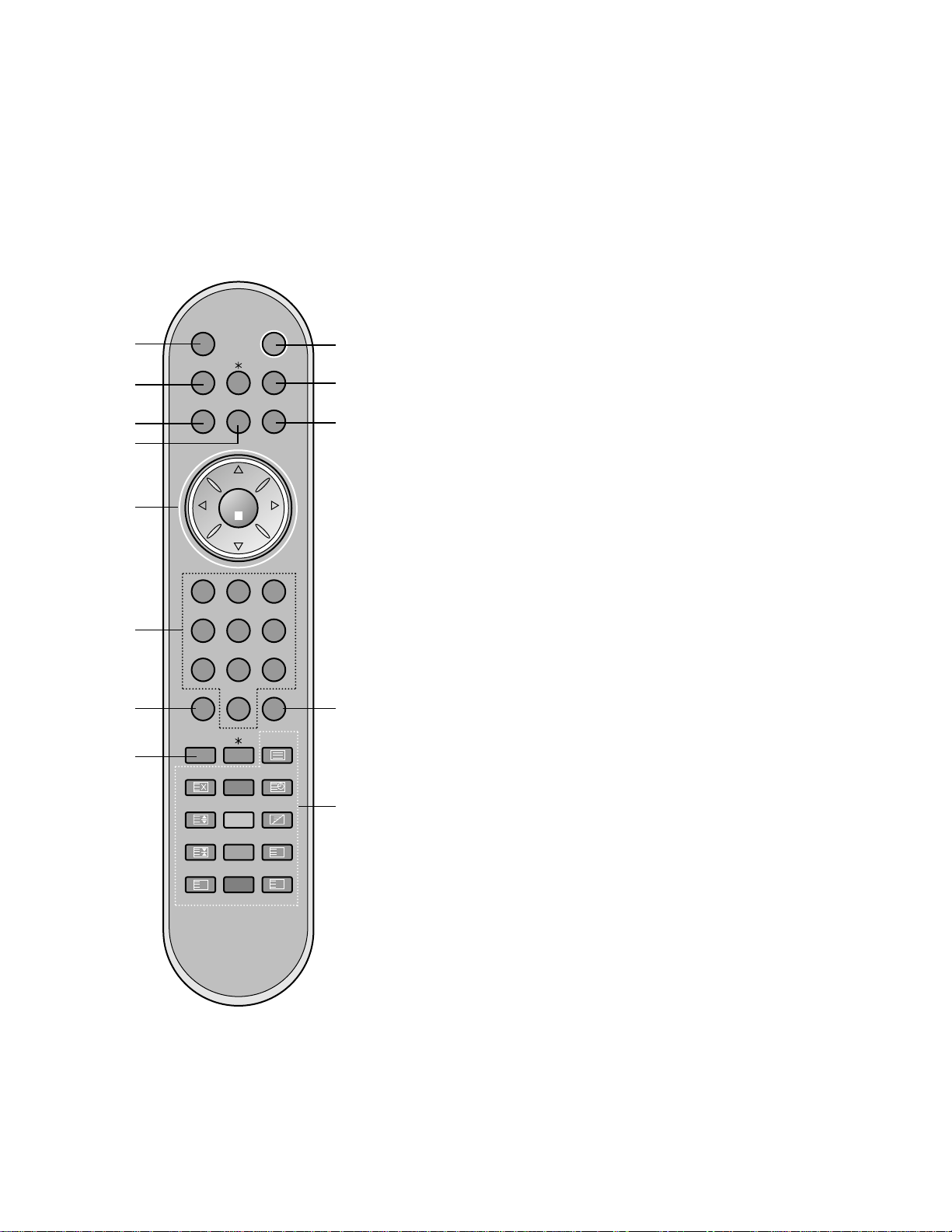
DESCRIPTION OF CONTROLS
- 4 -
POWERMUTE
TV/AV I/II
LIST
PR
PR
VOL
OK
123
456
789
SSM PSM
0
VOL
Q.VIEW MENU
SLEEP TEXT
UPDATE
TIME
SIZE MIX
HOLD
REVEAL
INDEX MODE
?
i
M
RZ model
1
2
3
4
5
6
7
8
All the functions can be controlled with the remote control handset.
Some functions can also be adjusted with the buttons on the side
panel of the set.
Remote control handset
Before you use the remote control handset, please install the batteries. See the next page.
9
1. MUTE
10
11
12
switches the sound on or off.
2. TV/AV
selects TV or AV mode.
clears the menu from the screen.
switches the set on from standby.
3. LIST
displays the programme table.
4. Q.VIEW
returns to the previously viewed programme.
5.
(Programme Up/Down)
DD / EE
selects a programme or a menu item.
switches the set on from standby.
FF / GG (Volume Up/Down)
adjusts the volume.
adjusts menu settings.
OK
accepts your selection or displays the current mode.
6. NUMBER BUTTONS
13
switches the set on from standby and selects a programme.
7. SSM (Sound Status Memory)
recalls your preferred sound setting.
8. SLEEP
sets the sleep timer.
Page 5
- 5 -
POWERMUTE
TV/AV I/II
LIST
PR
PR
VOL
OK
123
456
789
SSM PSM
0
VOL
Q.VIEW MENU
SLEEP TEXT
UPDATE
TIME
SIZE MIX
HOLD
REVEAL
INDEX MODE
?
i
M
RZ model
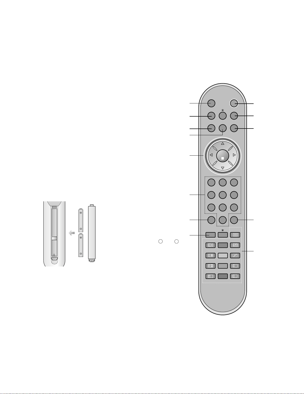
9. POWER
switches the set on from standby or off to standby.
10. I/II
selects the language during dual language broadcast.
selects the sound output (option).
11. MENU
selects a menu.
12. PSM (Picture Status Memory)
recalls your preferred picture setting.
1
2
9
10
13. TELETEXT BUTTONS (option)
These buttons are used for teletext.
For further details, see the ‘Teletext’ section.
: No function
*
COLOURED BUTTONS
These buttons are used for teletext (only TELETEXT models) or
programme edit.
Battery installation
The remote control handset is powered by two AAA/Alkaline type batteries. To load the batteries, turn
the remote control handset over
and open the battery compartment.
Install two batteries as indicated by
the polarity symbols ( and )
marked inside the compartment.
3
11
4
5
6
7
12
8
+
-
13
Note : To avoid damage from possible battery leakage, remove the
batteries if you do not plan to use the remote control handset for an
extended period of time.
Page 6
- 6 -
POWERMUTE
TV/AV
MULTIMEDIA
I/II
LIST
PR
PR
VOL
123
456
789
SSM PSM
0
VOL
EXIT MENU
SLEEP TEXT
UPDATE
TIME
SIZE MIX
HOLD
REVEAL
INDEX MODE
?
i
M
Q.VIEW
OK
RT model
1
2
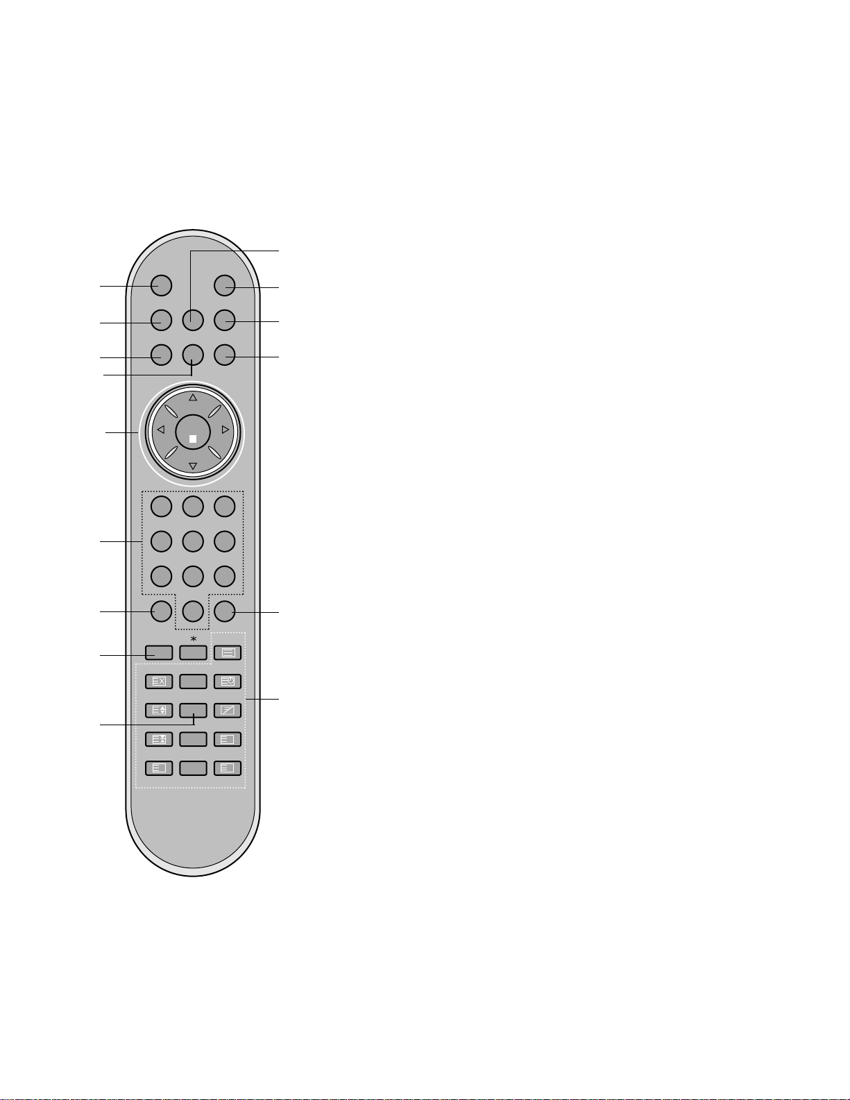
All the functions can be controlled with the remote control handset.
Some functions can also be adjusted with the buttons on the side
panel of the set.
Remote control handset
10
Before you use the remote control handset, please install the batteries. See the next page.
11
1. MUTE
12
switches the sound on or off.
3
4
5
6
7
8
9
13
2. TV/AV
selects the remote operating mode.
clears the menu from the screen.
switches the set on from standby.
3. LIST
displays the programme table.
4. EXIT
clear all on-screen displays and returns to TV viewing from any
menu.
5.
(Programme Up/Down)
DD / EE
selects a programme or a menu item.
switches the set on from standby.
14
FF / GG (Volume Up/Down)
adjusts the volume.
adjusts menu settings.
OK
accepts your selection or displays the current mode.
15
6. NUMBER BUTTONS
switches the set on from standby and selects a programme.
(With TELETEXT)
7. SSM (Sound Status Memory)
recalls your preferred sound setting.
8. SLEEP
sets the sleep timer.
9. Q.VIEW
returns to the previously viewed programme.
Page 7
- 7 -
POWERMUTE
TV/AV
MULTIMEDIA
I/II
LIST
PR
PR
VOL
123
456
789
SSM PSM
0
VOL
EXIT MENU
SLEEP
Q.VIEW
OK
RT model
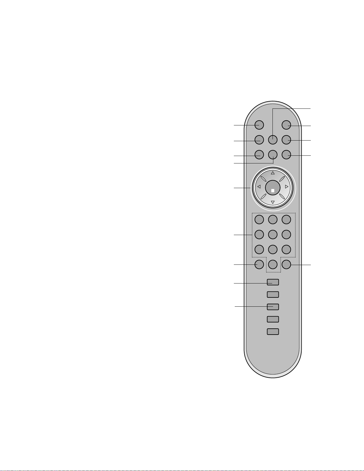
10. MULTIMEDIA
11. POWER
selects TV or Component mode.
switches the set on from standby.
switches the set on from standby or off to standby.
12 I/II
13 MENU
14 PSM (Picture Status Memory)
15 TELETEXT BUTTONS (option)
: No function
*
COLOURED BUTTONS
These buttons are used for teletext (only TELETEXT models) or
programme edit.
selects the language during dual language broadcast.
selects the sound output (option).
selects a menu.
recalls your preferred picture setting.
These buttons are used for teletext.
For further details, see the ‘Teletext’ section.
10
1
2
3
11
12
13
4
5
6
7
14
8
9
(Without TELETEXT)
Page 8
- 8 -
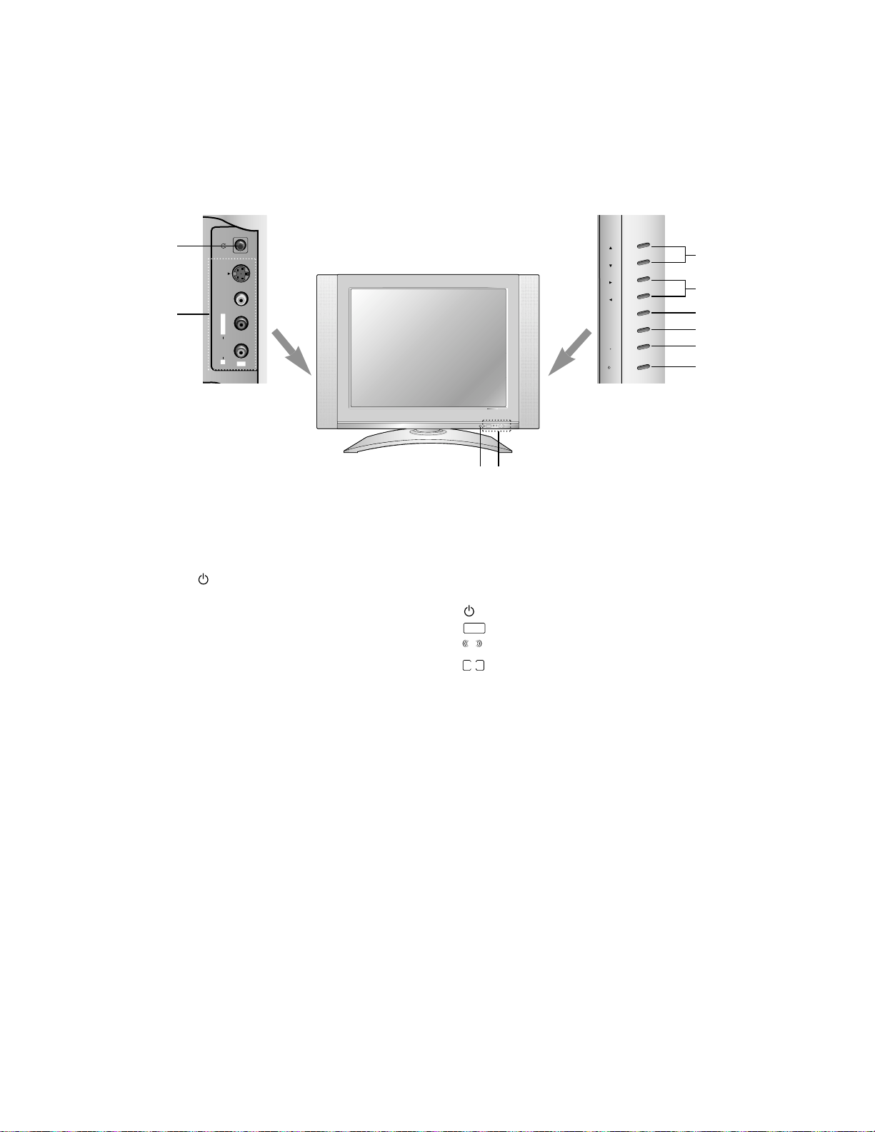
Side panel
MONO
STEREO
ST
DUAL
S-VIDEO VIDEO
AUDIO
R
AV3
L / MONO
PR
VOL
MENU
OK
ON/OFF
TV
AV
/ I
MONO
STEREO
ST
DUAL
9
10
1. ON/OFF ( /I)
switches the set on from standby or off to
standby.
2. TV/AV
selects TV or AV mode.
clears the menu from the screen.
switches the set on from standby.
3. MENU
selects a menu.
4. OK
accepts your selection or displays the current
mode.
5. FF / GG (Volume Up/Down)
adjusts the volume.
adjusts menu settings.
6.
(Programme Up/Down)
DD / EE
selects a programme or a menu item.
switches the set on from standby.
6
5
4
3
2
1
7 8
8. LED (Light Emitting Diode) DISPLAY
illuminates brightly when the set is switched on.
: POWER/STANDBY indicator
: MONO indicator
: STEREO indicator
: DUAL indicator
9. HEADPHONE SOCKET
Connect the headphone plug to this socket.
10. AUDIO/VIDEO IN SOCKETS (AV3)
Connect the audio/video out sockets of external equipment to these sockets.
S-VIDEO/AUDIO IN SOCKETS (S-Video)
Connect the video out socket of an S-VIDEO
VCR to the S-VIDEO socket.
Connects the audio out sockets of the SVIDEO VCR to the audio sockets as in AV3.
7. REMOTE CONTROL SENSOR
Page 9
- 9 -
1. Application range
This specification is applied to ML-012B/C chassis.
2. Requirement for Test
Testing for standard of each part must be followed in below
condition.
(1) Temperature: 25°C ± 5°C(But, CST must be tested 40°C ±
2°C (Humidity: 50%))
(2) Humidity: 65% ± 10%
(3) Power: Standard input voltage (AC 100-220V, 50/60Hz)
(4) Measurement must be performed after heat-run more than
15min.
(5) Adjusting standard for this chassis is followed a special
standard.
3. Test and Inspection method
(1) Capacity: Follow LG electronics TV Testing Standard.
(2) Another Required Standard
Follow the standard of each nation.
SPECIFICATION
NOTE : Specifications and others are subject to change without notice for improvement
.
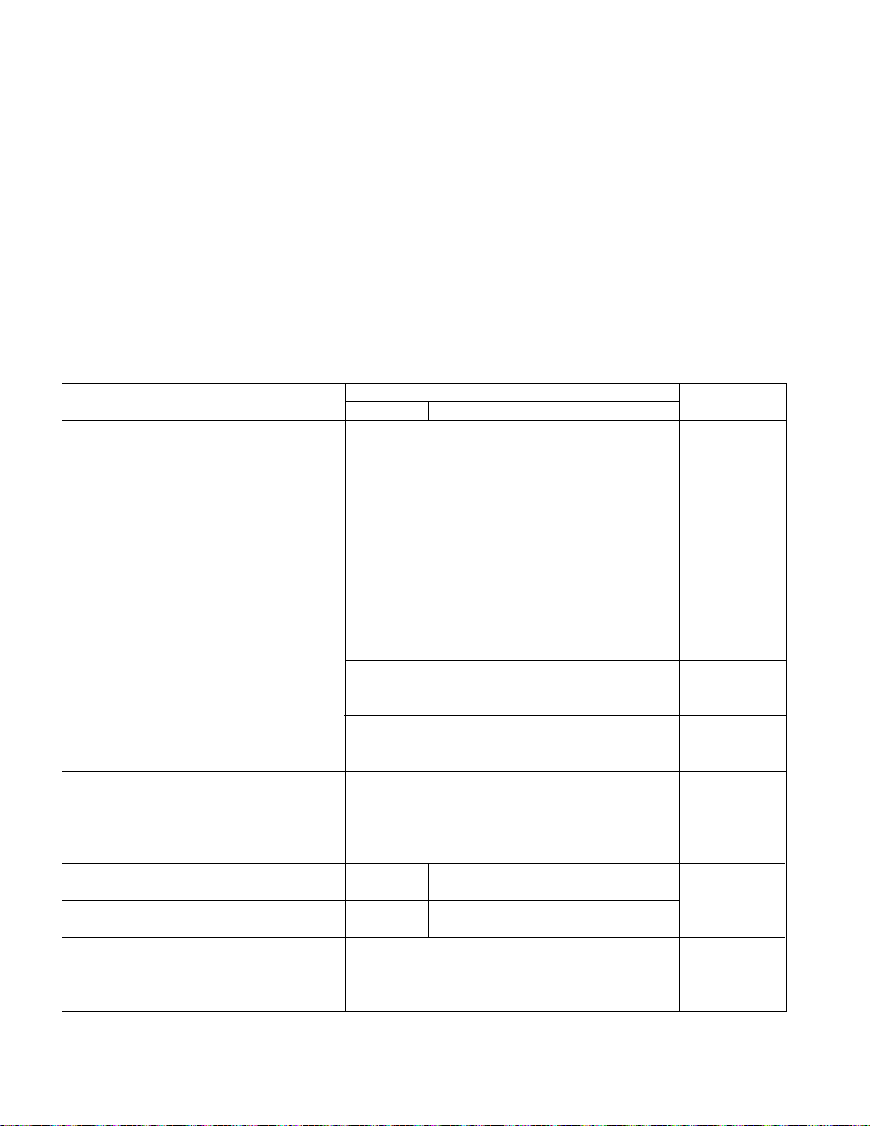
4.General Specification
1
2
3
4
5
6
7
8
9
10
11
Receivable broadcasting system
RF input channel
Input voltage
Tuning system
Picture size
Operating temperature
Operating humidity
Storage temperature
Storage humidity
Display
D4 Jack
Specification
Min Typ Max Unit
1)PAL/SECAM-BG
2)PAL/SECAM-DK
3)PAL-I/I
4)SECAM-L/L’
5)NTSC -M
6)NTSC 4.43(AV)
7)PAL N/M
8)NTSC-M
VHF: E02 ~ E12
UHF : E21 ~ E69
CATV : S1 ~ S20
HYPER : S21 ~ S41
L/L’ : B,C,D
VHF : 2 ~13
UHF : 14 ~ 69
CATV : 1 ~ 125
HYPER : S21 ~S41
V/UHF : 1 ~ 62
CATV : C13 ~ C38
AC 110 - 220V ± 10%, 50/60Hz
AC 230 - 240V/50Hz,AC 100V 50/60Hz
FVS 100 program
FS
38.4cm
0 40 deg
20 80 %
-20 50 deg
30 85 %
LCD Module
1:Y, 3:Pb, 5:Pr, 7:Line1 Ready, 9:LINE2, 11:LINE3, 13:Line3 Ready
2:Y GND, 4:Pb GND, 6:Pr GND, 8:LINE1, 10:Line2 Ready,
12:SWITCH GND, 14:SWITCH
Item Remark
No.
EU/Non-EU
(PAL Market)
NTSC Market
PAL
FRANCE
NTSC
JAPAN
PAL, 200PR.(option)
NTSC
20.1”
LG-PHILPS
Page 10
- 10 -
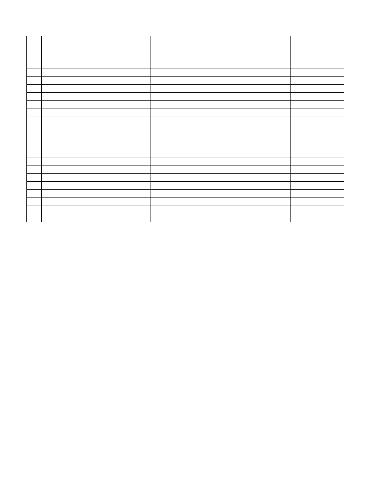
5. Feature and Function
1
2
3
4
5
6
7
8
9
10
11
12
13
14
15
16
17
18
19
20
Teletext
REMOCON
AV input
S-AV input
Component input
PERI TV Connector
RGB input
D-Sub Audio input
2 Carrier stereo
NICAM stereo
2 Carrier dual
NICAM dual
SSC(split screen) mode
MUP(Multi Picture Display) mode
Film mode
Noise reduction
Progressive scan
Motion detection
Dolby virtual
Swivel speaker
TOP,FLOF,LIST 10 page
RC-5 /NEC code(NTSC)
1
1
1
Full SCART : 1
1
1
BG, DK
BG, I, LL’
BG, DK
BG, I, LL’
X
X
X
O
O
X
O
X
Item Specification Remark
No.
TOP(option)
PAL/NTSC
Side & Rear
Side
Rear(option)
Rear(option,EU)
D-Sub 15 pin
(15 inch only)
Stereo(15 Inch only)
Page 11

- 11 -
1. Application Object
This instruction is for the application to the LCD TV.
2. Notes
(1) This set uses an adapter, so connect the adapter and the
set correctly before adjustment.
(2) The adjustment must be performed under the correct
sequence.
(3) The adjustment must be performed in the circumstance of
25!5cC of temperature and 65!10% of relative humidity if
there is no specific designation.
(4) The input voltage of the receiver must keep 100~220V,
50/60Hz in adjusting.
(5) The set must be operated for 30 minutes preliminarily
before adjustment if there is no specific designation.
[ ‘Heat Run’ must be performed with the full white signal or TV
noise signal in the internal part of the set.
[ The time for ‘Heat Run’ can be changed owing to production
plan.
3. Component input mode adjustment
3-1. Required Test Equipment
(1) A pattern generator being in proportion to MSPG925LTH
(or 801F,SETTOP box)
(2) Adjustment Remote controller (SVC Remocon)
3-2. Preparation for Adjustment
(1) Perfome ‘Heat-run’ for more than 20 minutes in the White
Pattern.
(2) Connect the signal of Pattern generator with component
input Jack(YP
bPr
) of LCD TV.
3-3. YPbPrAdjustment
(1) Apply the DTV 1080i,color bar pattern by using
MSPG925LTH. Or apply DTV 1080i color bar pattern of
Pattern generator.
(2) In SVC menu mode,operate YP
bPr
adjustment by using
Volume + button.
ADJUSTMENT INSTRUCTION
Page 12
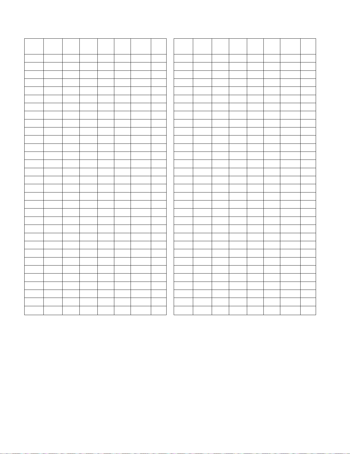
4. Option1 data(200PR~A2 ST:1bit,SYS:2bit)
- 12 -
OPTION
Data
200PR
TEXT
I/II SV
TOP
A2 ST SYS
0
1
2
3
4
5
6
7
8
9
10
11
12
13
14
15
16
17
18
19
20
21
22
23
24
25
26
27
28
29
30
31
0
0
0
0
0
0
0
0
0
0
0
0
0
0
0
0
0
0
0
0
0
0
0
0
0
0
0
0
0
0
0
0
0
0
0
0
0
0
0
0
0
0
0
0
0
0
0
0
0
0
0
0
0
0
0
0
0
0
0
0
0
0
0
0
0
0
0
0
0
0
0
0
0
0
0
0
0
0
0
0
0
0
0
0
0
0
0
0
0
0
0
0
0
0
0
0
0
0
0
0
0
0
0
0
0
0
0
0
0
0
0
0
1
1
1
1
1
1
1
1
1
1
1
1
1
1
1
1
0
0
0
0
1
1
1
1
0
0
0
0
1
1
1
1
0
0
0
0
1
1
1
1
0
0
0
0
1
1
1
1
0
1
2
3
0
1
2
3
0
1
2
3
0
1
2
3
0
1
2
3
0
1
2
3
0
1
2
3
0
1
2
3
SCART
0
0
0
0
0
0
0
0
1
1
1
1
1
1
1
1
0
0
0
0
0
0
0
0
1
1
1
1
1
1
1
1
OPTION
Data
200PR
TEXT
I/II SV
TOP
A2 ST SYS
32
33
34
35
36
37
38
39
40
41
42
43
44
45
46
47
48
49
50
51
52
53
54
55
56
57
58
59
60
61
62
63
0
0
0
0
0
0
0
0
0
0
0
0
0
0
0
0
0
0
0
0
0
0
0
0
0
0
0
0
0
0
0
0
0
0
0
0
0
0
0
0
0
0
0
0
0
0
0
0
0
0
0
0
0
0
0
0
0
0
0
0
0
0
0
0
1
1
1
1
1
1
1
1
1
1
1
1
1
1
1
1
1
1
1
1
1
1
1
1
1
1
1
1
1
1
1
1
0
0
0
0
0
0
0
0
0
0
0
0
0
0
0
0
1
1
1
1
1
1
1
1
1
1
1
1
1
1
1
1
0
0
0
0
1
1
1
1
0
0
0
0
1
1
1
1
0
0
0
0
1
1
1
1
0
0
0
0
1
1
1
1
0
1
2
3
0
1
2
3
0
1
2
3
0
1
2
3
0
1
2
3
0
1
2
3
0
1
2
3
0
1
2
3
SCART
0
0
0
0
0
0
0
0
1
1
1
1
1
1
1
1
0
0
0
0
0
0
0
0
1
1
1
1
1
1
1
1
Page 13
- 13 -
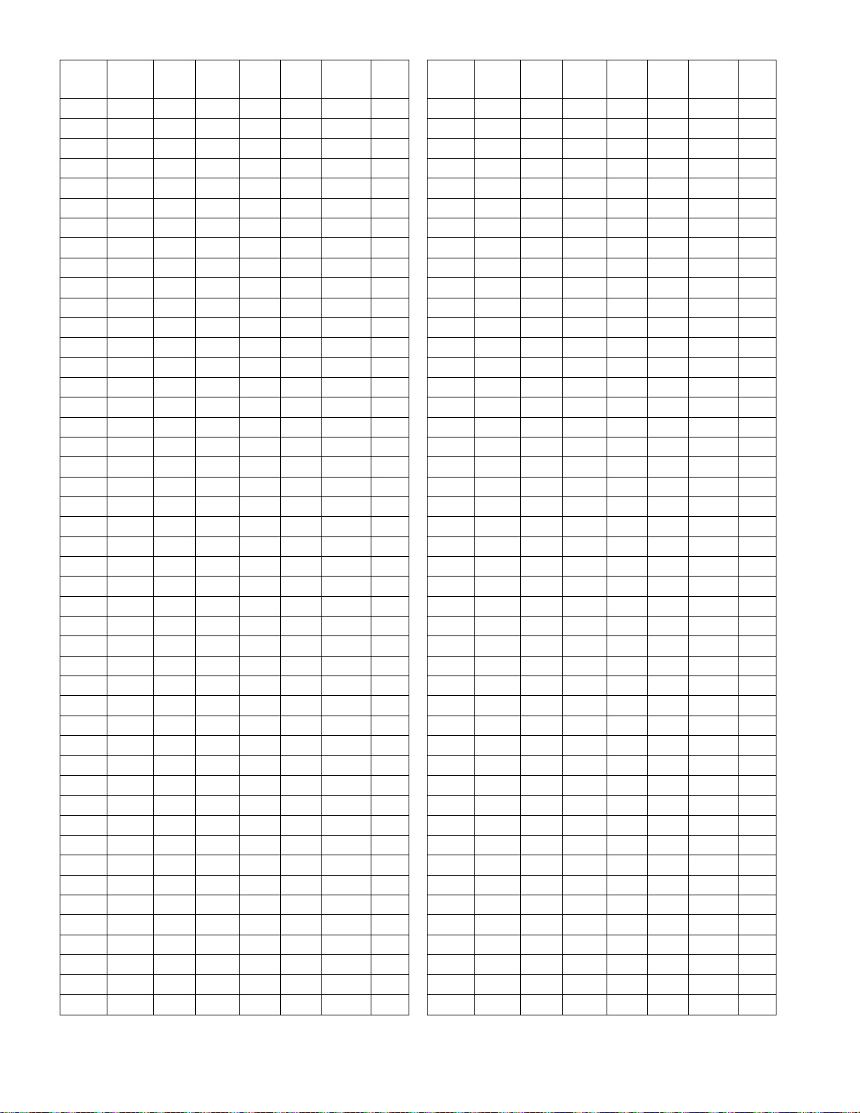
OPTION
Data
200PR
TEXT
I/II SV
TOP
A2 ST SYS
64
65
66
67
68
69
70
71
72
73
74
75
76
77
78
79
80
81
82
83
84
85
86
87
88
89
90
91
92
93
94
95
96
97
98
99
100
101
102
103
104
105
106
107
108
109
0
0
0
0
0
0
0
0
0
0
0
0
0
0
0
0
0
0
0
0
0
0
0
0
0
0
0
0
0
0
0
0
0
0
0
0
0
0
0
0
0
0
0
0
0
0
1
1
1
1
1
1
1
1
1
1
1
1
1
1
1
1
1
1
1
1
1
1
1
1
1
1
1
1
1
1
1
1
1
1
1
1
1
1
1
1
1
1
1
1
1
1
0
0
0
0
0
0
0
0
0
0
0
0
0
0
0
0
0
0
0
0
0
0
0
0
0
0
0
0
0
0
0
0
1
1
1
1
1
1
1
1
1
1
1
1
1
1
0
0
0
0
0
0
0
0
0
0
0
0
0
0
0
0
1
1
1
1
1
1
1
1
1
1
1
1
1
1
1
1
0
0
0
0
0
0
0
0
0
0
0
0
0
0
0
0
0
0
1
1
1
1
0
0
0
0
1
1
1
1
0
0
0
0
1
1
1
1
0
0
0
0
1
1
1
1
0
0
0
0
1
1
1
1
0
0
0
0
1
1
0
1
2
3
0
1
2
3
0
1
2
3
0
1
2
3
0
1
2
3
0
1
2
3
0
1
2
3
0
1
2
3
0
1
2
3
0
1
2
3
0
1
2
3
0
1
SCART
0
0
0
0
0
0
0
0
1
1
1
1
1
1
1
1
0
0
0
0
0
0
0
0
1
1
1
1
1
1
1
1
0
0
0
0
0
0
0
0
1
1
1
1
1
1
OPTION
Data
200PR
TEXT
I/II SV
TOP
A2 ST SYS
110
111
112
113
114
115
116
117
118
119
120
121
122
123
124
125
126
127
128
129
130
131
132
133
134
135
136
137
138
139
140
141
142
143
144
145
146
147
148
149
150
151
152
153
154
155
0
0
0
0
0
0
0
0
0
0
0
0
0
0
0
0
0
0
1
1
1
1
1
1
1
1
1
1
1
1
1
1
1
1
1
1
1
1
1
1
1
1
1
1
1
1
1
1
1
1
1
1
1
1
1
1
1
1
1
1
1
1
1
1
0
0
0
0
0
0
0
0
0
0
0
0
0
0
0
0
0
0
0
0
0
0
0
0
0
0
0
0
1
1
1
1
1
1
1
1
1
1
1
1
1
1
1
1
1
1
0
0
0
0
0
0
0
0
0
0
0
0
0
0
0
0
0
0
0
0
0
0
0
0
0
0
0
0
0
0
1
1
1
1
1
1
1
1
1
1
1
1
1
1
1
1
0
0
0
0
0
0
0
0
0
0
0
0
0
0
0
0
1
1
1
1
1
1
1
1
1
1
1
1
1
1
0
0
0
0
1
1
1
1
0
0
0
0
1
1
1
1
0
0
0
0
1
1
1
1
0
0
0
0
1
1
1
1
0
0
0
0
1
1
1
1
0
0
0
0
2
3
0
1
2
3
0
1
2
3
0
1
2
3
0
1
2
3
0
1
2
3
0
1
2
3
0
1
2
3
0
1
2
3
0
1
2
3
0
1
2
3
0
1
2
3
SCART
1
1
0
0
0
0
0
0
0
0
1
1
1
1
1
1
1
1
0
0
0
0
0
0
0
0
1
1
1
1
1
1
1
1
0
0
0
0
0
0
0
0
1
1
1
1
Page 14
- 14 -
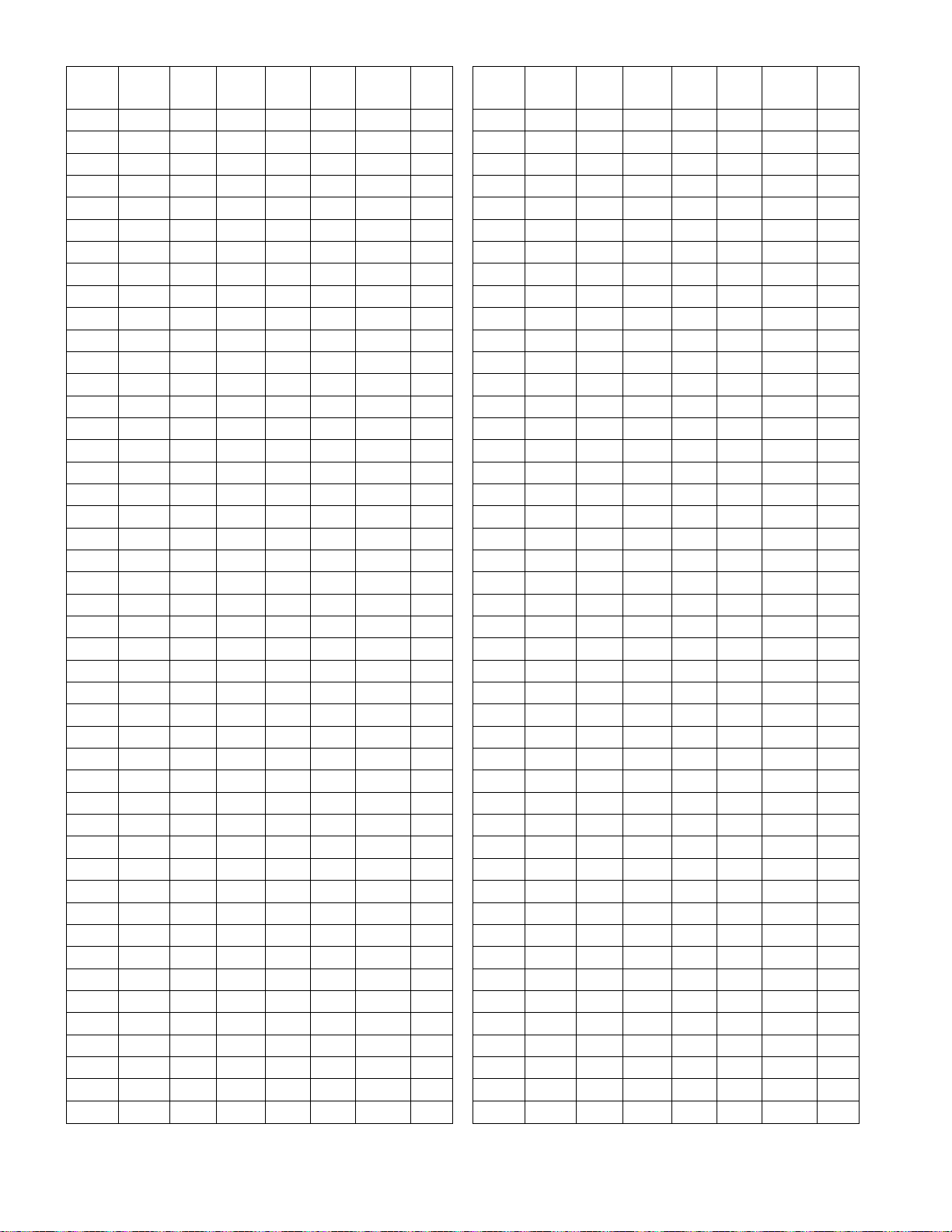
OPTION
Data
200PR
TEXT
I/II SV
TOP
A2 ST SYS
156
157
158
159
160
161
162
163
164
165
166
167
168
169
170
171
172
173
174
175
176
177
178
179
180
181
182
183
184
185
186
187
188
189
190
191
192
193
194
195
196
197
198
199
200
201
1
1
1
1
1
1
1
1
1
1
1
1
1
1
1
1
1
1
1
1
1
1
1
1
1
1
1
1
1
1
1
1
1
1
1
1
1
1
1
1
1
1
1
1
1
1
0
0
0
0
0
0
0
0
0
0
0
0
0
0
0
0
0
0
0
0
0
0
0
0
0
0
0
0
0
0
0
0
0
0
0
0
1
1
1
1
1
1
1
1
1
1
0
0
0
0
1
1
1
1
1
1
1
1
1
1
1
1
1
1
1
1
1
1
1
1
1
1
1
1
1
1
1
1
1
1
1
1
0
0
0
0
0
0
0
0
0
0
1
1
1
1
0
0
0
0
0
0
0
0
0
0
0
0
0
0
0
0
1
1
1
1
1
1
1
1
1
1
1
1
1
1
1
1
0
0
0
0
0
0
0
0
0
0
1
1
1
1
0
0
0
0
1
1
1
1
0
0
0
0
1
1
1
1
0
0
0
0
1
1
1
1
0
0
0
0
1
1
1
1
0
0
0
0
1
1
1
1
0
0
0
1
2
3
0
1
2
3
0
1
2
3
0
1
2
3
0
1
2
3
0
1
2
3
0
1
2
3
0
1
2
3
0
1
2
3
0
1
2
3
0
1
2
3
0
1
SCART
1
1
1
1
0
0
0
0
0
0
0
0
1
1
1
1
1
1
1
1
0
0
0
0
0
0
0
0
1
1
1
1
1
1
1
1
0
0
0
0
0
0
0
0
1
1
OPTION
Data
200PR
TEXT
I/II SV
TOP
A2 ST SYS
202
203
204
205
206
207
208
209
210
211
212
213
214
215
216
217
218
219
220
221
222
223
224
225
226
227
228
229
230
231
232
233
234
235
236
237
238
239
240
241
242
243
244
245
246
247
01
1
1
1
1
1
1
1
1
1
1
1
1
1
1
1
1
1
1
1
1
1
1
1
1
1
1
1
1
1
1
1
1
1
1
1
1
1
1
1
1
1
1
1
1
1
1
1
1
1
1
1
1
1
1
1
1
1
1
1
1
1
1
1
1
1
1
1
1
1
1
1
1
1
1
1
1
1
1
1
1
1
1
1
1
1
1
1
1
1
1
1
0
0
0
0
0
0
0
0
0
0
0
0
0
0
0
0
0
0
0
0
0
0
1
1
1
1
1
1
1
1
1
1
1
1
1
1
1
1
1
1
1
1
1
1
1
1
0
0
0
0
0
0
1
1
1
1
1
1
1
1
1
1
1
1
1
1
1
1
0
0
0
0
0
0
0
0
0
0
0
0
0
0
0
0
1
1
1
1
1
1
1
1
0
0
1
1
1
1
0
0
0
0
1
1
1
1
0
0
0
0
1
1
1
1
0
0
0
0
1
1
1
1
0
0
0
0
1
1
1
1
0
0
0
0
1
1
1
1
2
3
0
1
2
3
0
1
2
3
0
1
2
3
0
1
2
3
0
1
2
3
0
1
2
3
0
1
2
3
0
1
2
3
0
1
2
3
0
1
2
3
0
1
2
3
SCART
1
1
1
1
1
1
0
0
0
0
0
0
0
0
1
1
1
1
1
1
1
1
0
0
0
0
0
0
0
0
1
1
1
1
1
1
1
1
0
0
0
0
0
0
0
0
Page 15
- 15 -
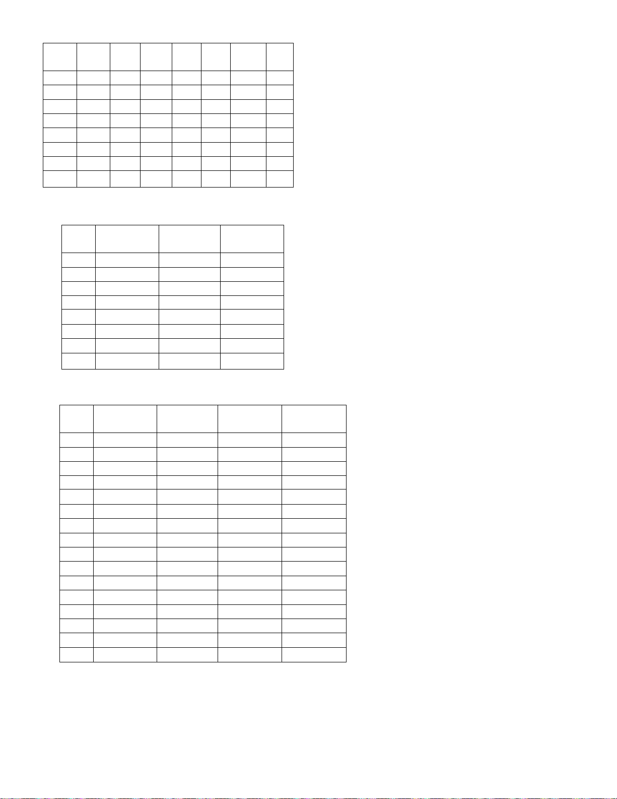
OPTION
Data
200PR
TEXT
I/II SV
TOP
A2 ST SYS
248
249
250
251
252
253
254
255
1
1
1
1
1
1
1
1
1
1
1
1
1
1
1
1
1
1
1
1
1
1
1
1
1
1
1
1
1
1
1
1
0
0
0
0
1
1
1
1
0
1
2
3
0
1
2
3
SCART
1
1
1
1
1
1
1
1
5. Option2 data(ACMS~BBACK:1bit,LANG:3bit)
6. Option3 data(IIC AFT~CH+AU:1bit)
OPTION
Data
ACMS
VOL
0
1
2
3
4
5
6
7
0
0
0
0
1
1
1
1
0
0
1
1
0
0
1
1
HIDEV
0
1
0
1
0
1
0
1
OPTION
Data
IIC AFT
MD SAVE
0
1
2
3
4
5
6
7
8
9
10
11
12
13
14
15
0
0
0
0
0
0
0
0
1
1
1
1
1
1
1
1
0
0
0
0
1
1
1
1
0
0
0
0
1
1
1
1
MONO CH+AUS
0
0
1
1
0
0
1
1
0
0
1
1
0
0
1
1
0
1
0
1
0
1
0
1
0
1
0
1
0
1
0
1
Page 16
- 16 -
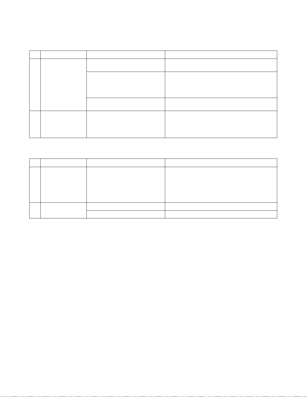
8 No sound Defective Reset IC of IC603 1) Check volume and speaker
- Speaker Defective MSP3421 of IC601 - Sound comes out only when being inputted into Audio
- Earphone Defective B+(8V,5V) of IC604,605. L/R
2) Check after replacing IC603
3) Replace IC601
4) Check and replace B+ of IC604,605.
9 Video color beat noise Earphone shield case being touched
Check the mould of shield and JA2000, Replace shield case
Soldering IC301 and IC912 Re-soldering
1 No screen Input error of inverter connector 1) Bend the pin legs of P1 connector -> recheck them
2) Check and repair the IC804 SI4963,805 SI4925
Pin 40 connector 1) Check and fix P701 connector
being slipped out 2) Check and fix the components at P701 LCD module
and at main board.
3) Check Pin40.
Cracked components and 1) Check and repair tuner board and main board
soldering at tuner board 2) Solder 102.
2 Dark screen 1) Defective LCD lamp 1) Replace the inverter
2) Defective inverter 2) Replace the LCD lamp
3) Input error of inverter connector 2) Check the connector input.
TROUBLESHOOTING
1. General Features
No. Symptom Cause Check Point
Check Point
2. TV and external input
No. Symptom Cause
Page 17
- 17 -
PRINTED CIRCUIT BOARD
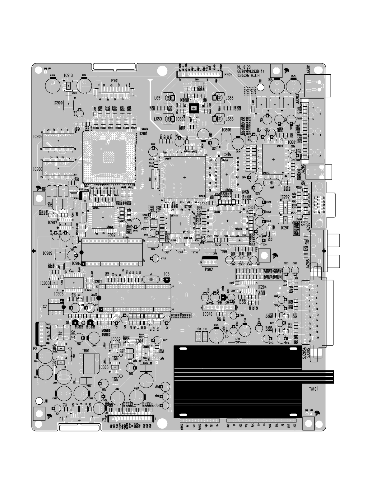
MAIN(TOP)
Page 18
- 18 -
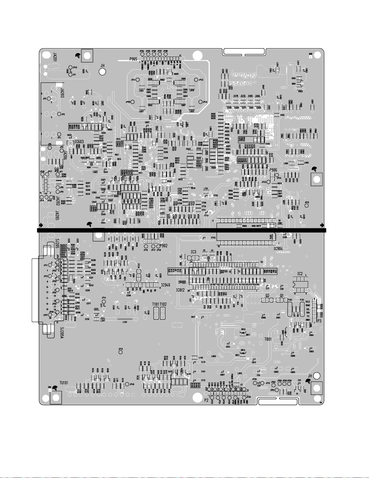
MAIN BOARD(BOTTOM)
Page 19
- 19 -
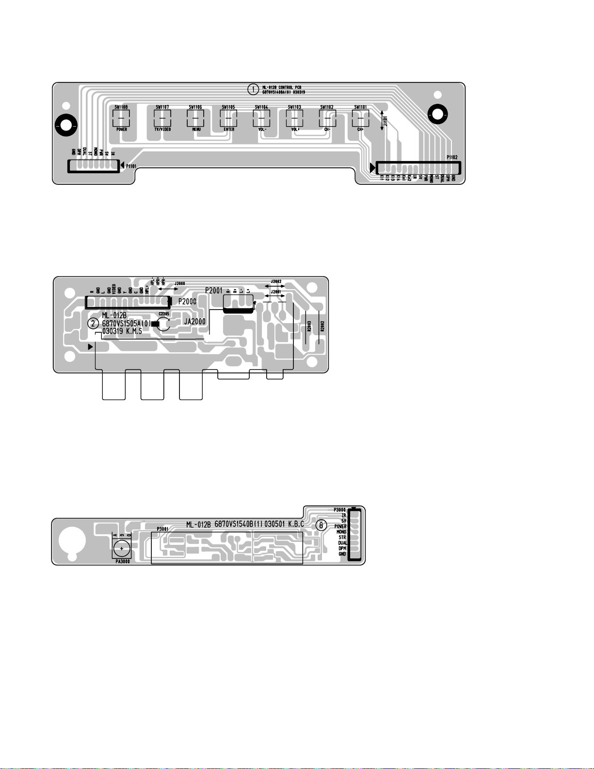
CONTROL BOARD
SIDE AV BOARD
LED BOARD
Page 20
- 20 -
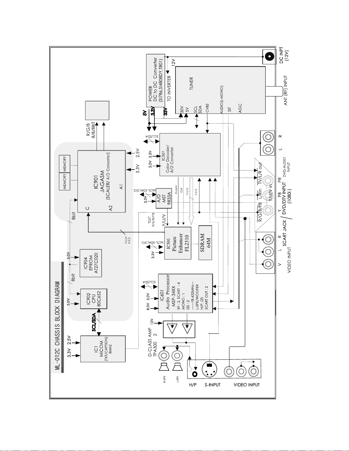
BLOCK DIAGRAM
P701
TTL
VPC3230D
4T
Page 21

MEMO
- 21 -
Page 22
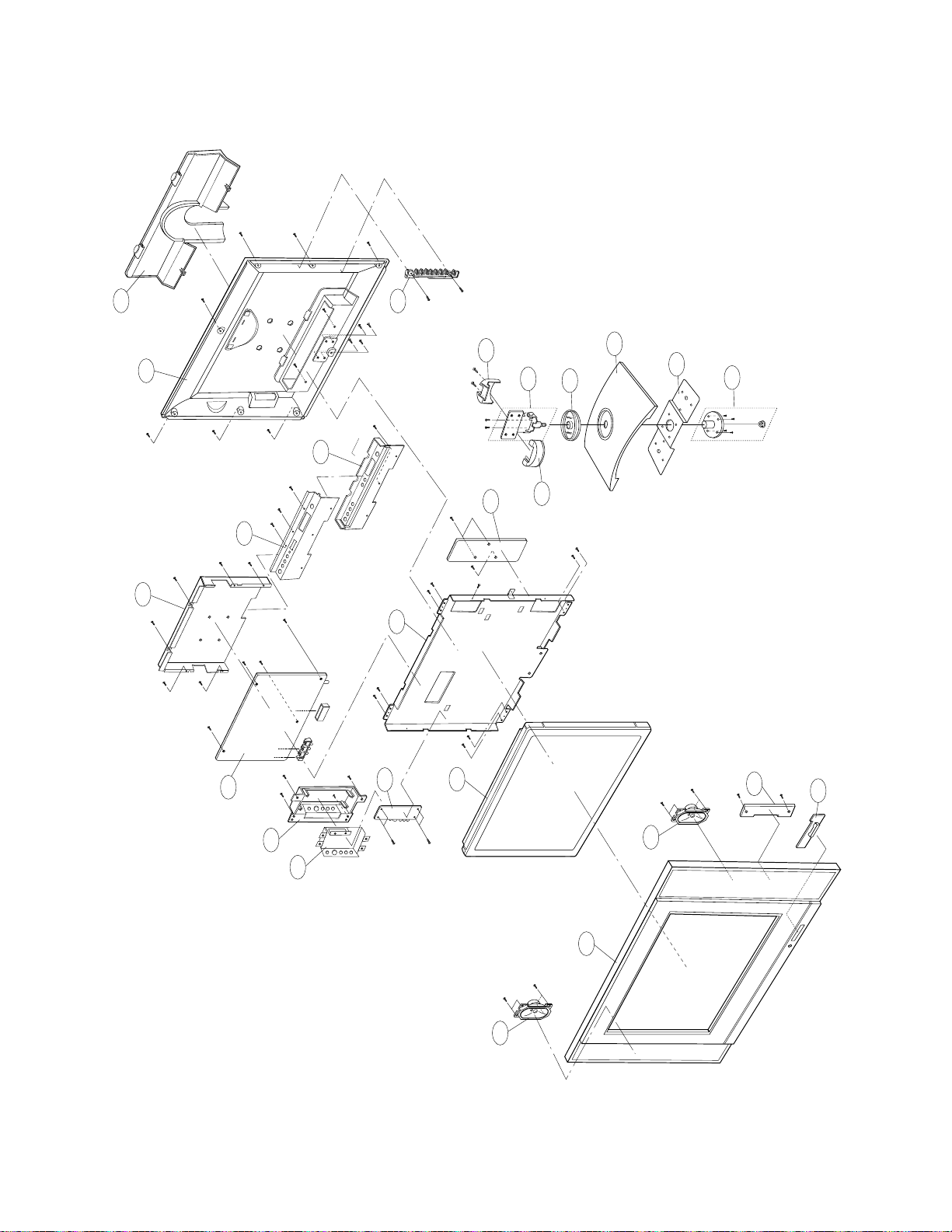
- 22 -
EXPLODED VIEW
430
400
320
210
220
310
250
350
540
330
340
360
370
380
330
520
230
240
550
112
120
300
120
530
560
Page 23

- 23 -
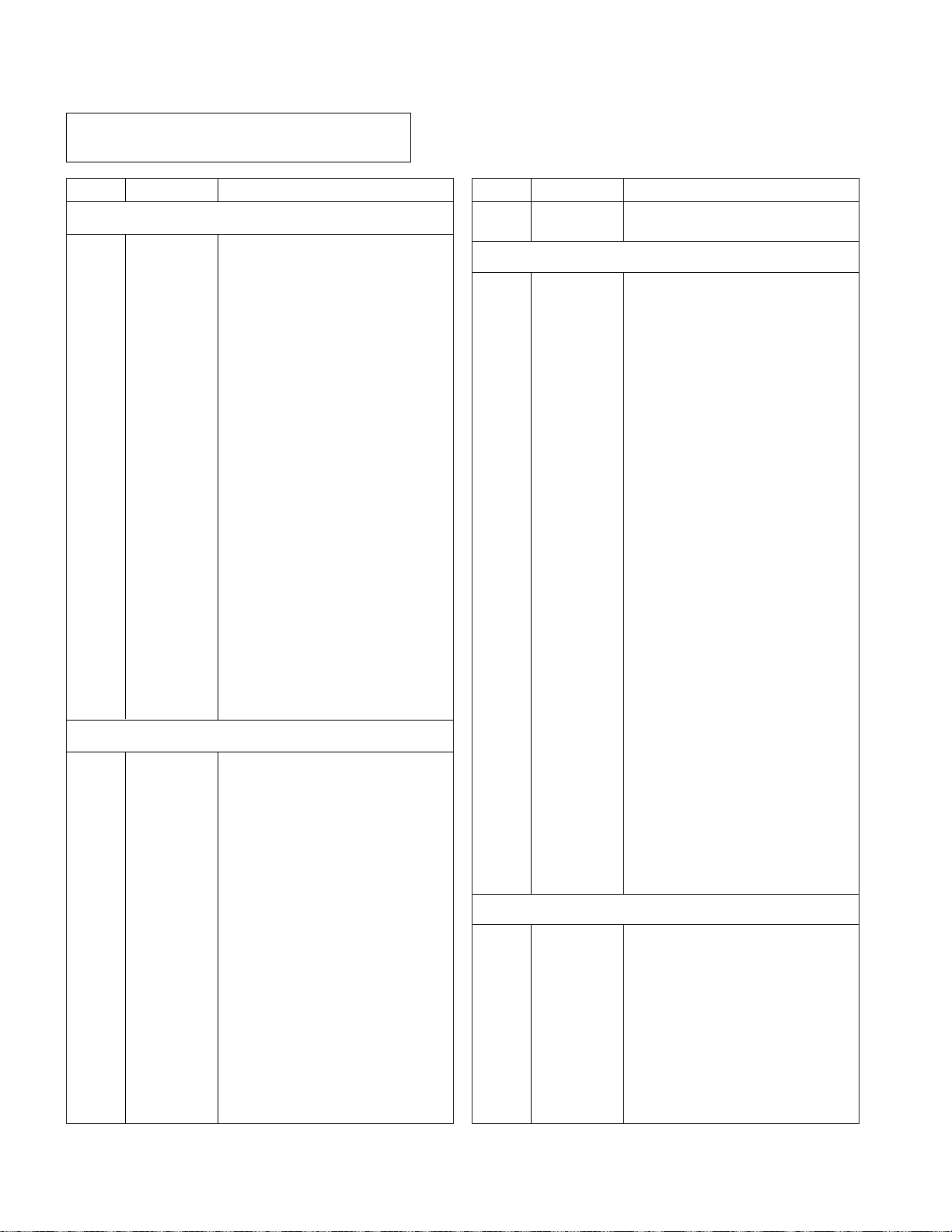
112 6304VT2011B LCD MODULE,LC201V02-A3(IPS) COLOR 20.1” 640*RGB*480 450CD/M2
120 6400GKTX01A SPEAKER,FULLRANGE 8OHM 7/12W 83DB OTHERS 34.5X71
6400GKTX01B SPEAKER,FULLRANGE F1527C-6428-2 K-TONE (RT-, ALPHA)
210 4950V00141A METAL, SHIELD NON REAR AV (RT-20LA60, ALPHA)
4950V00141C METAL,BRACKET SBHG .
220 4810V00764F BRACKET,REAR AV RZ-20LA60 ML012B HIPS 407AF
4810V00764K BRACKET,REAR AV RP-20LA60 ML012B HIPS 60HR(ALPHA)
230 4810V00765D BRACKET,SIDE AV 15/20LA60 ML012B HIPS 60HR .
4810V00765J BRACKET,SIDE AV RT-20LA60 ML012B (ALPHA)
240 4950V00142A METAL,SHIELD NON SIDE AV, 20LA60/15LA60
250 4950V00132A METAL,MAIN FRAME NON 20LA60
4950V00132B METAL,FRAME SBHG RZ-20LA60 C/SKD(BN,FS,IS,ES)
300 3091V00491D CABINET ASSEMBLY,RZ-20LA60 STEREO ML012B .
3091V00491G CABINET ASSEMBLY,RZ-20LA60 STEREO ML012B C/SKD(BN,FS,IS,ES)
310 5020V00776B BUTTON,CONTROL RU-20LA60 ABS, HF-380 8KEY .
320 4950V00140B METAL,SHIELD SBHG 20LA60
4950V00140D METAL,COVER SBHG 20LA60
330 4950V00157C METAL,HINGE ASSY SPCC(CR) 20LA60
340 4810V00767B BRACKET,STAND HINGE FRONT RU-20LA60 ML012B ABS, HF-380 .
350 4810V00768B BRACKET,STAND HINGE COVER RU-20LA60 ML012B ABS, HF-380 .
360 4810V00766B BRACKET,DECO STAND RU-20LA60 ML012B ABS, HF-380 .
370 4810V00769B BRACKET,STAND RU-20LA60 ML012B ABS, HF-380 BASE
380 4950V00133B METAL,BASE SPCC(CR) .
400 3809V00339E BACK COVER ASSEMBLY,1SCART 3850VC0002G(LGEAK,KIEV,LGERU)
3809V00339H BACK COVER ASSEMBLY,RT-20LA60 ML012B NON(ALPHA)
3809V00339J BACK COVER ASSEMBLY,RZ-20LA60 1SCART C/SKD(BN,FS,IS,ES)
3809V00339K BACK COVER ASSEMBLY,1SCART 3850VC0002F(V-LUX,LGEPL)
430 3550V00297A COVER,AV COVER 20LA60 NON REAR
520 6871VMMP85B PWB(PCB) ASSEMBLY,MAIN ML012B RZ-20LA60(LGEPL,V-LUX))
6871VMMP85C PWB(PCB) ASSEMBLY,MAIN ML012B RZ-20LA60(C/SKD)(BN,FS,IS,ES)
6871VMMP85E PWB(PCB) ASSEMBLY,MAIN ML012B RZ-20LA60(CIS-AK,KIEV,RU)
6871VMMQ69B PWB(PCB) ASSEMBLY,MAIN ML012B RT-20LA60(ALPHA)
530 6871VSMV38A PWB(PCB) ASSEMBLY,SUB CONT ML012B RZ-15/20LA60 CONTROL ASSY
540 6633VA0003Q INVERTER ASSEMBLY,15V NON K.S. LC201V02-A3 IPS
550 6871VSMV40D PWB(PCB) ASSEMBLY,SUB A/V ML012B RZ-15/20LA60 SIDE AV ASSY
6871VSMV40G PWB(PCB) ASSEMBLY,SUB A/V ML012B RT-15/20LA60 SIDE AV (ALPHA)
560 6871VSMV43A PWB(PCB) ASSEMBLY,SUB SUB ML012B 20 INDEX LED ASSY
EXPLODED VIEW PARTS LIST
No.
PART NO.
DESCRIPTION
Page 24
REPLACEMENT PARTS LIST
LOCA. NO PART NO DESCRIPTION
ZD82
ZD83
IC802
IC803
IC804
IC805
IC913
Q101
Q102
Q105
Q106
Q107
Q204
Q205
Q206
Q211
Q212
Q213
Q214
Q3
Q3000
Q3001
Q3002
Q3003
Q3004
Q3005
Q301
Q4
Q603
Q604
Q801
Q901
Q902
Q903
Q904
C101
C103
C105
C109
C111
C112
C113
C17
C20
C21
0DZRM00178A
0DZRM00178A
0TFVI80001A
0TFVI80001A
0TFVI80005A
0TF492509AA
0TF492509AA
0TR150400BA
0TR387500AA
0TR387500AA
0TR387500AA
0TR387500AA
0TR387500AA
0TR387500AA
0TR387500AA
0TR387500AA
0TR387500AA
0TR387500AA
0TR387500AA
0TR387500AA
0TR387500AA
0TR387500AA
0TR387500AA
0TR387500AA
0TR387500AA
0TR387500AA
0TR387500AA
0TR387500AA
0TR150400BA
0TR150400BA
0TR387500AA
0TR387500AA
0TR387500AA
0TR387500AA
0TR387500AA
0CE476DH618
0CE106DK618
0CE687DD618
0CE227DF618
0CE105DK618
0CE476DF618
0CE107DF618
0CE107DF618
0CE107DF618
0CE106DF618
DIODE, R/TP SMD 0.2W 5.1V 5MA -PF
DIODE, R/TP SMD 0.2W 5.1V 5MA -PF
TR, R/TP SO-8 30V 7.5A OLD
TR, R/TP SO-8 30V 7.5A OLD
TR, R/TP SO-8 -20V 6.2A
TR, SI4925DY TP TEMIC 30V 6.1A SO-8
TR, SI4925DY TP TEMIC 30V 6.1A SO-8
TR, CHIP 2SA1504S(ASY) KEC
TR, CHIP 2SC3875S(ALY) KEC
TR, CHIP 2SC3875S(ALY) KEC
TR, CHIP 2SC3875S(ALY) KEC
TR, CHIP 2SC3875S(ALY) KEC
TR, CHIP 2SC3875S(ALY) KEC
TR, CHIP 2SC3875S(ALY) KEC
TR, CHIP 2SC3875S(ALY) KEC
TR, CHIP 2SC3875S(ALY) KEC
TR, CHIP 2SC3875S(ALY) KEC
TR, CHIP 2SC3875S(ALY) KEC
TR, CHIP 2SC3875S(ALY) KEC
TR, CHIP 2SC3875S(ALY) KEC
TR, CHIP 2SC3875S(ALY) KEC
TR, CHIP 2SC3875S(ALY) KEC
TR, CHIP 2SC3875S(ALY) KEC
TR, CHIP 2SC3875S(ALY) KEC
TR, CHIP 2SC3875S(ALY) KEC
TR, CHIP 2SC3875S(ALY) KEC
TR, CHIP 2SC3875S(ALY) KEC
TR, CHIP 2SC3875S(ALY) KEC
TR, CHIP 2SA1504S(ASY) KEC
TR, CHIP 2SA1504S(ASY) KEC
TR, CHIP 2SC3875S(ALY) KEC
TR, CHIP 2SC3875S(ALY) KEC
TR, CHIP 2SC3875S(ALY) KEC
TR, CHIP 2SC3875S(ALY) KEC
TR, CHIP 2SC3875S(ALY) KEC
47UF STD 25V 20% FL TP 5
10UF STD 50V M FL TP5
680UF STD 10V 20% FL TP 5
220UF STD 16V M FL TP5
1UF STD 50V M FL TP5
47UF STD 16V M FL TP5
100UF STD 16V M FL TP5
100UF STD 16V M FL TP5
100UF STD 16V M FL TP5
10UF STD 16V M FL TP5
LOCA. NO PART NO DESCRIPTION
IC2
IC204
IC3
IC301
IC501
IC600
IC603
IC604
IC605
IC606
IC701
IC801
IC806
IC900
IC901
IC902
IC903
IC905
IC906
IC907
IC908
IC909
IC915
IC940
Q1
Q2
D1
D2
D801
D802
D811
D812
ZD101
ZD3000
ZD3001
ZD71
ZD72
ZD73
ZD74
ZD75
ZD76
ZD77
ZD79
ZD80
ZD81
0IAL241610B
0IPH860100B
0IFA752700A
0IIT323000E
0IMCRGN001B
0IMCRTI022D
0IKE704200J
0IMCRFA009A
0IMCRFA008A
0IMCRKE010A
0IMCRM3001A
0ITC786000A
0IMCRFA020A
0IMCRKE010A
0IMCRG2004B
0IPH806520A
0IPH743730E
0ISS416162C
0ISS416162C
0IPH740400G
0IMCRAL006A
0IMCRFA020A
0IMMRHY033A
0ISA701600A
0IFA270000A
0IFA270000A
0DD181009AB
0DD181009AB
0DD181009AB
0DD100009AM
0DD414809ED
0DD414809ED
0DZ330009BA
0DZRM00178A
0DZRM00178A
0DZRM00178A
0DZRM00178A
0DZRM00178A
0DZRM00178A
0DZRM00178A
0DZRM00178A
0DZRM00178A
0DZRM00178A
0DZRM00178A
0DZRM00178A
IC, 8PIN DIP ST EEPROM NON
IC, TDA8601T 16P-SOP BK FAST
IC, KA75270Z 3 TP RE-SET IC MC-007
IC, VPC3230D C5 80P QFP TRAY VIDEO
IC, FLI2310BC 208P PQFP TRAY DIGITAL
IC, TPA3004D2 48P PQFP TRAY 9W AUDIO
IC, KIA7042AF SOT-89 TP 4.2V VOLTAGE
IC, KA78M08RTM,2P D-PAK, R/TP
IC, KA78M05RTM,2P D-PAK, R/TP
IC, KIA7812AF KEC 2P DPACK R/TP 12V
IC, MST9883A 80P A/D CONVERTER(RT MODEL)
IC, SI786 28SSOP TP DUAL-OUTPUT
IC, R/TP 2.5V 3A L/DROP REGU.
IC, KIA7812AF KEC 2P DPACK R/TP 12V
IC, JAGASM A4 SAGE 352BALL TRAY
IC, 80C652 40 PLCC ST 8-BIT
IC, 74HCT373 D 20SOP R/TP ADDRESS
IC, 50TSOP R/TP SDRAM 512K*16BIT*2B
IC, 50TSOP R/TP SDRAM 512K*16BIT*2B
IC, 74HC04D HEX INVERTER 14P,SOP TP .
IC, AT24C16AN-10SI-2.7 8P SOIC R/TP EEPROM
IC, RC1587DT_363P TO252 DPAK R/TP 2.5V 3A
IC, 86P TSOP TRAY 64M F/MEMORY
IC, LA7016 8S ANALOG S/W - - - IC, 3P TP LEVEL SHIFT 60V/0.2A,MC007A
IC, 3P TP LEVEL SHIFT 60V/0.2A,MC007A
DIODE, KDS181 TP KEC - 85V - - - 300MA
DIODE, KDS181 TP KEC - 85V - - - 300MA
DIODE, KDS181 TP KEC - 85V - - - 300MA
DIODE, EU1ZV(1) TP SANKEN
DIODE, 1N4148 TP GRANDE - - - - - DIODE, 1N4148 TP GRANDE - - - - - DIODE, ZENER HZT33 TAPING
DIODE, R/TP SMD 0.2W 5.1V 5MA -PF
DIODE, R/TP SMD 0.2W 5.1V 5MA -PF
DIODE, R/TP SMD 0.2W 5.1V 5MA -PF
DIODE, R/TP SMD 0.2W 5.1V 5MA -PF
DIODE, R/TP SMD 0.2W 5.1V 5MA -PF
DIODE, R/TP SMD 0.2W 5.1V 5MA -PF
DIODE, R/TP SMD 0.2W 5.1V 5MA -PF
DIODE, R/TP SMD 0.2W 5.1V 5MA -PF
DIODE, R/TP SMD 0.2W 5.1V 5MA -PF
DIODE, R/TP SMD 0.2W 5.1V 5MA -PF
DIODE, R/TP SMD 0.2W 5.1V 5MA -PF
DIODE, R/TP SMD 0.2W 5.1V 5MA -PF
IC
DIODE
- 2 4 -
TRANSISTOR
CAPACITOR
For Capacitor & Resistors, the
charactors at 2nd and 3rd digit
in the P/No. means as follows;
CC, CX, CK, CN : Ceramic
CQ : Polyestor
CE : Electrolytic
RD : Carbon Film
RS : Metal Oxide Film
RN : Metal Film
RF : Fusible
Page 25
- 2 5 -
LOCA. NO PART NO DESCRIPTION
C214
C216
C217
C220
C221
C222
C223
C2300
C2301
C2302
C2304
C2305
C2306
C2307
C2309
C2310
C24
C25
C281
C290
C291
C292
C319
C323
C323
C327
C334
C335
C336
C344
C347
C348
C349
C353
C354
C361
C361
C362
C362
C363
C363
C364
C364
C365
C406
C418
C493
C494
C495
C527
C532
C610
0CE4763F618
0CE227DD618
0CE476DD618
0CE476DD618
0CE476DD618
0CE226DF618
0CE226DF618
0CH2103K516
0CH2103K516
0CH3104K566
0CH5331K416
0CE225DK618
0CH5331K416
0CH5391K416
0CH5471K416
0CH5471K416
0CE107DF618
0CE227DF618
0CE106DF618
0CE106DK618
0CE107DF618
0CE106DK618
0CE107SF6DC
0CE106DF618
0CE106SF6DC
0CE107DF618
0CK224DF56A
0CK224DF56A
0CK224DF56A
0CE476DF618
0CK224DF56A
0CE226DF618
0CE107DF618
0CE476DF618
0CK224DF56A
0CE105CK636
0CE105DK618
0CE105CK636
0CE105DK618
0CE105CK636
0CE105DK618
0CE105CK636
0CE105DK618
0CK224DF56A
0CE476DF618
0CE107SF6DC
0CE106DF618
0CE107DF618
0CE107DF618
0CE107DF618
0CE107DF618
0CE107DF618
47UF SRE 16V M FL TP5
220UF STD 10V M FL TP5
47UF STD 10V 20% FL TP 5
47UF STD 10V 20% FL TP 5
47UF STD 10V 20% FL TP 5
22UF STD 16V M FL TP5
22UF STD 16V M FL TP5
10000P 50V K B 2.0X1.25 R/TP
10000P 50V K B 2.0X1.25 R/TP
0.1UF 50V 10% X7R 2012 R/TP
330PF 50V J NP0 2012 R/TP
2.2UF STD 50V 20% FL TP 5
330PF 50V J NP0 2012 R/TP
390PF 50V J NP0 2012 R/TP
470PF 50V J NP0 2012 R/TP
470PF 50V J NP0 2012 R/TP
100UF STD 16V M FL TP5
220UF STD 16V M FL TP5
10UF STD 16V M FL TP5
10UF STD 50V M FL TP5
100UF STD 16V M FL TP5
10UF STD 50V M FL TP5
100UF MVG 16V M SMD R/TP
10UF STD 16V M FL TP5
10UF MVG 16V 20% R/TP(SMD) SMD
100UF STD 16V M FL TP5
220000PF 2012 16V 10% R/TP X7R
220000PF 2012 16V 10% R/TP X7R
220000PF 2012 16V 10% R/TP X7R
47UF STD 16V M FL TP5
220000PF 2012 16V 10% R/TP X7R
22UF STD 16V M FL TP5
100UF STD 16V M FL TP5
47UF STD 16V M FL TP5
220000PF 2012 16V 10% R/TP X7R
1UF SHL,SD 50V M FM5 BP(D) TP
1UF STD 50V M FL TP5
1UF SHL,SD 50V M FM5 BP(D) TP
1UF STD 50V M FL TP5
1UF SHL,SD 50V M FM5 BP(D) TP
1UF STD 50V M FL TP5
1UF SHL,SD 50V M FM5 BP(D) TP
1UF STD 50V M FL TP5
220000PF 2012 16V 10% R/TP X7R
47UF STD 16V M FL TP5
100UF MVG 16V M SMD R/TP
10UF STD 16V M FL TP5
100UF STD 16V M FL TP5
100UF STD 16V M FL TP5
100UF STD 16V M FL TP5
100UF STD 16V M FL TP5
100UF STD 16V M FL TP5
LOCA. NO PART NO DESCRIPTION
C614
C618
C619
C620
C621
C622
C631
C632
C633
C635
C638
C639
C640
C641
C642
C643
C656
C658
C659
C662
C669
C670
C671
C672
C673
C676
C677
C680
C681
C682
C683
C685
C712
C719
C733
C734
C742
C801
C802
C803
C804
C805
C806
C807
C808
C814
C815
C817
C825
C826
C836
C837
0CE107DF618
0CK224DF56A
0CK224DF56A
0CK224DF56A
0CK224DF56A
0CE476DF618
0CE106DF618
0CE106DF618
0CE335DK618
0CE107DF618
0CE107DF618
0CE107DF618
0CK224DF56A
0CK224DF56A
0CK224DF56A
0CK224DF56A
0CK105DF64A
0CK105DF64A
0CK105DF64A
0CK105DF64A
0CK105DF64A
0CK105DF64A
0CK105DF64A
0CK105DF64A
0CK105DF64A
0CK224DF56A
0CK224DF56A
0CK224DF56A
0CK224DF56A
0CE227DF618
0CK105DF64A
0CE107DD618
0CE107SF6DC
0CE107SF6DC
0CE107DD618
0CE107SF6DC
0CE107SF6DC
0CE476DK618
0CE477DF618
0CE477DF618
0CE477DF618
0CE477DF618
0CE477DF618
0CE477DF618
0CE227DH618
0CE107DH618
0CE107DH618
0CE475DK618
0CE337DH618
0CE337DH618
0CE227DF618
0CE227DD618
100UF STD 16V M FL TP5
220000PF 2012 16V 10% R/TP X7R
220000PF 2012 16V 10% R/TP X7R
220000PF 2012 16V 10% R/TP X7R
220000PF 2012 16V 10% R/TP X7R
47UF STD 16V M FL TP5
10UF STD 16V M FL TP5
10UF STD 16V M FL TP5
3.3UF STD 50V 20% FL TP 5
100UF STD 16V M FL TP5
100UF STD 16V M FL TP5
100UF STD 16V M FL TP5
220000PF 2012 16V 10% R/TP X7R
220000PF 2012 16V 10% R/TP X7R
220000PF 2012 16V 10% R/TP X7R
220000PF 2012 16V 10% R/TP X7R
1UF 2012 16V 20% R/TP F(Y5V)
1UF 2012 16V 20% R/TP F(Y5V)
1UF 2012 16V 20% R/TP F(Y5V)
1UF 2012 16V 20% R/TP F(Y5V)
1UF 2012 16V 20% R/TP F(Y5V)
1UF 2012 16V 20% R/TP F(Y5V)
1UF 2012 16V 20% R/TP F(Y5V)
1UF 2012 16V 20% R/TP F(Y5V)
1UF 2012 16V 20% R/TP F(Y5V)
220000PF 2012 16V 10% R/TP X7R
220000PF 2012 16V 10% R/TP X7R
220000PF 2012 16V 10% R/TP X7R
220000PF 2012 16V 10% R/TP X7R
220UF STD 16V M FL TP5
1UF 2012 16V 20% R/TP F(Y5V)
100UF STD 10V M FL TP5
100UF MVG 16V M SMD R/TP
100UF MVG 16V M SMD R/TP
100UF STD 10V M FL TP5
100UF MVG 16V M SMD R/TP
100UF MVG 16V M SMD R/TP
47UF STD 50V M FL TP5
470UF STD 16V 20% FL TP 5
470UF STD 16V 20% FL TP 5
470UF STD 16V 20% FL TP 5
470UF STD 16V 20% FL TP 5
470UF STD 16V 20% FL TP 5
470UF STD 16V 20% FL TP 5
220UF STD 25V M FL TP5
100UF STD 25V M FL TP5
100UF STD 25V M FL TP5
4.7UF STD 50V 20% FL TP 5
330UF STD 25V M FL TP5
330UF STD 25V M FL TP5
220UF STD 16V M FL TP5
220UF STD 10V M FL TP5
For Capacitor & Resistors, the
charactors at 2nd and 3rd digit
in the P/No. means as follows;
CC, CX, CK, CN : Ceramic
CQ : Polyestor
CE : Electrolytic
RD : Carbon Film
RS : Metal Oxide Film
RN : Metal Film
RF : Fusible
Page 26
- 2 6 -
LOCA. NO PART NO DESCRIPTION
C902
C904
C906
C911
C915
C935
C953
C954
R2011
JA2000
JA201
JA203
JA205A
JA205B
SJ205
L102
L208
L2102
L2103
L2104
L219
L220
L221
L222
L223
L802
L803
T801
P1101
P1102
P2000
P2001
P3
C2307
R2002
R2003
R2004
R2005
R2006
R2007
R2008
R2009
R2010
R2011
0CE106SF6DC
0CE106SF6DC
0CE107DF618
0CE107SF6DC
0CE106SF6DC
0CE107SF6DC
0CE477DF618
0CE477DF618
0CH5391K416
6613V00018A
6612VAH001C
6613V00004P
380-336E
380-336F
6612M00001A
0LA0272K139
0LC1020101A
0LC0233002A
0LC0233002A
0LC0233002A
0LC0233002A
0LC0233002A
0LC0233002A
0LC0233002A
0LC0233002A
6140VB0004B
6140VB0004A
6170VTCA30A
366-169G
6631V20016G
6631V20016C
366-922C
366-932E
0RH4703D622
0RD1200H609
0RD1200H609
0RH0472D622
0RH0752D622
0RH0752D622
0RH0752D622
0RH0752D622
0RH0752D622
0RH5101D622
0RH4703D622
10UF MVG 16V 20% R/TP(SMD) SMD
10UF MVG 16V 20% R/TP(SMD) SMD
100UF STD 16V M FL TP5
100UF MVG 16V M SMD R/TP
10UF MVG 16V 20% R/TP(SMD) SMD
100UF MVG 16V M SMD R/TP
470UF STD 16V 20% FL TP 5
470UF STD 16V 20% FL TP 5
390PF 50V J NP0 2012 R/TP
JACK ASSY, RD-WH-YL-S/VHS-E/P(7PIN) 008F
JACK, 4PIN POWER JACK .
JACK ASSY ,RCA 3P GOLD PLATED
JACK,RCA,WA6013E1P WH
JACK,RCA WA6013E RCA RED 1P
JACK,SCART UGCOM 21PIN W/SHLD
INDUCTOR,AXIAL LEAD27UH K 4X10.5 TP
INDUCTOR,10% 2012 R/TC
INDUCTOR,CHIP3.3UH H R/TP
INDUCTOR,CHIP3.3UH H R/TP
INDUCTOR,CHIP3.3UH H R/TP
INDUCTOR,CHIP3.3UH H R/TP
INDUCTOR,CHIP3.3UH H R/TP
INDUCTOR,CHIP3.3UH H R/TP
INDUCTOR,CHIP3.3UH H R/TP
INDUCTOR,CHIP3.3UH H R/TP
COIL,CHOKE 26UH 1UEWPHY 22.5TURN
COIL,CHOKE 9.5UH 1UEWPHY 13.5TURN
TRANSFORMER,SMPS[COIL]EPC 13-Z 320UH
CONNECTOR, 2.0MM 8P GIL-S
CONNECTOR, 14P 2.0MM 400MM H-B
CONNECTOR, 14P 2.0MM 200MM H-B
CONNECTOR, 2.5MM 4P R/A (B TO C)
CONNECTOR, 2.5MM 6P S (STICK)
470K OHM 1 / 10 W 2012 5.00% D
120 OHM 1/2 W 5.00% TA52
120 OHM 1/2 W 5.00% TA52
47 OHM 1 / 10 W 2012 5.00% D
75 OHM 1 / 10 W 2012 5.00% D
75 OHM 1 / 10 W 2012 5.00% D
75 OHM 1 / 10 W 2012 5.00% D
75 OHM 1 / 10 W 2012 5.00% D
75 OHM 1 / 10 W 2012 5.00% D
5.1K OHM 1 / 10 W 2012 5.00% D
470K OHM 1 / 10 W 2012 5.00% D
LOCA. NO PART NO DESCRIPTION
R2012
R2013
R2014
RA901
RA902
RA903
RA904
RA905
RA906
RA911
RA912
RA926
RA927
RA928
RA929
RA930
RA931
L1000
L1001
L101
L103
L106
L107
L2
L205
L206
L2100
L2101
L2105
L2106
L2107
L2108
L2109
L211
L212
L3
L302
L303
L304
L601
L602
L603
L658
L7
L8
L801
L804
L805
L806
L901
0RH5101D622
0RH4703D622
0RH0000D622
0RRZVTA001A
0RRZVTA001A
0RRZVTA001A
0RRZVTA001A
0RRZVTA001A
0RRZVTA001A
0RRZVTA001A
0RRZVTA001A
0RRZVTA001A
0RRZVTA001A
0RRZVTA001A
0RRZVTA001A
0RRZVTA001A
0RRZVTA001A
6210TCE001G
6210TCE001G
6210TCE001G
6210TCE001G
6210TCE001G
6210TCE001G
6210TCE001G
6210TCE001A
6210TCE001A
6210TCE001A
6210TCE001A
6210TCE001A
6210TCE001A
6210TCE001A
6210TCE001G
6210TCE001G
6210TCE001A
6210TCE001A
6210TCE001G
6210TCE001G
6210TCE001A
6210TCE001G
6210TCE001G
6210TCE001G
6210TCE001G
6210TCE001G
6210TCE001G
6210TCE001G
6210TCE001G
6210TCE001G
6210TCE001G
6210TCE001G
6210TCE001G
5.1K OHM 1 / 10 W 2012 5.00% D
470K OHM 1 / 10 W 2012 5.00% D
0 OHM 1 / 10 W 2012 5.00% D
R OHM 100 OHM 5% CHIP 100 OHM*4
R OHM 100 OHM 5% CHIP 100 OHM*4
R OHM 100 OHM 5% CHIP 100 OHM*4
R OHM 100 OHM 5% CHIP 100 OHM*4
R OHM 100 OHM 5% CHIP 100 OHM*4
R OHM 100 OHM 5% CHIP 100 OHM*4
R OHM 100 OHM 5% CHIP 100 OHM*4
R OHM 100 OHM 5% CHIP 100 OHM*4
R OHM 100 OHM 5% CHIP 100 OHM*4
R OHM 100 OHM 5% CHIP 100 OHM*4
R OHM 100 OHM 5% CHIP 100 OHM*4
R OHM 100 OHM 5% CHIP 100 OHM*4
R OHM 100 OHM 5% CHIP 100 OHM*4
R OHM 100 OHM 5% CHIP 100 OHM*4
FILTER,EMC HH-1M3216-5013216MM R/TP
FILTER,EMC HH-1M3216-5013216MM R/TP
FILTER,EMC HH-1M3216-5013216MM R/TP
FILTER,EMC HH-1M3216-5013216MM R/TP
FILTER,EMC HH-1M3216-5013216MM R/TP
FILTER,EMC HH-1M3216-5013216MM R/TP
FILTER,EMC HH-1M3216-5013216MM R/TP
FILTER,EMC HB-1S2012-080JT2012MM
FILTER,EMC HB-1S2012-080JT2012MM
FILTER,EMC HB-1S2012-080JT2012MM
FILTER,EMC HB-1S2012-080JT2012MM
FILTER,EMC HB-1S2012-080JT2012MM
FILTER,EMC HB-1S2012-080JT2012MM
FILTER,EMC HB-1S2012-080JT2012MM
FILTER,EMC HH-1M3216-5013216MM R/TP
FILTER,EMC HH-1M3216-5013216MM R/TP
FILTER,EMC HB-1S2012-080JT2012MM
FILTER,EMC HB-1S2012-080JT2012MM
FILTER,EMC HH-1M3216-5013216MM R/TP
FILTER,EMC HH-1M3216-5013216MM R/TP
FILTER,EMC HB-1S2012-080JT2012MM
FILTER,EMC HH-1M3216-5013216MM R/TP
FILTER,EMC HH-1M3216-5013216MM R/TP
FILTER,EMC HH-1M3216-5013216MM R/TP
FILTER,EMC HH-1M3216-5013216MM R/TP
FILTER,EMC HH-1M3216-5013216MM R/TP
FILTER,EMC HH-1M3216-5013216MM R/TP
FILTER,EMC HH-1M3216-5013216MM R/TP
FILTER,EMC HH-1M3216-5013216MM R/TP
FILTER,EMC HH-1M3216-5013216MM R/TP
FILTER,EMC HH-1M3216-5013216MM R/TP
FILTER,EMC HH-1M3216-5013216MM R/TP
FILTER,EMC HH-1M3216-5013216MM R/TP
CRYSTAL & FILTER
For Capacitor & Resistors, the
charactors at 2nd and 3rd digit
in the P/No. means as follows;
CC, CX, CK, CN : Ceramic
CQ : Polyestor
CE : Electrolytic
RD : Carbon Film
RS : Metal Oxide Film
RN : Metal Film
RF : Fusible
COIL & TRANSFORMER
CONNECTOR
RESISTOR
JACK
Page 27
- 2 7 -
LOCA. NO PART NO DESCRIPTION
L902
L904
L905
L908
L911
L913
L918
L955
L956
L956
L957
L958
X1
X301
X601
X901
SW1101
SW1102
SW1103
SW1104
SW1105
SW1106
SW1107
SW1108
A1
A1
A1
A1
A1
A1
A1
A2
A2
A3
A3
A4
P3001
PA3000
TU101
6210TCE001G
6210TCE001G
6210TCE001G
6210TCE001G
6210TCE001G
6210TCE001G
6210TCE001G
6210TCE001G
6210TCE001G
6210TCE001G
6210TCE001G
6210TCE001G
156-A01L
6202VDT002E
156-A02M
6202VDT002B
140-313B
140-313B
140-313B
140-313B
140-313B
140-313B
140-313B
140-313B
3828VA0412G
3828VA0412M
3828VA0412P
3828VA0437H
3828VA0437K
3828VA0437L
3828VA0437R
6710V00091G
6710V00091Z
6410VEH003A
6410VBH003A
6634B00043J
3720V00194A
6726VV0006D
6700PF0002A
FILTER,EMC HH-1M3216-5013216MM R/TP
FILTER,EMC HH-1M3216-5013216MM R/TP
FILTER,EMC HH-1M3216-5013216MM R/TP
FILTER,EMC HH-1M3216-5013216MM R/TP
FILTER,EMC HH-1M3216-5013216MM R/TP
FILTER,EMC HH-1M3216-5013216MM R/TP
FILTER,EMC HH-1M3216-5013216MM R/TP
FILTER,EMC HH-1M3216-5013216MM R/TP
FILTER,EMC HH-1M3216-5013216MM R/TP
FILTER,EMC HH-1M3216-5013216MM R/TP
FILTER,EMC HH-1M3216-5013216MM R/TP
FILTER,EMC HH-1M3216-5013216MM R/TP
RESONATOR,CRYSTAL 6.000MHZ 30PPM 16PF BK
RESONATOR,CRYSTAL 20250000HZ 30PPM 16PF TP
RESONATOR,CRYSTAL 18.432MHZ 30PPM 10PF BK
RESONATOR,CRYSTAL SC14.3MHZ +/- 30 PPM 16PF TP
SWITCH,TACT 2LEAD 160G(TA) NON
SWITCH,TACT 2LEAD 160G(TA) NON
SWITCH,TACT 2LEAD 160G(TA) NON
SWITCH,TACT 2LEAD 160G(TA) NON
SWITCH,TACT 2LEAD 160G(TA) NON
SWITCH,TACT 2LEAD 160G(TA) NON
SWITCH,TACT 2LEAD 160G(TA) NON
SWITCH,TACT 2LEAD 160G(TA) NON
MANUAL,OWNERS,LGEBN ES/PB SP/PO
MANUAL,OWNERS PL/EN 091G TX 017B
MANUAL,OWNERS V-LUX BU 091G
MANUAL,OWNERS ALLLKR RUS/BZ03 RU/EN
MANUAL,OWNERS ADLLKK KA/RU/EN
MANUAL,OWNERS RT-20LA60 ALPHA
MANUAL,OWNERS CH/EN
REMOTE CONTROLLER,ML012B (RZ MODEL)
REMOTE CONTROLLER,W/O TXT(RT MODEL)
POWER CORD,M2511A-001 1800MM(RZ-)
POWER CORD,MP5004 VOLEX 1800MM(RT-)
ADAPTER,AC-DC,15V 4.5A 20 LCD TV
PANEL ASSY, LED RU-20LA60 YANGWOO
REMOTE CONTROLLER RECEIVER 38.0KHZ
TUNER,TAFH-S321D LG PAL FS 4SYS
LOCA. NO PART NO DESCRIPTION
ACCESSORIES
MISCELLANEOUS
SWITCH
Page 28
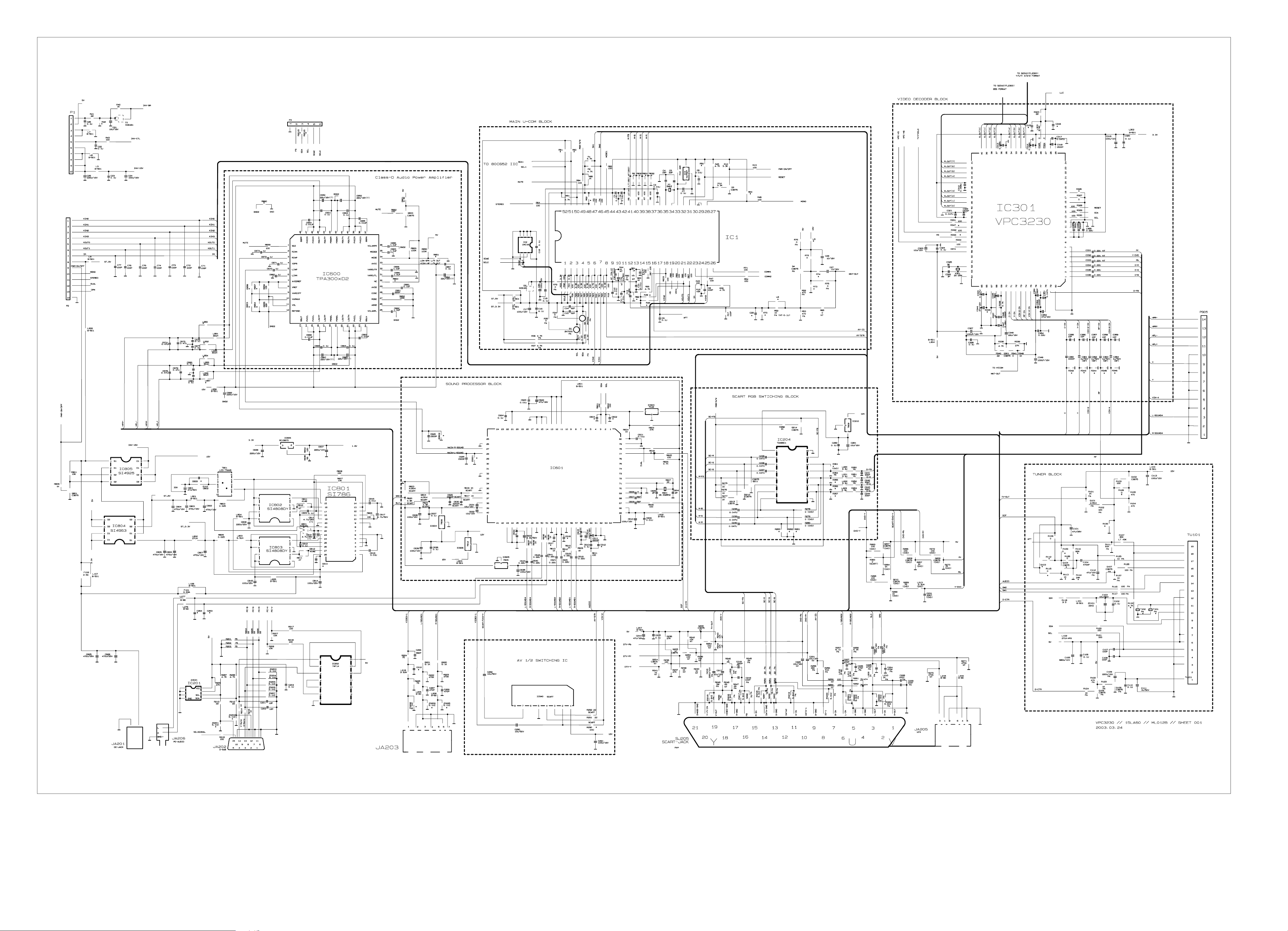
P/NO:3854VA0129A-S1(1/2)
2003.06.13
Page 29
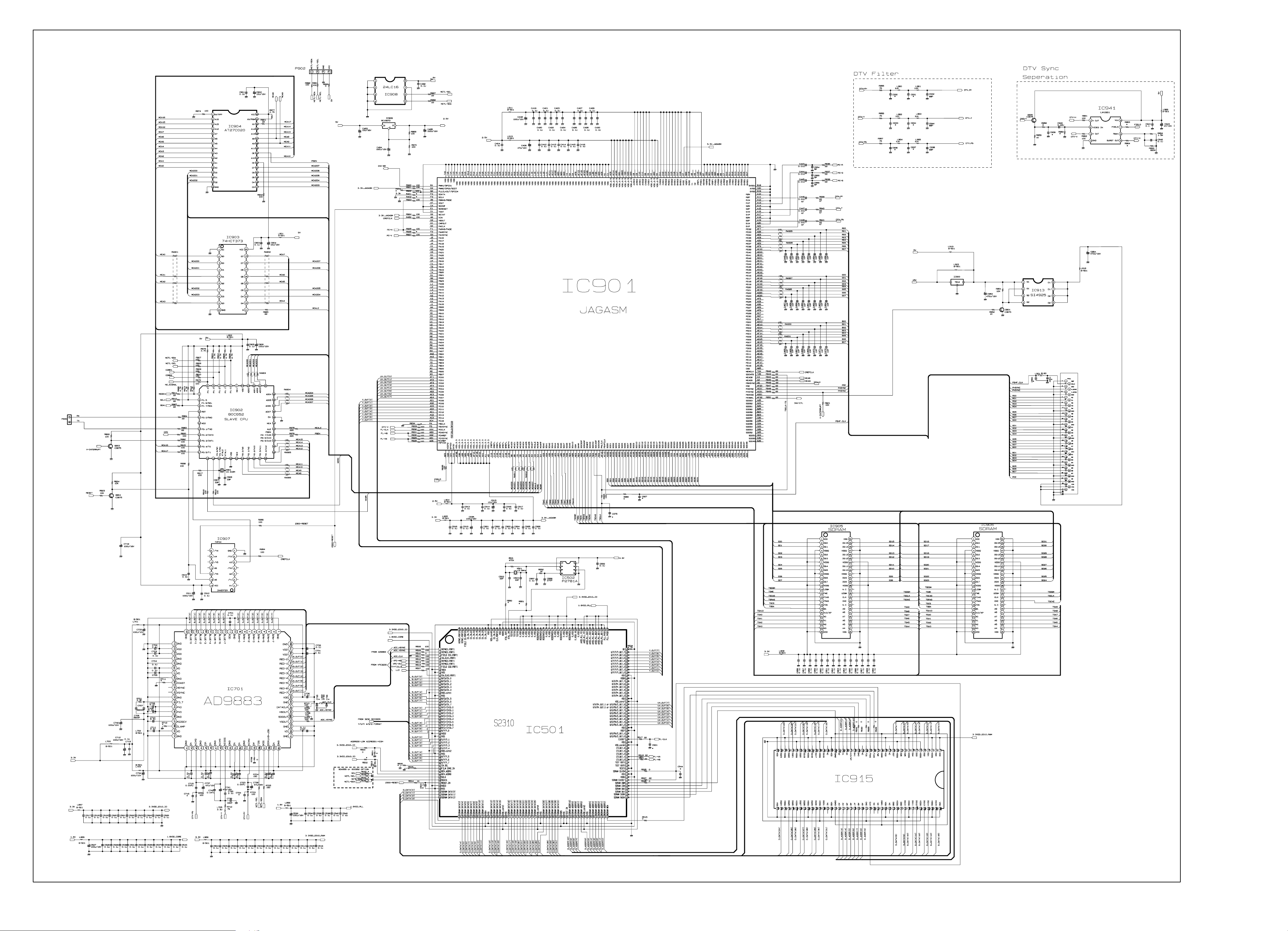
P/NO:3854VA0129A-S1(2/2)
2003.06.13
Page 30

Sep.,2003
Printed in KoreaP/NO : 3828VD0154D
 Loading...