

Page 1

HDD/DVD RECORDER
SERVICE MANUAL
MODELS : RH199/RH199H
MODELS : RH199/RH199HSERVICE MANUAL
CAUTION
BEFORE SERVICING THE UNIT, READ THE “SAFETY PRECAUTIONS”
IN THIS MANUAL.
Page 2

CONTENTS
SECTION 1 . . . .SUMMARY
SECTION 2 . . . .CABINET & MAIN CHASSIS
SECTION 3 . . . .ELECTRICAL
SECTION 4 . . . .RS-01A LOADER PART
SECTION 5 . . . .REPLACEMENT PARTS LIST
Page 3

1-2
SECTION 1
SUMMARY
CONTENTS
NEW FUNCTIONS OF HDD/DVD-RECORDER................................................................. 1-2
PRODUCT SAFETY SERVICING GUIDELINES FOR VIDEO PRODUCTS.............. 1-3
SERVICING PRECAUTIONS .................................................................................................. 1-4
• General Servicing Precautions
• Insulation Checking Prodedure
• Electrostatically Sensitive Devices
SERVICE INFORMATION FOR EEPROM IC SETTING ................................................. 1-5
SPECIFICATIONS ...................................................................................................................... 1-6
Page 4

1-3
NEW FUNCTIONS OF HDD/DVD-RECORDER
• HDMI
HDMI IS THE SPECIFICATION FOR THE HIGH-DEFINITION MULTIMEDIA INTERFACE. HDMI IS PROVIDED FOR TRANSMITTING DIGITAL TELEVISION AUDIOVISUALSIGNALS FROM HDD-DVD RECORDER TO
TELEVISION SETS, OTHER VIDEO DISPLAYS. HDMI CAN CARRY HIGH QUALITY MULTI-CHANNEL
AUDIO DATAAND CAN CARRY ALL STANDARD AND HIGH DEFINITION CONSUMER ELECTRONICS
VIDEO FORMATS. CONTENT PROTECTION TECHNOLOGY IS AVAILABLE. HDMI CAN ALSO CARRY
CONTROL AND STATUS INFORMATION IN BOTH DIRECTIONS.
<< OPERATING >>
AUDIO, VIDEO AND AUXILIARY DATA IS TRANSMITTED ACROSS THE THREE TMDS DATA CHANNELS.
THE VIDEO PIXEL CLOCK IS TRANSMITTED ON THE TMDS CLOCK CHANNELAND IS USED BY THE
RECEIVER AS A FREQUENCY REFERENCE FOR DATA RECOVERY ON THE THREE TMDS DATA CHANNELS.
VIDEO DATAIS CARRIED AS ASERIES OF 24-BIT PIXELS ON THE THREE TMDS DATA CHANNELS.
TMDS ENCODING CONVERTS THE 8BIT PER CHANNEL INTO THE 10BIT DC–BALANCED.
VIDEO PIXEL RATES CAN RANGE FROM 25MHZ TO 165MHZ. THE VIDEO PIXELS CAN BE ENCODED IN
EITHER RGB,YCBCR 4:4:4 OR YCBCR 4:2:2 FORMATS. IN ALLTHREE CASES, UP TP 24 BITS PER
PIXEL CAN BE TRANSFERRED.
FAST DUBBING
DUBBING MEANS ACOPYING FUNCTION BETWEEN HDD TO DVD DISCS.
COPYING BETWEEN HDD TO DVD IS A COMPLETELY DIGITAL PROCESS AND THEREFORE INVOLVES
NO LOSS OF QUALITY IN THE AUDIO OR VIDEO. SO THIS MEANS THAT COPYING CAN BE CARRIED
OUT AT THE MAXIMUM SPEED POSSIBLE.
<< DUBBING SPEED RATE >>
NORMAL DUBBING : SPEED RATE MAX X1
FAST DUBBING : SPEED RATE MAX X4
WHEN FAST DUBBING FROM HDD TO DVD , THE SPEED OF COPYING DEPENDS ON THE RECORDING
MODE AND THE KIND OF USING THE DVD DISC, AND THIS MODE IS NOT AVAILABLE FOR EDITED
VIDEO TITLE IN HDD.
WHEN FAST DUBBING FROM DVD TO HDD , ONLY AVAILABLE WHEN COPYING VR MODE DISC(DVDRW) TO HDD , AND ONLY NORMAL DUBBING AVAILABLE WHEN COPYING VIDEO MODE DISC
(DVD+R/RW, DVD-R) TO HDD
Page 5
1-4
IMPORTANT SAFETY NOTICE
This manual was prepared for use only by properly trained audio-video service
technicians.
When servicing this product, under no circumstances should the original
design be modified or altered without permission from LG Electronics
Corporation. All components should be replaced only with types identical to
those in the original circuit and their physical location, wiring and lead dress
must conform to original layout upon completion of repairs.
Special components are also used to prevent x-radiation, shock and fire hazard. These components are indicated by the letter “x” included in their component designators and are required to maintain safe performance. No deviations
are allowed without prior approval by LG Electronics Corporation.
Circuit diagrams may occasionally differ from the actual circuit used. This way,
implementation of the latest safety and performance improvement changes
into the set is not delayed until the new service literature is printed.
CAUTION: Do not attempt to modify this product in any way. Never perform
customized installations without manufacturer’s approval. Unauthorized modifications will not only void the warranty, but may lead to property damage or
user injury.
Service work should be performed only after you are thoroughly familiar with
these safety checks and servicing guidelines.
GRAPHIC SYMBOLS
The exclamation point within an equilateral triangle is intended to
alert the service personnel to important safety information in the
service literature.
The lightning flash with arrowhead symbol within an equilateral triangle is intended to alert the service personnel to the presence of
noninsulated “dangerous voltage” that may be of sufficient magnitude to constitute a risk of electric shock.
The pictorial representation of a fuse and its rating within an equilateral triangle is intended to convey to the service personnel the
following fuse replacement caution notice:
CAUTION: FOR CONTINUED PROTECTION AGAINST RISK
OF FIRE, REPLACE ALL FUSES WITH THE SAME TYPE AND
RATING AS MARKED NEAR EACH FUSE.
SERVICE INFORMATION
While servicing, use an isolation transformer for protection from AC line shock.
After the original service problem has been corrected, make a check of the following:
FIRE AND SHOCK HAZARD
1. Be sure that all components are positioned to avoid a possibility of adjacent
component shorts. This is especially important on items trans-ported to and
from the repair shop.
2. Verify that all protective devices such as insulators, barriers, covers, shields,
strain reliefs, power supply cords, and other hardware have been reinstalled
per the original design. Be sure that the safety purpose of the polarized line
plug has not been defeated.
3. Soldering must be inspected to discover possible cold solder joints, solder
splashes, or sharp solder points. Be certain to remove all loose foreign particles.
4. Check for physical evidence of damage or deterioration to parts and components, for frayed leads or damaged insulation (including the AC cord), and
replace if necessary.
5. No lead or component should touch a high current device or a resistor rated
at 1 watt or more. Lead tension around protruding metal surfaces must be
avoided.
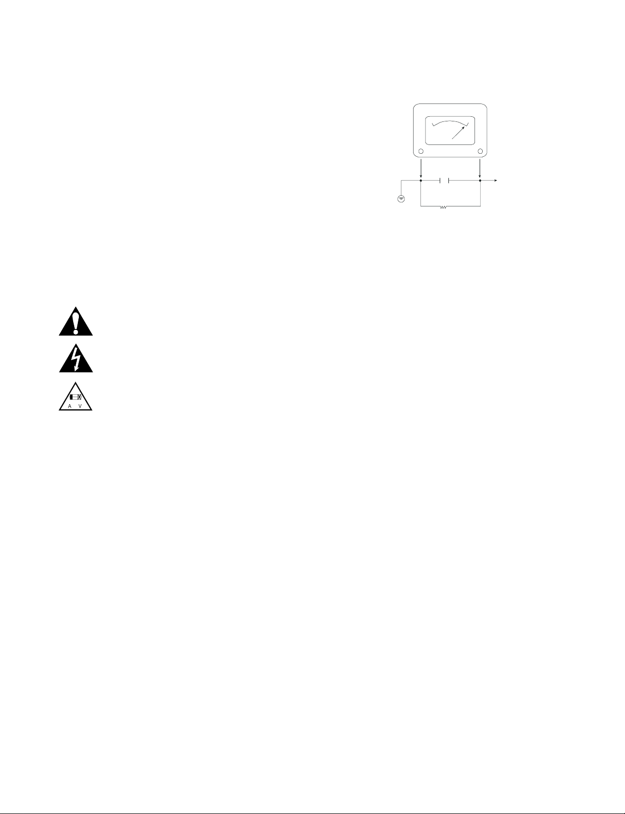
6. After reassembly of the set, always perform an AC leakage test on all
exposed metallic parts of the cabinet (the channel selector knobs, antenna
terminals, handle and screws) to be sure that set is safe to operate without
danger of electrical shock. DO NOT USE A LINE ISOLATION TRANSFORMER DURING THIS TEST. Use an AC voltmeter having 5000 ohms per
volt or more sensitivity in the following manner: Connect a 1500 ohm, 10
watt resistor, paralleled by a .15 mfd 150V AC type capacitor between a
known good earth ground water pipe, conduit, etc.) and the exposed metallic parts, one at a time. Measure the AC voltage across the combination of
1500 ohm resistor and .15 mfd capacitor. Reverse the AC plug by using a
non-polarized adaptor and repeat AC voltage measurements for each
exposed metallic part. Voltage measured must not exceed 0.75 volts RMS.
This corresponds to 0.5 milliamp AC. Any value exceeding this limit constitutes a potential shock hazard and must be corrected immediately.
TIPS ON PROPER INSTALLATION
1. Never install any receiver in a closed-in recess, cubbyhole, or closely fitting
shelf space over, or close to, a heat duct, or in the path of heated air flow.
2. Avoid conditions of high humidity such as: outdoor patio installations where
dew is a factor, near steam radiators where steam leakage is a factor, etc.
3. Avoid placement where draperies may obstruct venting. The customer
should also avoid the use of decorative scarves or other coverings that
might obstruct ventilation.
4. Wall- and shelf-mounted installations using a commercial mounting kit must
follow the factory-approved mounting instructions. A product mounted to a
shelf or platform must retain its original feet (or the equivalent thickness in
spacers) to provide adequate air flow across the bottom. Bolts or screws
used for fasteners must not touch any parts or wiring. Perform leakage tests
on customized installations.
5. Caution customers against mounting a product on a sloping shelf or in a tilted position, unless the receiver is properly secured.
6. A product on a roll-about cart should be stable in its mounting to the cart.
Caution the customer on the hazards of trying to roll a cart with small casters across thresholds or deep pile carpets.
7. Caution customers against using extension cords. Explain that a forest of
extensions, sprouting from a single outlet, can lead to disastrous consequences to home and family.
PRODUCT SAFETY SERVICING GUIDELINES FOR VIDEO PRODUCTS
A.C. Voltmeter
Good Earth Ground
such as the Water
Pipe, Conduit, etc.
0.15uF
1500 OHM
10 WATT
Place this probe
on each exposed
metal part.
Page 6

1-5
SERVICING PRECAUTIONS
CAUTION : Before servicing the HDD/DVD Recorder covered by this service data and its supplements and addends,
read and follow the
SAFETY PRECAUTIONS. NOTE : if
unforeseen circumstances create conflict between the following servicing precautions and any of the safety precautions in this publications, always follow the safety precautions.
Remembers Safety First:
General Servicing Precautions
1. Always unplug the HDD/DVD Recorder AC power cord
from the AC power source before:
(1)Removing or reinstalling any component, circuit board,
module, or any other assembly.
(2) Disconnection or reconnecting any internal electrical
plug or other electrical connection.
(3) Connecting a test substitute in parallel with an elec-
trolytic capacitor.
Caution : A wrong part substitution or incorrect
polarity installation of electrolytic capacitors may result
in an explosion hazard.
2. Do not spray chemicals on or near this HDD/DVD
Recorder or any of its assemblies.
3. Unless specified otherwise in this service data, clean
electrical contacts by applying an appropriate contact
cleaning solution to the contacts with a pipe cleaner,
cotton-tipped swab, or comparable soft applicator.
Unless specified otherwise in this service data, lubrication
of contacts is not required.
4. Do not defeat any plug/socket B+ voltage interlocks with
whitch instruments covered by this service manual might
be equipped.
5. Do not apply AC power to this HDD/DVD Recorder and/or
any of its electrical assemblies unless all solid-state
device heat sinks are cerrectly installed.
6. Always connect test instrument ground lead to the
appropriate ground before connection the test instrument
positive lead. Always remove the test instrument ground
lead last.
Insulation Checking Procedure
Disconnect the attachment plug from the AC outlet and turn
the power on. Connect an insulation resistance meter(500V)
to the blades of the attachment plug. The insulation resistance between each blade of the attachment plug and accessible conductive parts (Note 1) should be more than 1Mohm.
Note 1 : Accessible Conductive Parts including Metal panels, Input terminals, Earphone jacks, etc.
Electrostatically Sensitive (ES) Devices
Some semiconductor (solid state) devices can be damaged
easily by static electricity. Such components commonly are
called Electrostatically Sensitive (ES) Devices. Examples of
typical ES devices are integrated circuits and some field
effect transistors and semiconductor chip components.
The following techniques should be used to help reduce the
incidence of component damage caused by static electricity.
1. Immediately before handling any semiconductor component or semiconductor-equipped assembly, drain off any
electrostatic charge on your body by touching a known
earth ground. Alternatively, obtain and wear a commercially available discharging wrist strap device, which
should be removed for potential shock reasons prior to
applying power to the unit under test.
2. After removing an electrical assembly equipped with ES
devices, place the assembly on a conductive surface such
as aluminum foil, to prevent electrostatic charge buildup or
exposure of the assembly.
3. Use only a grouned-tip soldering iron to solder or unsolder
ES devices.
4. Use only an anti-static solder removal device. Some
solder removal devices not classified a “anti-static” can
generate electrical charges sufficient to damage ES
devices.
5. Do not use freon-propelled chemicals. These can
generate electrical charge sufficient to damage ES
devices.
6. Do not remove a replacement ES device from its protec
tive package until immediately before you are ready to
install it. (Most replacement ES devices are packaged with
leads electrically shorted together by conductive foam,
aluminum foil, or comparable conductive material).
7. Immediately before removing the protective material from
the leads of a replacement ES device, touch the protective
material to the chassis or circuit assembly into which the
device will be installed.
Caution : Be sure no power is applied to the chassis or
circuit, and observe all other safety precautions.
8. Minimize bodily motions when handling unpackaged
replacement ES devices. (Normally harmless motion such
as the brushing together of your clothes fabric or the lifting
of your foot from a carpeted floor can generate static electricity sufficient to damage an ES device.)
Page 7
1-6
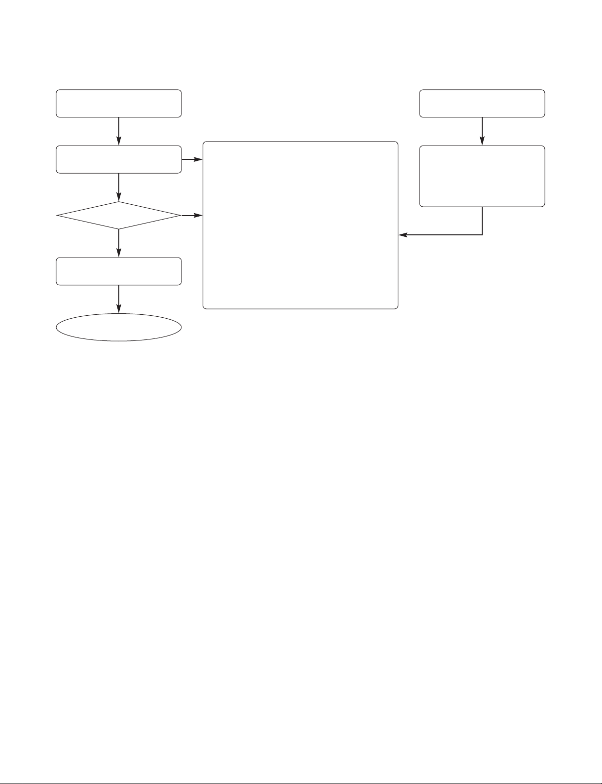
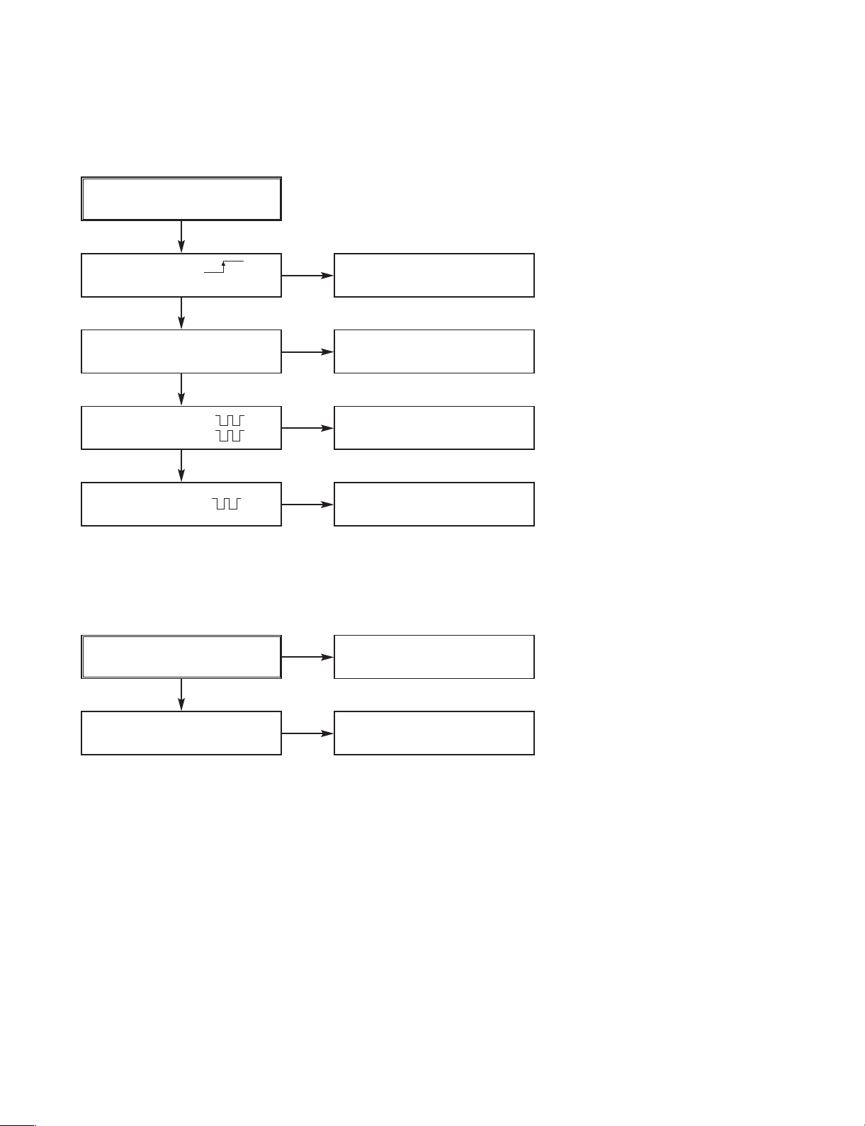
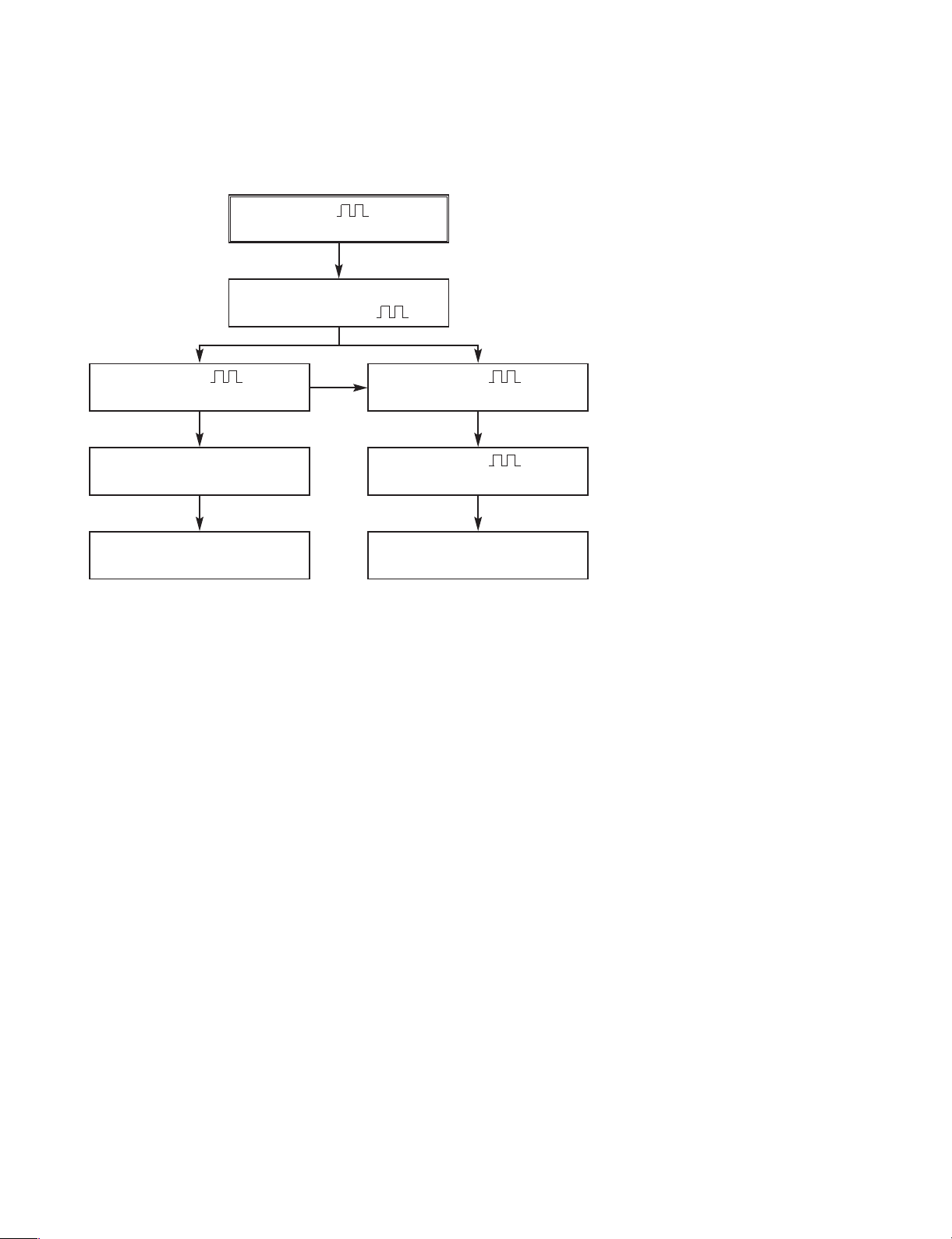
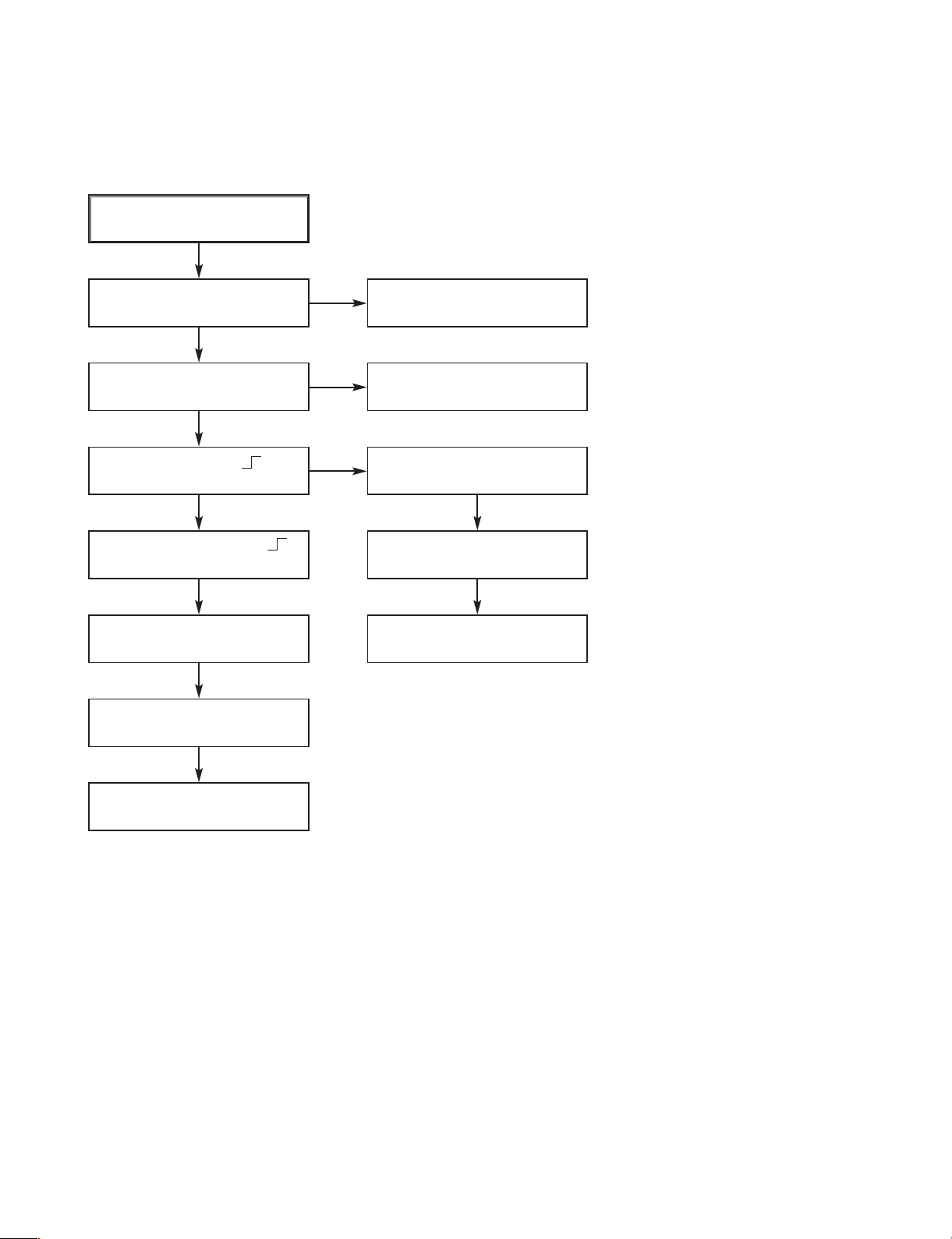
SERVICE INFORMATION FOR EEPROM IC SETTING
MICOM START
EEPROM ID CHECK
2 BYTE(B3,248,249)
MODEL NAME HEX BINARY
RH.S OPT1 00 00000000
OPT2 00 00000000
OPT3 00 00000000
OPT4 00 00000000 (reserved)
OPT5 00 00000000 (reserved)
OPT6 00 00000000 (reserved)
OPT7 00 00000000 (reserved)
OPT8 00 00000000 (reserved)
WRITE:OK EXIT:MENU,MP
MOVE:< > EDIT : __
OPTION WRITE : OK (OK KEY IN)
MASK : R00 , EEP : R00 , (D10)
(Each mask ,eeprom, It shows a development
release version.)
DETECT NEW EEPROM (OPTION EDIT SCREEN)
*** EEPROM INITIAL ***
- SETUP is displayed in the field if pressing the Front ch- & ch+ Key with the Remocon number "clear"
key pressed in the status of powering on.
- AUTO SEARCH is done since the initial screen of ACMS is serviced if powering on.
OPTION DATA READ
5TIME & COMPARE
MICOM NORMAL
OPERATION START
Press the "CLEAR" key on the
Remote controller and the "CH - "
key one the Front Panel the same
time, then it goes in to Tracking
initial mode.
OPTION CONFIRMATION MODE
ID OK?
No
No
Yes
Yes
Yes
Page 8

1-7
SPECIFICATIONS
• GENERAL
Power requirements AC 200-240V, 50/60 Hz
Power consumption 35W
Dimensions (approx.) 430 X 54 X 275 mm (w x h x d) without foot
Mass (approx.) 4.1 kg
Operating temperature 5°C to 35°C
Operating humidity 5 % to 90 %
Television system PAL I, B/G, I/I, SECAM D/K, K1 color system
Recording format PAL
• RECORDING
Recording format DVD Video Recording, DVD-VIDEO
Recordable media HDD (80GB), DVD-ReWritable, DVD-Recordable, DVD+ReWritable,
DVD+Recordable, DVD+Recordable (Double Layer)
Recordable time DVD (4.7GB): Approx. 1 hour (XP mode), 2 hours (SP mode),
4 hours (LP mode), 6 hours (EP mode)
DVD+R DL (8.5GB): Approx. 3 hour (XP mode),
3 hours 40 minutes (SP mode),
7 hours 10 minutes (LP mode),
10 hours 30 minutes (EP mode)
HDD (80GB): Approx. 20 hours (XP mode), 40 hours (SP mode),
74 hours (LP mode), 111 hours (EP mode)
Video recording format
Sampling frequency 27MHz
Compression format MPEG 2 (VBR support)
Audio recording format
Sampling frequency 48kHz
Compression format Dolby Digital
• PLAYBACK
Frequency response DVD (PCM 48 kHz): 8 Hz to 22 kHz, CD: 8 Hz to 20 kHz
DVD (PCM 96 kHz): 8 Hz to 44 kHz
Signal-to-noise ratio More than 100 dB (AUDIO OUT connector)
Harmonic distortion Less than 0.008% (AUDIO OUT connector)
Dynamic range More than 95 dB (AUDIO OUT connector)
• INPUTS
AERIAL IN Aerial input, 75 ohms
VIDEO IN 1.0 Vp-p 75 ohms, sync negative, RCA jack x 2 / SCART x 2
AUDIO IN 2.0 Vrms more than 47 kohms, RCA jack (L, R) x 2 / SCART x 2
S-VIDEO IN (Y) 1.0 V (p-p), 75 Ω, sync negative, Mini DIN 4-pin x 1
(C) 0.3 V (p-p) 75 Ω
DV IN 4 pin (IEEE 1394 standard)
• OUTPUTS
VIDEO OUT 1 Vp-p 75 Ω, sync negative, RCA jack x 1 / SCART x 2
S-VIDEO OUT (Y) 1.0 V (p-p), 75 Ω, sync negative, Mini DIN 4-pin x 1
(C) 0.3 V (p-p) 75 Ω
COMPONENT VIDEO OUT (Y) 1.0 V (p-p), 75 Ω, sync negative, RCA jack x 1
(Pb)/(Pr) 0.7 V (p-p), 75 Ω, RCA jack x 2
Audio output (digital audio) 0.5 V (p-p), 75 Ω, RCA jack x 1
Audio output (optical audio) 3 V (p-p), 75 Ω, Optical connector x 1
Audio output (analog audio) 2.0 Vrms (1 KHz, 0 dB), 600 Ω, RCA jack (L, R) x 1 / SCART x 2
Page 9

2-1
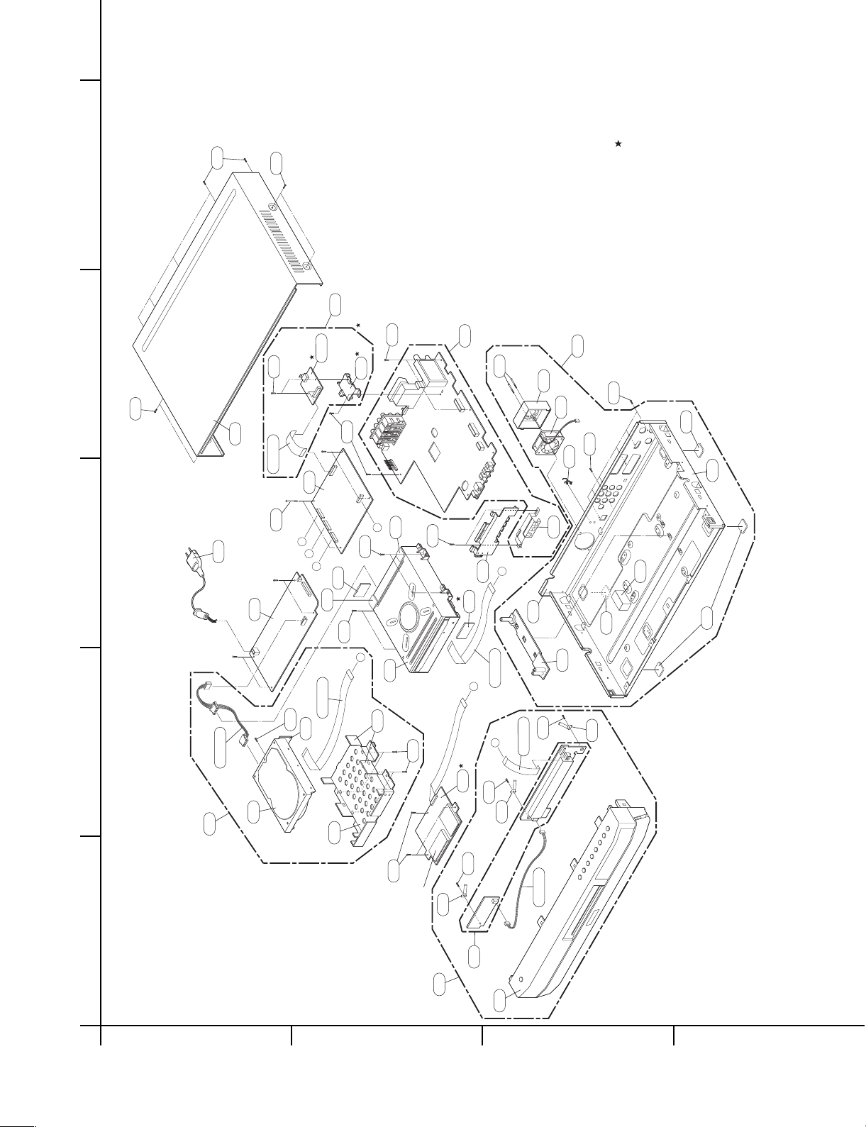
SECTION 2
CABINET & MAIN CHASSIS
CONTENTS
EXPLODED VIEWS ....................................................................................................................2-2
1. CABINET AND MAIN FRAME SECTION ................................................................................2-2
2. DECK MECHANISM SECTION(RS-01A) ................................................................................2-3
3. PACKING ACCESSORY SECTION .........................................................................................2-4
Page 10
2-2
EXPLODED VIEWS
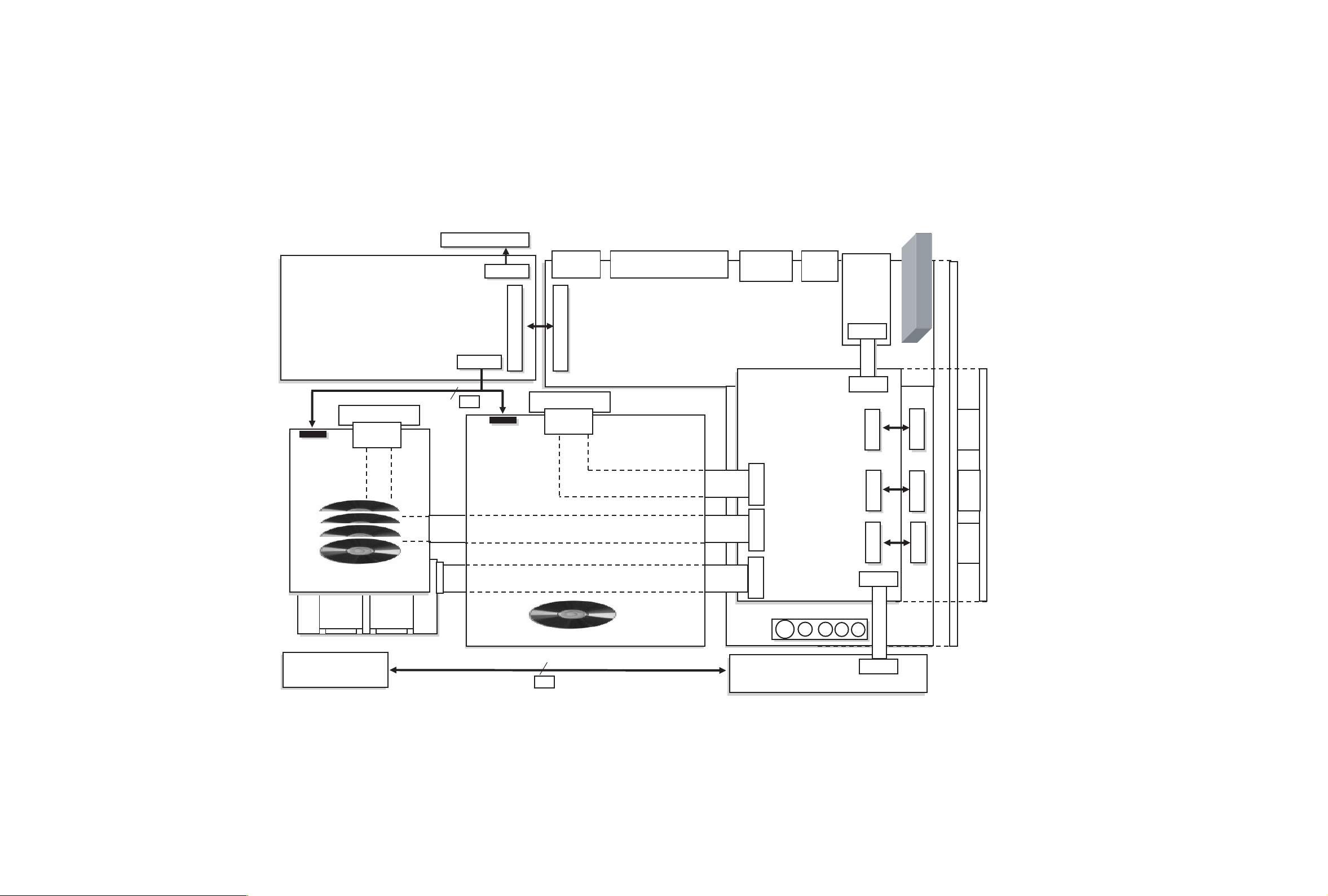
1. CABINET AND MAIN FRAME SECTION
A
5
4
3
2
1
BCD
463
463
250
463
468
CABLE3
A46
A54A
A54
HDMI
OPTIONAL PART
HDMI MODEL ONLY
BOARD
253
468
468
A52
I/O BOARD
OPTIONAL PART
A44
467
268
465
267
261
465
265
260
MAIN
C
A53
B
A
BOARD
A55
251
463
CABLE11
101
D
251
468
468
410
MEMORY
OPTIONAL
275
273
PART
272
A
OPTIONAL
PART
A56
452
452
C
CABLE5
D
275
463
B
A60
103
320
452
CABLE2
CABLE1
274
264
275
261
262
261
471
300
A47
SMPS
468
CABLE10
A26
104
A50
A43
280
Page 11
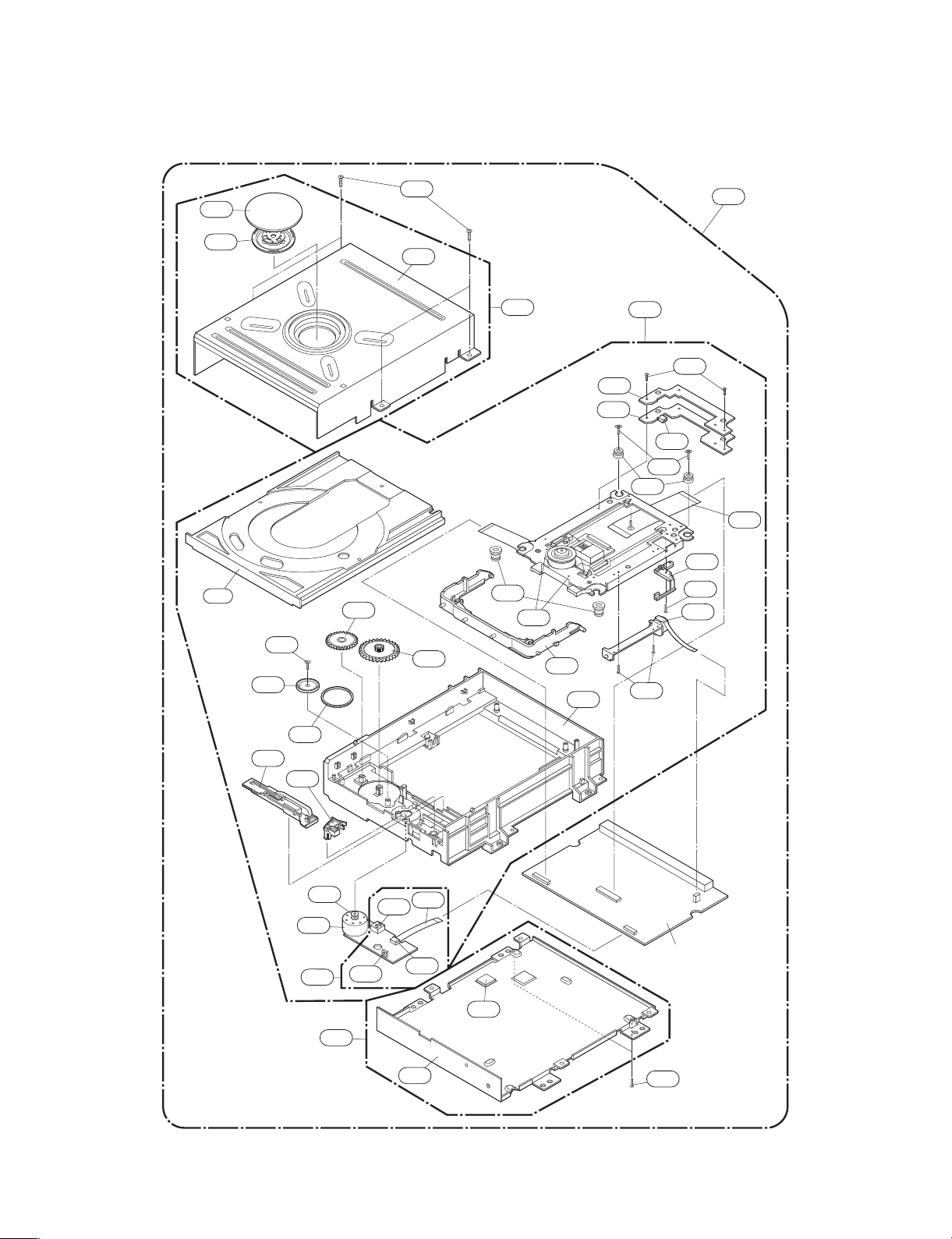
2-3
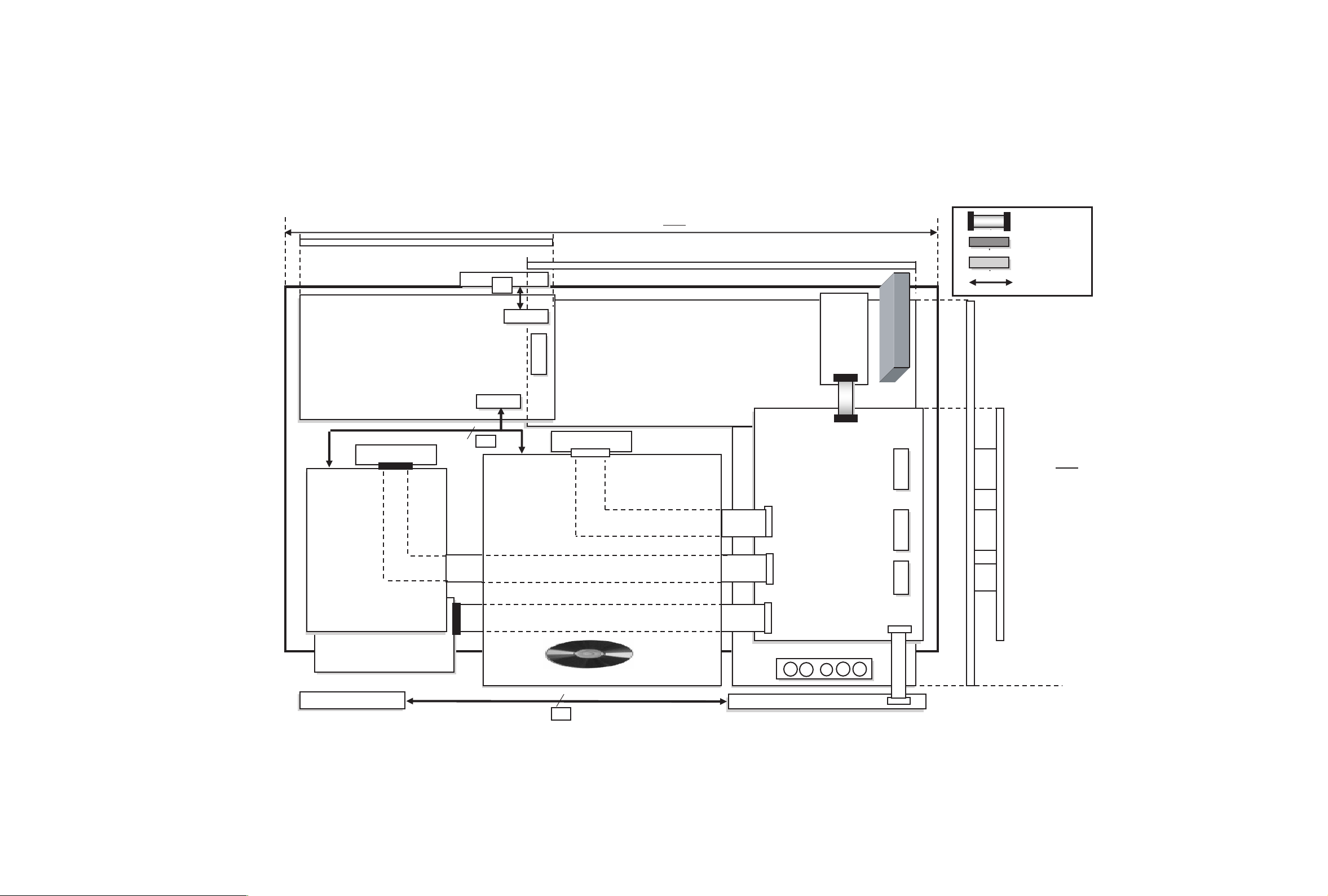
2. DECK MECHANISM SECTION(RS-01A)
1001
1003
1026
1017
1431
1002
A001
1041
1432
A60
A002
1434
1033
1032
1034
1437
1025
1030
1038
1432
1036
1433
1016
1012
1015
1014
1018
A005
1019
1048
1042
1043
1044
1047
1013
1045
1046
1011
1020
1432
Main C.B.A
1439
Page 12
2-4
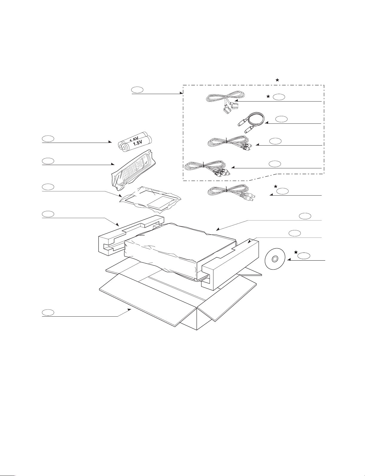
3. PACKING ACCESSORY SECTION
832
DISC
810
CABLE ASS'Y
OPTIONAL PART
821
SCART CABLE
Cable, Coaxial
806
808 Battery
Remote Control
900
Instruction Ass'y
801
Packing
803
Box
802
811
812
822
Plug Ass'y, 1Way
Plug Ass'y, 2Way
FLAT CABLE
Bag
804
803
Packing
Page 13

3-1
SECTION 3
ELECTRICAL
CONTENTS
HDR PART
ELECTRICAL TROUBLESHOOTING GUIDE......................................................................................................................3-2
1. POWER SUPPLY ON SMPS BOARD...........................................................................................................................3-2
2. POWER SUPPLY ON I/O BOARD ................................................................................................................................3-4
3. SYSTEM CIRCUIT PART ..............................................................................................................................................3-7
4. DISC NOT RECOGNIZED.............................................................................................................................................3-7
5. WHEN PLAYING DISC, NO AUDIO OUTPUT ..............................................................................................................3-8
6. NO OPTICAL / DIGITAL OUTPUT.................................................................................................................................3-9
7. NO TUNER AUDIO OUTPUT....................................................................................................... ...............................3-10
8. NO EXTERNAL INPUT AUDIO....................................................................................................................................3-11
9. NO RGB / COMPONENT VIDEO SIGNAL WHEN PLAY DISC..................................................................................3-12
10. NO COMPOSITE / S-VIDEO SIGNAL WHEN PLAY DISC.......................................................................................3-12
11. NO TV, EXTERNAL INPUT VIDEO SIGNAL ............................................................................................................3-13
12. NO DV(IEEE 1394) INPUT (VIDEO/AUDIO) SIGNAL...............................................................................................3-14
BLOCK DIAGRAMS............................................................................................................................................................3-16
1. OVERALL BLOCK DIAGRAM .....................................................................................................................................3-15
2. LAYOUT CONNECTION BLOCK DIAGRAM_1 ..........................................................................................................3-17
3. LAYOUT CONNECTION BLOCK DIAGRAM_2 ..........................................................................................................3-19
4. SMPS BLOCK DIAGRAM............................................................................................................................................3-21
5. POWER : MAIN BOARD BLOCK DIAGRAM..............................................................................................................3-23
6. POWER : I/O BOARD BLOCK DIAGRAM ..................................................................................................................3-25
7. IN/OUT BLOCK DIAGRAM ( SCART MODEL ONLY )................................................................................................3-27
8. VIDEO BLOCK DIAGRAM...........................................................................................................................................3-29
9. VIDEO S/W PATH BLOCK DIAGRAM................................................................................................ .........................3-31
10. AUDIO BLOCK DIAGRAM.........................................................................................................................................3-33
11. AUDIO S/W PATH BLOCK DIAGRAM.......................................................................................................................3-35
12. FLD / µ-COM / TUNER BLOCK DIAGRAM...............................................................................................................3-37
13. MAIN BLOCK DIAGRAM ( SCART MODEL ONLY ).................................................................................................3-39
14. TIMER BLOCK DIAGRAM.........................................................................................................................................3-41
CIRCUIT DIAGRAMS ..........................................................................................................................................................3-43
1. SMPS 1 CIRCUIT DIAGRAM......................................................................................................................................3-43
2. SMPS 2 CIRCUIT DIAGRAM......................................................................................................................................3-45
3. MPEG CIRCUIT DIAGRAM.........................................................................................................................................3-47
4. FLASH/DDR CIRCUIT DIAGRAM...............................................................................................................................3-49
5. RESET & 1394 & JEPG CIRCUIT DIAGRAM.............................................................................................................3-51
6. ATAPI & MEMORY CARD CIRCUIT DIAGRAM ..........................................................................................................3-53
7. I/O, µ-COM CIRCUIT DIAGRAM.................................................................................................................................3-55
8. TUNER/MPX/ADC/DAC/JACK CIRCUIT DIAGRAM...................................................................................................3-57
9. DECODER CIRCUIT DIAGRAM..................................................................................................................................3-59
10. TIMER CIRCUIT DIAGRAM ......................................................................................................................................3-61
•
WAVEFORMS ...................................................................................................................................................................3-63
• CIRCUIT VOLTAGE CHART ............................................................................................................................................3-65
PRINTED CIRCUIT DIAGRAMS.........................................................................................................................................3-71
1. MAIN P.C.BOARD .............................................................................................................. ..........................................3-71
2. I/O P.C.BOARD............................................................................................................................................................3-73
3. POWER P.C.BOARD...................................................................................................................................................3-77
4. TIMER1 P.C.BOARD ...................................................................................................................................................3-79
5. TIMER2 P.C.BOARD ...................................................................................................................................................3-81
6. HDMI P.C.BOARD .......................................................................................................................................................3-83
Page 14
3-2
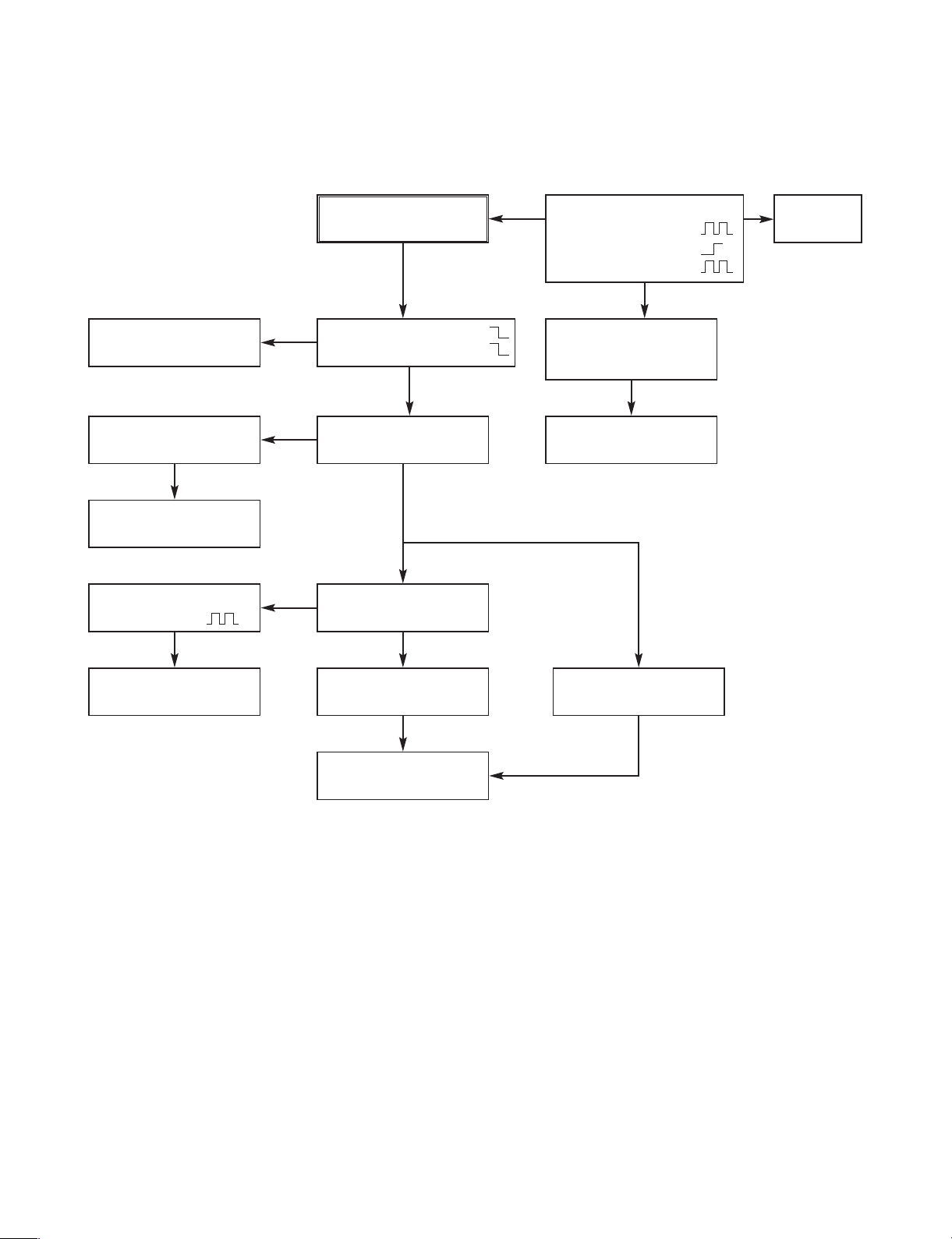
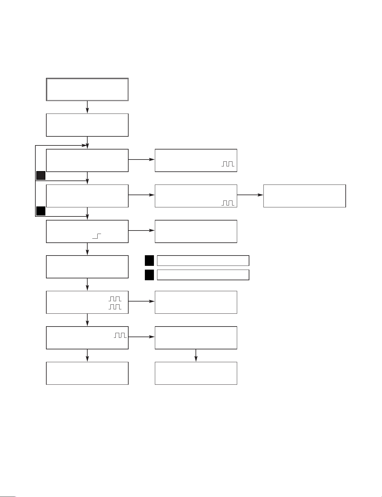
ELECTRICAL TROUBLESHOOTING GUIDE
HDR PART
Replace the BD101
Replace the F101
(Use the same Fuse)
No 5.3VA
Is the F101 Normal?
Is the TH01 Normal?
Is the Vcc (10V - 17V)
supplied to IC101 Pin6?
Is the BD101 Normal?
Is the D128 normal?
Is there about 2.5V at the
IC103 Pin1?
Is the D121 normal?
Is the D122 Normal?
Is the D125 Normal?
Is the D124 Normal?
Is the D127 Normal?
Is the D126 Normal?
NO
NO
NO
NO
NO
NO
NO
NO
NO
NO
NO
NO
YES
YES
YES
YES
YESYES
YES
YES
YES
YES
YES
YES
YES
YES
Replace the TH101
Is the D102 normal?
Check or Replace the
D102
Replace the D128
Replace the IC103
Replace the D121
Replace the D122
Replace the D125
Replace the D124
Replace the D127
Replace the D126
1. POWER SUPPLY ON SMPS BOARD
Power Line of I/O PCB
is short
Page 15
3-3
No 5V for HDD &
DVD Drive
Check D125 and
Replace
Is there about 5.5V
at the IC156 pin1?
Is there about 4V ~ 5V
at the IC156 pin 4?
NO
NO
Check the ‘PWR CTL
“H”’ signal from µ-COM
YES
YES
Check the IC156
and Replace
YES
No 12V for HDD &
DVD Drive
Check D124 and
Replace
Check the ‘PWR CTL
“H”’ signal from µ-COM
Is there about 13.5V
at the IC155 pin1?
Is there about 4V ~ 5V
at the IC155 pin 4?
Check the IC155
and Replace
NO
NO
YES
YES
YES
Page 16
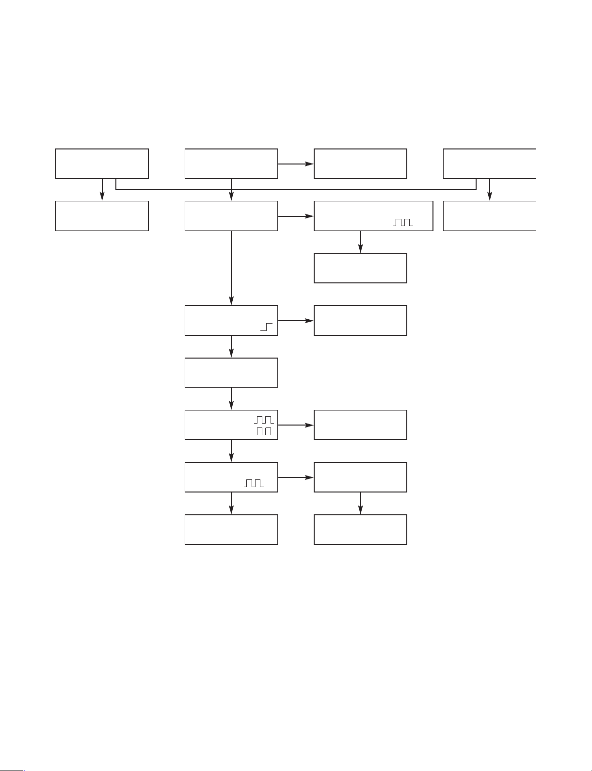
3-4
2. POWER SUPPLY ON I/O BOARD
No 33VT
Is the VCC (33V) supplied to Q161 Emitor?
Check D126 on SMPS
Board and Replace
Is there about 0V
at Q152 Collector?
Check Q161 and
Replace
Check the ‘TIMER H’
signal from µ-COM
Is there about 5V at R180
and 0.7V at Q152 Base?
Check Q152 and
Replace
YES
YES
YES
No 5VT
Check 5.3VA on
SMPS Board
Check Q155 and
Replace
Is the VCC (5.3V) supplied to Q155 Emitor?
Is there about 0V at D152
and Q152 Collector?
Is there about 5V at R180
and 0.7V at Q152 Base?
NO
NO
Check the ‘TIMER H’
signal from µ-COM
NO
YES
YES
YES
Check Q152 and
Replace
YES
No 12V
Check D124 on SMPS
Board and Replace
Check Q164 and
Replace
Check D126 on SMPS
Board and Replace
Check Q162 and
Replace
Check the ‘PWR CTL
H’ signal from µ-COM
Is the VCC (14V) supplied to Q164 Collector?
Is there about 12.5V at
ZD151 & Q164 Base?
Is the VCC (33V) supplied to Q162 Emitor?
NO
NO
NO
NO
NO
YES
YES
YES
Is there about 0V
at Q162 Base?
YES
Is there about 5V at R171
and 0.7V at Q156 Base?
YES
Check Q156 and
Replace
YES
No 5.2V
Check 5.3VA on
SMPS Board
Is the VCC (5.3V) supplied to Q151 Emitor?
Is there about 0V at D153
and Q156 Collector?
NO NO
Check Q151 and
Replace
Check the ‘PWR CTL
H’ signal from µ-COM
NO
NO
NO
NO
YES
YES
Is there about 5V at R171
and 0.7V at Q156 Base?
Check Q156 and
Replace
YES
YES
Page 17
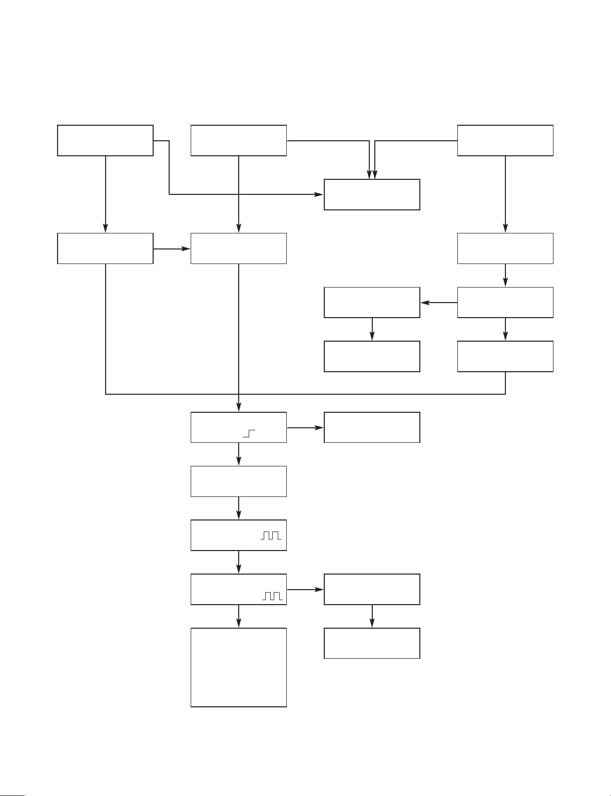
3-5
No SW_5.3VA
Is the VCC (5.3V) supplied to Q158 Emitor?
Check 5.3VA on
SMPS Board
Is there about 0V
at R179 and R156?
Check the ‘STANBY
H’signal from µ-COM
Check Q158 and
Replace
YES
YES
YES
No 3.3V
Check or Replace
the D127
Check the ‘PWR CTL
“H”’signal from µ-com
Is there about 3.8V at
the IC152 pin1?
Is there about 4V~ 5V
at the IC152 pin4?
Check the IC152
and Replace
NO
NO
YES
YES
YES
No 5.0VD
Check 5.3VA on
SMPS Board
Check the ‘PWR CTL
H’ signal from µ-COM
Is there about 5.3V
at the IC153 pin 1?
Is there about 4V ~ 5V
at the IC153 pin 4?
Check the IC153
and Replace
NO
NO
YES
YES
YES
No 2.5V
Check D154 and
D127 on SMPS Board
Is there about 3V ~ 3.8V
at the IC151 pin 1?
Is there about 4V ~ 5V
at the IC151 pin 4?
NO NO
Check the ‘PWR CTL
H’ signal from µ-COM
NO NO
YES
YES
Check the IC151
and Replace
YES
Page 18
3-6
No SW_FD(+)
Check D121 on SMPS
Board and Replace
Check Q163 and
Replace
Is the VCC (FD+) supplied to Q163 Collector ?
Is there about 5.3V at R184
and Q153 Collector ?
Is the VCC (5.3V) supplied to Q153 Emitor ?
NO
NO
Check 5.3VA on
SMPS Board
NO
Check the ‘STANBY
H’ signal from µ-COM
NO
YES
YES
YES
Is there about 0V
at Q153 Base ?
YES
Check Q153 and
Replace
YES
No SW_12VG
Check D124 on SMPS
Board and Replace
Check Q165 and
Replace
Is the VCC (14V) supplied to Q165 Collector?
Is there about 12.5V at
ZD152 & Q165 Base?
Is the VCC (33V) supplied to Q160 Emitor?
NO
NO
Check D126 on SMPS
Board and Replace
NO
Check Q160 and
Replace
NO
Check SW_5.3VA
NO
YES
YES
YES
Is there about 0V at
Q160 Base?
YES
Is there about 5.3V
at Q166 Base?
YES
Check Q166 and
Replace
YES
No 1.25V
Check D155 and
2.5V power supply
Check Q159 and
Replace
Is the VCC (2V) supplied
to Q154 Emitor ?
Is there about 2V ~ 2.5V at
Q154 Base and IC154 pin 4?
Is the VCC (3.3V) supplied IC154 pin 1,2,8 ?
NO
NO
Check 3.3V power
supply
NO
YES
YES
YES
Check IC154 and
Replace
YES
No 1.8V
Check 3.3V power
supply
Check Q159 and
Replace
Is the VCC (3.3V) supplied to Q159
Emitor And IC154 pin 1,2,8 ?
Is there about 3V ~ 3.3V at
Q159 Base and IC154 pin 3 ?
Check IC154 and
Replace
NO
NO
YES
YES
YES
Page 19
3-7
“Please wait” displayed
Continue at Power On
Check PVM02 pin 13
IC 701 pin 19 (R714)
IC1306 pin 5 : ?
(/HOST-RESET)
X1101 : Clock oscillated?
(13.5MHz)
NO
Replace X1101
NO
Check IC1201 (Flash
Memory) & IC1101
NO
IC1101 DEFECT
NO
YES
YES
R11A9 : ?
IC1201 pin 32 : ?
YES
R1173, R1174 : ?
YES
3. SYSTEM CIRCUIT PART
Check Driver Power?
5V,12V
Change MEDIA TEST
Check A TAPI Interface
PLL1604 & PML07
Check SMPS
NO
NO
YES
4. DISC NOT RECOGNIZED
Page 20
3-8
CHECK IC803 pin 2,4 (VCC):12V
Pin 32,33 (SCL/SDA) :
IC808 pin 14,19 (Z_mute_R/L) :
IC701 pin 58 (A_mute_L) :
CHECK
IC808 pin 1,2,3,4 :
Pin 10 (Reset “H”)
Pin 7,8 (I2C) :
5. WHEN PLAYING DISC, NO AUDIO OUTPUT
CHECK
IC808 pin 17 (12V)
pin 5,11,20 (3.3V)
Replace IC808
YES
YES
IC808 pin 15,18(Audio_out R/L):
Is there a signal?
IC801 pin 1,7
Is there a signal?
IC803 pin 21,22,25,26
: Is there a signal?
CHECK Q801, Q802, Q803,
Q805, Q806, Q807, Q808
CHECK IC801 pin 8
(12V)
Replace IC801
Replace IC803
IC101
DEFECT
NO
L822, L823 :
Is there a signal?
YES
YES
YES
YES
YES
YES
YES YES
Only “Without SCART model”
L806, L826, L825, L810
: Is there a signal?
CHECK Cable connections & TV Audio mute.
NO
NO
NO
NO
Page 21
3-9
R1107 :
Is there a signal ?
CHECK PVM01 pin 1
(SPDIF_OUT) :
C856 :
Is there a signal ?
BD817 :
Is there a signal ?
CHECK JK802 &
RCA cable connection
NO
YES
YES
YES
YES
YES
YES
R851 :
Is there a signal?
CHECK
JK803 pin 2 (5.2V)
CHECK JK803 &
Optic cable connection
6. NO OPTICAL / DIGITAL OUTPUT
Page 22
3-10
7. NO TUNER AUDIO OUTPUT
TU701 pin 16 (SIF) :
Is there a signal?
C928,C963 :
Is there a signal?
IC903,904 pin 7 :
Is there a signal?
Replace IC803
CHECK
IC903,904 pin 6 (12V)
YES
YES
IC803 pin 20, 24, 23, 27
Is there a signal?
YES
IC901 pin 34 Or R999
(reset “H”) :
YES
X901 (24.576MHz) clock
oscillated ?
R902,R913,R997 :
R962,R978 (I2C) :
YES
YES
C901 pin 173 & R903 :
Is there a signal ?
When playing DISC,
no Audio output
YES
YES YES
NO
CHECK
IC 803 pin 2,4 (VCC) : 12V
Pin 32,33 (SCL/SDA) :
NO
CHECK
IC1302 Reset Circuit
NO
NO
NO
IC1101 DEFECT
CHECK
IC901 power 3.3V & 1.8V
IC901 DEFECT
YES
A
B
A
B
Only “P Model”
Only “Without SCART Model”
Page 23
3-11
8. NO EXTERNAL INPUT AUDIO
CHECK IC 803 pin 2,4 (VCC):12V
Pin 32,33 (SCL/SDA):
CHECK Cable connections & Input signal.
Replace IC803
CHECK IC1302
Reset Circuit
NO
YES
YES
IC803 pin 20, 24, 23,
27 : Is there a signal?
CHECK Cable connections & Input signal.
C979, C980 :
Is there a signal?
IC803 pin 10,16 :
Is there a signal?
C976,C977 :
Is there a signal?
< AV3 > < AV1/AV2 > < AV4 >
NO
IC901 pin 34 Or
R999 (reset”H”) :
X901 (24.576MHz)
clock oscillated?
NO
IC1101 DEFECT
NO
CHECK IC901
power 3.3V & 1.8V
NO
IC901 DEFECT
NO
YES
YES
YES
YES
R902,R913,R997 :
R962,R978 (I2C) :
YES
C901 pin 173
or R903 :
YES
When playing DISC,
no Audio output
YES
CHECK Cable connections & Input signal.
NO
Page 24

3-12
9. NO RGB / COMPONENT VIDEO SIGNAL WHEN PLAY DISC
R1153,R1154,R1155 :
Is there a signal ?
PVM01 pin 2,6,10 :
Is there a signal ?
IC802 pin 18,21,24 :
Is there a signal?
CHECK SW801 status &
SW801 pin 2 (RGB_SEL”H”)
NO
CHECK IC802 pin
1,16 (5.2V)
Replace IC802
YES
YES
YES
YES
10. NO COMPOSITE / S-VIDEO SIGNAL WHEN PLAY DISC
R1150,1151,1152 :
Is there a signal ?
PVM01 pin 14, 18, 22
: Is there a signal?
IC802 pin 27,30,32:
Is there a signal ?
CHECK RCA & S-Video
cable connection
IC803 pin 29,30 :
Is there a signal ?
NO
CHECK IC802 pin
1, 16 (5.2V)
NO
Replace IC802
YES
CHECK IC803 pin 2,4 (VCC) : 12V
Pin 32,33 (SCL/SDA) :
YES
YES
YES
CHECK SCART
cable connection
YES
Replace IC803
YES
A B
A
B
S-Video & RCA
SCART
Page 25
3-13
11. NO TV, EXTERNAL INPUT VIDEO SIGNAL
CHECK Cable connection & Input signal
C859, C869, C871:
Is there a signal?
IC 803 pin 21, 22, 25,
26 : Is there a signal?
C926 : Is there a
signal?
CHECK IC 803 pin 2,4 (12V)
Pin 32,33 (SCL/SDA)
Replace IC803
CHECK IC1302
Reset Circuit
CHECK IC901 power
3.3V & 1.8V
IC901 DEFECT
C917,C923,C934 :
Is there a signal ?
C618 : Is there a
signal ?
No video signal of external
input AV3 (Rear RCA input)
No video signal of external
input A V4(Composite/S-Video)
When Cable connecting Tuner and Rear
SCART1,2 No TV video signal (AV1/2)
NO
NO
NO
NO NO
NO
NO
YES
YES
YES
YES
YES
YES
YESYES
YES
IC901 pin 34 Or R999
(reset”H”) :
X901 (24.576MHz)
clock oscillated ?
YES
R962,R978 (I2C) :
IC901 pin 108 or
R930 (VI_CLK) :
CHECK No RGB /
Component /
Composite /
S-Video
Signal when play
DISC
YES
YES
YES YES
Page 26
3-14
12. NO DV(IEEE 1394) INPUT (VIDEO/AUDIO) SIGNAL
Check DV_Jack connection
DV-mode switching ?
IC1401 power 3.3V
IC1401 pin 37 : “High”
& X401 (24.576MHz) oscillated ?
NO
IC1401 power 3.3V
NO
Change to DV-mode.
Using Remote Control
NO
CHECK IC1302 Reset Circuit
YES
YES
YES
IC1401 pin 15 : “High”
Is there a signal?
YES
IC1401 pin 1,27,28,29,30 :
Is there a signal?
YES
IC1401 pin 2, 3 :
Is there a signal?
YES
IC101 DEFECT
YES
CHECK DV Cable
YES
Replace IC1401
YES
Page 27

Page 28
3-15 3-16
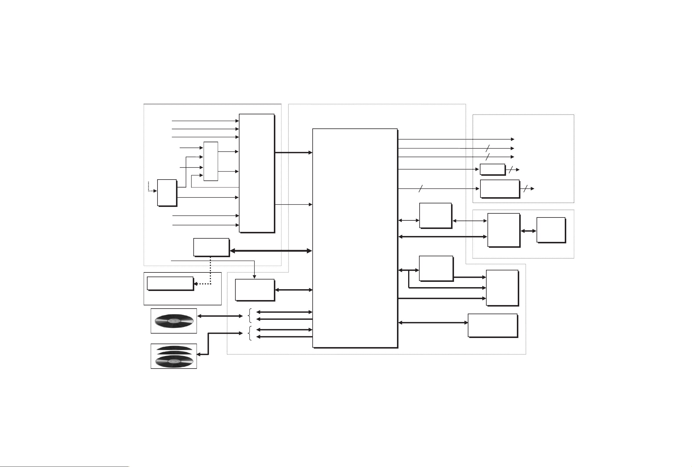
BLOCK DIAGRAMS
1. OVERALL BLOCK DIAGRAM
I/O Board
V3_In
V4_In
S_In
V.S1/V.S2
A.S1/A.S2
RF
Tuner
Tuner
A3_In
A4
_In
DV_In
Front Driv er IC
Front Driv er IC
Front Timer Boa r
SW
U-COM
U-COM
d
AV_DEC
AV_DEC
Decoder
Decoder
SAA7137
SAA7137
PHY
PHY
TSB41AB1
TSB41AB1
MAIN Board
SIO_SPI_CS0
SIO_SPI_CLK
SIO_SPI_MISO
SIO_SPI_MOS
VIN_D[9:
AIN_D0
I
SPI I/O Interface
BIO_PHY_DATA[0:7]
0]
DMN8653
VOUT_CVB
VOUT_Y/C
VOUT_Y/Pb/Pr_R/G/B
AOUT_IEC958
AOUT_DO
ATA_CONTROL
HD[0:15]
HD[0:15]
HA[1:5],[23:22]
I/O Board
S
S/PDIF
S/PDIF
A_DAC:2ch
A_DAC:2ch
CS4351
CS4351
Buffer
Buffer
74LVC541
74LVC541
PHY
PHY
SAIN
SAIN
ASTEL
ASTEL
CVBS_Out
S_VIDEO_Out
Y/Pb/Pr or R/
Optical & Digital
Audio Out
Analog
Audio Out
G/B
SOCKET
SOCKET
x2
x2
Memory Board
Latch
Latch
74LVT16373
74LVT16373
HA[6:21]
Flash
Flash
64M-Bit
64M-Bit
DVD DRIVE
HDD DRIVE
ATAPI1_DATA[0:15]
ATAPI1 _...
ATAPI2_DATA[0:15]
ATAPI2 _...
DDR SDRAM
DDR SDRAM
512M-Bit
512M-Bit
Page 29
3-17 3-18
2. LAYOUT CONNECTION BLOCK DIAGRAM_1
SMPS Board
SMPS Board
Junction B'd
Junction Bíd
ATAPI2
5V
12V
FAN
P1D01
P1D01
4pin
P104
P104
12V
P1701
P1701
Junction Bíd
Junction Bíd
5V
FD(+)
FD(-)
-28VA
14VA
33VA
3.8VA
PWVS1
PWVS1
5.3VA
PWR_CTL_H
ATAPI1
AV3/Comp /DigitalOptical
Scart1/
Scart2SVideo
INPUT / OUTPUT Board
INPUT / OUTPUT Board
HDMI
PHM01
30 pin
TUNER
PMH10
PMV01
40:250mm
PMV01
PVM01
PVM01
I/O Board
30
Main Board
HDD
HDD
HARD DISC DRIVE
7-in-2 Memory
Key Board
DVD ± RW DRIVE
2pin
40pin
40pin
40pin
MAIN Board
MAIN Board
PML07PML08
PMC09
Front J ack
S
DV
TIMER Board
30
PMV02
PMV02
PVM02
PVM02
12
PMV04
PMV04
PVM02
PVM02
PMT05
16 pin
V
A
A
PMT01
Page 30
3-19 3-20
3. LAYOUT CONNECTION BLOCK DIAGRAM_2
SMPS B'd
SMPS
SMPS
Junction B'd
Junction Bíd
HDD
HDD
4pin
FAN
4pin
4pin
2pin
2pin
12pin
12pin
Junction B'd
Junction Bíd
430
I/O B'd
I/O Board
I/O Board
40pin
40pin
HDMI
30 pin
40:250mm
Main Board
Main Board
X pin
X pin
: FFC
X pin
X pin
X pin
X pin
: B'd t
: B'd i
o B'd
n
: Harness
I/O B'd
30pin
30
30pin
275
Main B'd
30
30pin
30pin
12
12pin
12pin
7-in-2 Memory
7-in-2 Memory
KeY B'd
DVD ± RW DRIVER
2pin
40pin
DV
S
V
Timer(FLD)
16 pin
A
A
Page 31

3-21 3-22
4. SMPS Block Diagram
BD101
A
C
NOISE FILTER
BLOCK
V101,C101,C102,
R101,L101
FUSE
F101
RECTIFIER &
TH0
B
D
1
C103
SNUBER
BLOCK
D101,R104,
C105,C106
T101
DRIVE & S/W
BLOCK
IC101,D102,R105,
ZD101,ZD103,
R109,C104,C107,
C108,C109, BC101
SMOOTHING BLOCK
D121,FR121,C120,R181,
R191,R131,ZD121
RECTIFIER &
SMOOTHING BLOCK
D122,C122,R122
5V RECTIFIER &
SMOOTHING BLOCK
D125,C121
14V RECTIFIER &
SMOOTHING BLOCK
D124,C123,L123,C133
3.8V RECTIFIER &
SMOOTHING BLOCK
D127,C124,L124,C134
33V RECTIFIER &
SMOOTHING BLOCK
D126,C126,R147,ZD122
P1701
FD(+)
FD(-)
-28V
14VA
3.8VA
33VA
5.3VA
PWR CTL
BR BL
(BK)(WH)
Y CAP
C112
!
Y CAP
C113
5.3V RECTIFIER &
SMOOTHING BLOCK
D128,C125,L125,C135
PHOTO COUPLER
IC102
ERROR AMP
IC103
FEEDBACK
BLOCK
R141,R142,
R143,R144,
R145,R146,
C143
5V REG &
S/W BLOCK
IC156,R156,
C156
12V REG &
S/W BLOCK
IC155,R155,
C155
P1D01
5V
12V
P104
FAN
Page 32

3-23 3-24
5. Power : Main Board Block Diagram
3.3V
3V3A
1.25V
V33_JED
3.3VA
DAC 3.3
V33_E5_VPA
V33_E5_VDDRE
F
E5_AVDD1
E5_AVD
AVDD_SYSPLL
IC 801
TC90A73UG
E5_1
V
V25
D
D2
V33_FLASH V33_FL ASH
FLASH
FLASH
DMN8653
SDRAM
V33_STB
+5V_STB
5V
5VD
V25_SSTL2
V33_BREG
74LVT16373
74LVT16373
74HCT125
74HCT125
74LVT273
74LVT273
HDD IF
MEMORY CARD IF
2.5V
3V3D
5VD
LOADER IF
HDMI IF
74LVC08
74LVC08
74LVC04
74LVC04
74LVC541A
74LVC541A
V18_HDMI
0.8T(500mA)
0.8T(700mA)
0.8T(400mA)
V33_PHY_A
1.8V
V33_PHY_D
TSB41AB1
5V
3.3V
2.5
V
V33_JEA
VREF
78
56
34
1 2
VTT
LP2955
(180mA)
2.0T(1.6A)
I/O U-COM PWR CTL
1.25V, 1.8V, 2.5V, 3.3V, 5VPWR_CTL_H
1.8V
1.25V
Page 33

3-25 3-26
6. Power : I/O Board Block Diagram
5
.3VA
U-COM
(MN101DF10GAF)
Reset IC
(KIA7031P)
PWR Fail
(KIA7042)
EEPROM
(24LC16B)
VPS/PDC
(SDA5650)
Tuner
Etc Logi c
SYS_5.3VA
5VT
(MN101DF10GAF)
U-COM
V 6dB Amp
(MM1
510)
5.2V
Video S/W
(BH
7868FS)
Optical Drive
12V
A.SW
(NJM
2521)
Diff OP AMP
(NJM
4580)
DAC
(CS4351)
12VG(SW)
A/V.SW (C+)
(MM1443)
3.3V
A/V Decoder
(SAA7137)
I/O U-COM PWR CTL
33VT
Tuner
1.8V
5.2V, 12V, 3.3V, 1.8VPWR_CTL_H
5VT, 33VTTIMER_H
12VG(SW)STANBY_H
Page 34

3-27 3-28
7. IN/OUT BLOCK DIAGRAM ( SCART MODEL ONLY )
S/W
BLOCK
A
A
.3V
4V
5
1
SMPS
BLOCK
)
D(+
F
SW_FD(+)
SW_5.3VA
SW_12VG
FD(+)
FD(-)
-29VA
12V
5.3VA
5.2V
33VT
5VT
1.8V
3.3V
2.5V
5.0VD
V
1.25
H
_H
M
L_
I/O
_V
CA
C
SE
SE
I2
U_
U_
T
T
TUNER
TUNER
PAL
PAL
FRONT.AV IN
S-VIDEO IN
REAR.AV IN
DV IN
TPA+
TPATPB+
TPB-
IC1401
TSB41AB1
FT
A
MM1510
MM1510
6dB Buffer
6dB Buffer
TU_V_OUT
SECAM_AM
SIF
F_A_L/R_IN
F_CVBS_IN
F_Y_IN
F_C_IN
R_CVBS_IN
R_A_L/R_
BIO_LREQ
BIO_PHY_CTL0
BIO_PHY_CTL1
BIO_LI
BIO_PHY_CLK
BIO_LPS
BIO_PHY_D[7:0]
IC703
IC703
IN
NK_ON
/RST_PHY
1394_PD
POWER_CTL_H
TIMER_H
STANBY_H
MM1510
6dB Buffer
C
N
O
Y
D
S
_
F
_
N
I
N
I
A
A
CV.IN2
Option
IC708
IC708
MM1510
6dB Buffer
A_SEL
IC_OUT_L/R
IC901
SAA7137D
AV DECODE
]
K
0
:
L
C
S
_
N
I
A
T
K
9
[
N
I
D
_
CL
_
N
I
N
I
_M
V
V
IN
A
DMN8653
ENC/DEC
IC701
MN101DF10GAF
MICOM
I/O
C
AV
I2
D
IC707
IC707
SDA5650
SDA5650
VPS
VPS
IC904
NJM2521
IC903
NJM2521
Option
R
CS4351
N
K
I
L
A
C
M
_
_
S
T
/
R
N
C
I
2
I
V
7
3
1
A
7
A
S
IC1101
MAIN BOARD
IC808
DAC
K
L
C
O
M
_
_D
T
T
U
O
OU
A
A
C
N
Y
S
F
_
T
U
O
A
DAC_A
L/R_OUT
K
L
C
S
_
T
U
O
A
I2C I/O
A_MUTE_L
Z_MUTE_L/R
IC801
NJM4580
SW_A_OUT_L/R
SW_V_OUT
R_OUT
G_OUT
B_OUT
CVBS_OUT
Y_OUT
C_OUT
SPDIF_OUT
IC705
IC705
24LC16B
24LC16B
EEPROM
EEPROM
AUDIO Mute
AUDIO Mute
TU_V_OUT
TU_L/R_OUT
AV SWITCH
CVBSout
BH7868FS
BH7868FS
VIDEO
VIDEO
Buffer
I/O BOARD
RGB_SEL
I2C I/O
Block
Block
A_OUT_L/R
IC803
MM1443
Built in 6dB
IC802
IC802
Buffer
R(Pr)_OUT
G(Py)_OUT
B(Pb)_OUT
C_SEPA_OUT
Y_SEPA_OUT
SW801
A_OUT_L/R
RCA_V_OUT
R_SCART_IN
G_SCART_IN
B_SCART_IN
EU2_V_IN
EU2_A_IN_L/R
EU2_V_OUT
EU2_A_OUT_L/R
EU1_A_IN_L/R
EU1_V_IN
EU1_A_OUT_L/R
EU1_V_OUT
R_SCART_OUT
G_SCART_OUT
B_SCART_OUT
Pr_RCA_O UT
Y_RCA_OUT
Pb_RCA_OUT
S-VIDEO OUT
OPTICAL
COAXIAL
REAR.AV
SCART 2
SCART 2
SCART 1
SCART 1
COMPONENT
Page 35

3-29 3-30
8. VIDEO BLOCK DIAGRAM
F_Y_IN
C_Y_IN
S-VIDEO IN
JACK
IC1101
DMM8653
MPEG
ENC/DEC
VIN_D[9:0]
VIN_CLK
VIN_INT
R_OUT
G_OUT
B_OUT
CVBS_OUT
Y_OUT
C_OUT
IC901
SAA7137
AV
DECODER
IC802
BH7868FS
VIDEO
SWITCH
CVBSout
R(Pr)_OUT
G(Py)_OUT
B(Pb)_OUT
SW_V_OUT
SW801
IC803
MM1443
AV SWITCH
F_CVBS_IN
R_CVBS_IN
R/G/B_SCART_IN
EU2_V_IN
EU2_V_OUT
T_V_OUT
EU1_V_IN
EU1_V_OUT
R_SCART_OUT
G_SCART_OUT
B_SCART_OUT
Pr_RCA_OUT
Y_RCA_OUT
Pb_RCA_OUT
FRONT IN
JACK
REAR IN
JACK
SCART2
TUNER
SCART
COMPONENT
1
OUT
RCA_V_OUT
Y_SEPA_OUT
C_SEPA_OUT
REAR OUT
JACK
S-VIDEO OUT
JACK
Page 36

3-31 3-32
9. VIDEO S/W PATH BLOCK DIAGRAM
TU701
TU
TU_V_OUT
I/O BOARD
EU2_V_IN
3
28
IC708
MM1510
(6dB,75 )
IC703
MM1510
(
6dB,75 )
JK801
S2
EU2_V_OUT
30 1 29
SW2
SW1
JK801
S1
EU1_V_IN
SW3
IC707
SDA5650
(VPS)
IC701
( -COM)
EU1_V_OUT
IC803
MM1443
5
31
JK802
AV3
SW_V_OUT
(TU/E1/E2)
Y_SEPA_OUT
C_SEPA_OUT
JK809
S-VIDEO
OUT
F_CVBS
R_CVBS
IN
RCA_V_OUT
CVBSOUT
1
0
W8
S
G_SCART_OUT
R_SCART_OUT
JK801
SCART1
RGB OUT
JK802 / JK807
AV4 / S-V
IN
IC901
SAA7137
AV. DEC
IC802
BH7868FS
T
B_SCART_OU
Pr_RCA_OUT
Component
F_Y_IN
F_C_IN
(SW)
Y_RCA_OUT
JK803
OUT
UT
Pb_RCA_O
JK808
DV
VIN_INT
VIN_CLK
VIN_D[9:0]
Y_OUT
C_OUT
CVBS_OUT
R_OUT
G_OUT
B_OU
T
TPA+
TPATPB+
TPB-
TSB41AB1
IC1101
DMM8652
MPEG
ENC/DEC
MAIN BOARD
IC1401
BIO_PHY_D[7:0]
BIO_LPS
BIO_PHY_CLK
BIO_LREQ Ö.
Page 37

3-33 3-34
10. AUDIO BLOCK DIAGRAM
F_A_L_IN
F_A_R_IN
R_A_L_IN
R_A_R_IN
SIF
FRONT
JACK
REAR
JACK
IC1101
DMM8653
MPEG
ENC/DEC
IC701
I/O MICOM
AIN_DO
AIN_SCLK
AIN_FSYNC
AIN_MCLK
AO_SCLK
AO_FSYNC
AO_MCLK
AO_DO
SPDIF_OUT
IC901
SAA7137
AV
DECODER
IC808
CS4351
AUDIO
CODEC
IC_OUT_L
IC_OUT_R
DAC_A_L_OUT
DAC_A_R_OUT
Z_MUTE_L
Z_MUTE_R
A_MUTE_L
RC
Circuit
IC903,904
AUDIO S/W
NJM2521
SW_A_OUT_L
SW_A_OUT_R
A_OUT_L
IC801
BUFFER
A_OUT_R
NJM4580
TU_L_OUT
TU_R_OUT
A_OUT_L
A_OUT_R
Audi o Mute
TR Block
IC803
MM1443
AV SWITCH
SECAM_AM
EU1_A_IN_L
EU1_A_IN_R
EU1_A_OUT_L
EU1_A_OUT_
EU2_A_IN_L
EU2_A_IN_R
EU2_A_OUT_L
EU2_A_OUT_R
A_OUT_L
A_OUT_R
COAXIAL
OPTICAL
TUNER
SCART1
R
SCART2
REAR
JACK
OPTICAL
JACK
Page 38

3-35 3-36
11. AUDIO S/W PATH BLOCK DIAGRAM
S1 S2
AV4
AV3
TU
SECAM_AM
SIF
IC903,904
NJM2521
(AUDI
O SW)
IC901
SAA7137
(AV. DEC)
10(16)
7
24(20)
25(21)
SW4(7)
26(22)
8(14)
SW5(8)
SW6(3)
27(23)
IC808
CS4351
(CODEC
6(12)
18(15)
)
IC801
NJM4580
(BUFFER)
1(7)
IC803
MM1443
COAXIA
L
I/O BOARD
AO_FSYNC
AO_DO
AO_MCLK
AO_SCLK
AO_DO
AO_FSYNC
DMN8653
MPEG , ENC/DEC
AO_SCLK
AO_MCLK
MAIN BOARD
RC CIRCUIT
OPTICAL
Page 39

3-37 3-38
12. FLD / µ-COM / TUNER BLOCK DIAGRAM
SMPS
POWER BOARD
SMPS Block
ON I/O BOARD
AV S/W
IC803
MM1443
TU_L_OUT
TU_R_OUT
PWR_CTL_H
TIMER_H
STANBY_H
IC903,904
NJM2521
X702
14.31818MHz
A S/W
X701
32.768KHz
IC_OUT_L
IC_OUT_R
I2C_DATA
I2C_CLK
AV. DEC
IC901
SAA7137
SECAM_AM
SIF
EEPROM
IC705
24LC16B
AFT
TUNER
TU701
DIG901
FV834ND
DMN8653
MPEG
ENC/DEC
G[ 0:16]
DRIVER
IC901
PT6315
SIO_SPI_CLK
SIO_SPI_MOSI
SI0_SPI_CS0
SIO_SPI_MISO
FLD_CLK
ENA_L
FLD_
TXD
MICOM
IC701
MN101DF10GAF
DAV
IC801
SDA5650
CV.IN2
RESET
PWR_FAIL_L
VPS
KIA7031
SW_V_OUT
IC706
AV S/W
IC803
MM1443
6dB AMP
IC703
MM151
0
IC704
KIA7042
TU_V_OUT
Page 40

3-39 3-40
13. MAIN BLOCK DIAGRAM ( SCART MODEL ONLY )
IC1202
HYB25D512
160CE-5
DDR
SDRAM
PML07
LOADER
PML08
HDD
E5_SDRAM_DQS[1:0]
E5_SDRAM_DQM[1:0
E5_SDRAM_C
E5_SDRAM_C
E5_SDRAM_DQ[15:0
E5_SDRAM_A[13:0]
E5_SDRAM_W
E5_SDRAM_CAS#
E5_SDRAM_RAS#
E5_SDRAM_CLKE
E5_SDRAM_BA[1:0]
VREF
ATAPI1_D[15:0]
ATAPI1_ADD[4:0]
/RST_ATAPI1
ATAPI1_DMARQ
ATAPI1_DIOW_L
ATAPI1_DIOR_L
ATAPI1_IORDY
ATAPI1_DMAACK_L
INTERFACE
ATAPI1_INTRQ
ATAPI2_D[15:0]
ATAPI2_ADD[4:0]
/RST_ATAPI2
ATAPI2_DMARQ
ATAPI2_DIOW_L
ATAPI2_DIOR_L
ATAPI2_IORDY
ATAPI2_DMAACK_L
INTERFACE
ATAPI2_INTRQ
IC1204
G2995
LK1
LK#1
E#
HA[5:1][
HA[5:1][23:22]
/E5_LWEn
]
]
IC1101
/E5_OE
/E5_CS0
HD[15:0]
E5_ALE
/RST_E5/FLASH
[15:0]
HD
E5_ALE
HD
IC701 MICOM
/RST_HOST
[15:0]
3.3V
DMN8653
LSI
HA20
3.3V
/E5_LWEn
/E5_CS3
HD[15:0]
/E5_CS2
HATA_IRQ
/WAI
T
HD[15:0]
/HA20
/E5_LWEn
/E5_OE
HA20,HA[18:16]
HATA_IRQ
/WAIT
23:22]
/E5_LWEn
/E5_OE
/E5_CS0
HD[15:0]
IC1301
74LVT16373
Address
LATCH
IC1306
74LVC08
IC1305
74LVC04
IC1503
74LVC541A
HA
[21:6]
/RST_E5/FLASH
/RST_SYSTEM
BERG_WE
/BERG_WE
HD[7:0]
HD[15:0]
HATA_A[2:0]
/HATA_CS[1:0]
HATA_DIOR
HATA_DIOW
IC1201
MX29LV640MT
TC-90
FLASH
MEMORY
IC1302
74LVT273
PMC09
INTERFACE
MEMORY CARD
1394_PD
/RST_PHY
HA[5:1]
/RST_SYSTEM
HDMI_I2C_EN
/RST_SiL9030
/RST_EPG
EPG
BLOCK
/RST_HATA
/RST_SAA7137
IC901
SAA7137
AV DECODER
TPA+
TPA-
IC1401
TSB41AB
1
PMX06
PMH10
SPI_MISO
MN101DF10GAF
I/O BOARD
TPB+
TPB-
PHY_LINK
PHY_LPS
PHY_LR
PH
Y_CLK
PHY_CTL[1:0]
PHY_DATA[7:0]
HD[15:0]
E5_ALE
/WAIT
/ETHERNET_IRQ
/E5_OE
/E5_LWEn
INTERFACE
/E5_CS1
VOUT_CLK
VO_D[15:0]
SCL
SD
A
AOUT_IEC958
AOUT_MCLKOUT
SiL9030_INT
ETHERNET
HDMI
INTERFACE
SIO_SPI_MISO
SIO_SPI_MOSI
SIO_SPI_CLK
SIO_SPI_CS0
SPI_CS
SPI_CLK
SPI_MOSI
IC701
MICOM
DV
JAC
EQ
K
ON
PC DEBUG GING
IC1101
DMN8653
LSI
UART2_RX
UART2_RTS
UART2_TX
UART2_CTS
PMX03
UAR
T
Page 41

14. TIMER BLOCK DIAGRAM
F
3-41 3-42
D +(SW)
FLD( + )
FLD( + )
FD( - )
FLD( - )
FLD( - )
29VA
FLD Drive IC
FLD Drive IC
(PT6315)
(PT6315)
5.3VA(SW)
I/O U-COM PWR CTL
5.3VA(SW), FD+(SW)STANBY_H
5.3VA
Remocon Reciver
Remocon Reciver
Page 42

3-43 3-44
CIRCUIT DIAGRAMS
1. SMPS 1 CIRCUIT DIAGRAM
No Power
BD101,TH101 is Defective
Switching Error
IC101 is Defective
No Power
F101 is Defective
No Power
D102 is Defective
Switching Error
IC102,IC103 are Defective
No Digitron Displayed
D121,FR121,ZD121 are Defective
33VA No Power
D126 is Defective
5.3VA No Power
D128 is Defective
3.8VA No Power
D127 is Defective
14VA No Power
D124 is Defective
5.5VA No Power
D125 is Defective
12V No Power
IC155 is Defective
5V No Power
IC156 is Defective
A B C D E F G H I J K L M N O P Q R ST
- 28VA No Power
D122 is Defective
NOTES) Symbol denotes AC ground.
NOTES) Symbol denotes DC chassis ground.
NOTE) Warning
NOTE) Parts that are shaded are critical
NOTE) With respect to risk of fire or
NOTE) electricial shock.
IMPORTANT SAFETY NOTICE
WHEN SERVICING THIS CHASSIS, UNDER NO CIRCUMSTANCES SHOULD THE ORIGINAL DESIGN BE
MODIFIED OR ALTERED WITHOUT PERMISSION
FROM THE LG ELECTRONICS CORPORATION. ALL
COMPONENTS SHOULD BE REPLACED ONLY WITH
TYPES IDENTICAL TO THOSE IN THE ORIGINALCIR-
CUIT. SPECIALCOMPONENTS ARE SHADED ON THE
SCHEMATIC FOR EASY IDENTIFICATION.
THIS CIRCUIT DIAGRAM MAY OCCASIONALLY DIFFER FROM THE ACTUAL CIRCUIT USED. THIS WAY,
IMPLEMENTATION OF THE LATEST SAFETY AND
PERFORMANCE IMPROVEMENT CHANGES INTO
THE SET IS NOT DELAYED UNTILTHE NEW SERVICE
LITERATURE IS PRINTED.
NOTE :
1. Shaded( ) parts are critical for safety. Replace only
with specified part number.
2. Voltages are DC-measured with a digital voltmeter
during Play mode.
Page 43

3-45 3-46
2. SMPS 2 CIRCUIT DIAGRAM
A B C D E F G H I J K L M N O P Q R ST
Page 44

3-47 3-48
3. MPEG CIRCUIT DIAGRAM
A B C D E F G H I J K L M N O P Q R ST
Page 45

3-49 3-50
4. FLASH/DDR CIRCUIT DIAGRAM
A B C D E F G H I J K L M N O P Q R ST
Page 46

3-51 3-52
5. RESET & 1394 & JEPG CIRCUIT DIAGRAM
A B C D E F G H I J K L M N O P Q R ST
Page 47

3-53 3-54
A B C D E F G H I J K L M N O P Q R ST
6. ATAPI & MEMORY CARD CIRCUIT DIAGRAM
Page 48

3-55 3-56
7. I/O, µ-COM CIRCUIT DIAGRAM
A B C D E F G H I J K L M N O P Q R ST
Page 49

3-57 3-58
8. TUNER/MPX/ADC/DAC/JACK CIRCUIT DIAGRAM
A B C D E F G H I J K L M N O P Q R ST
Page 50

3-59 3-60
9. DECODER CIRCUIT DIAGRAM
A B C D E F G H I J K L M N O P Q R ST
Page 51

3-61 3-62
10. TIMER CIRCUIT DIAGRAM
A B C D E F G H I J K L M N O P Q R ST
Page 52

3-63 3-64
• WAVEFORMS
X1101
13.5 MHz
PMV 02
PIN1
SDA
PMV02
PIN3
SCL
IC1401
PIN1
PHY_CLK
PMV01
PIN9
VIN_CLK
X901
14.31818MHz
PMV01
PIN10
VOUT_G/Y
PMV01
PIN06
VOUT_B/Pb
IC901
PIN108
27MHz
PMV01
PIN05
AIN_FSYNC
PMV01
PIN_FSYNC
AOUT_FSYNC
PMV01
PIN26
AOUT_D0
PMV02
PIN29
HOST_RXD
PMV02
PIN26
HOST_TXD
IC1202
PIN45
SDRAM_CLK1
PMV01
PIN18
VOUT_CVBS
PMV01
PIN10
VOUT_G/Y
PMV01
PIN22
VOUT_C
PMV01
PIN01
AOUT_IEC958
PMV04
PIN10
AIN_MCLKOUT
PMV01
PIN07
AIN_SCLK
PMV01
PIN29
VIN_D0
X1401
24.576MHz
PMV01
PIN2
VOUT_R/Pr
PMV01
PIN24
AOUT_MCLK
Page 53

3-65 3-66
EE PB REC
MODE
PIN NO.
IC101 LSI DMN8653
A1 1.17 1.19 1.17
A2 0.00 0.00 0.00
A3 1.37 1.36 1.36
A4 0.00 0.00 0.00
A5 1.61 1.64 1.64
A6 1.60 1.62 1.62
A7 1.58 1.61 1.59
A8 3.20 3.23 3.21
A9 1.25 0.67 1.25
A10 1.58 1.62 1.60
A11 1.25 0.67 1.25
A12 1.08 0.94 1.06
A13 1.10 1.08 1.10
A14 NC NC NC
A15 3.22 3.23 3.20
A16 1.63 1.64 1.62
A17 1.63 1.64 1.98
A18 1.63 1.64 1.63
A19 0.00 0.00 0.00
A20 3.24 3.24 3.23
A21 0.00 0.00 0.00
A22 0.00 0.00 0.00
A23 0.00 0.00 0.00
A24 3.23 3.24 3.22
A25 2.31 2.32 2.30
A26 3.21 3.21 3.21
B1 3.21 3.22 3.21
B2 0.27 0.27 0.27
B3 1.39 1.39 1.39
B4 1.22 1.22 1.21
B5 0.00 0.00 0.00
B6 1.16 1.21 1.18
B7 1.01 1.07 1.01
B8 3.20 3.20 3.19
B9 1.18 1.22 1.18
B10 1.02 1.07 1.02
B11 1.19 1.22 1.18
B12 1.22 1.25 1.24
B13 2.17 2.14 2.17
B14 1.60 1.61 1.59
B15 1.61 1.62 1.60
B16 1.62 1.62 1.61
B17 0.00 0.00 0.00
B18 0.00 0.00 0.00
B19 4.91 4.91 4.91
B20 3.12 3.14 3.14
B21 2.75 2.80 2.84
B22 4.80 4.90 4.82
B23 3.08 3.11 3.10
B24 3.21 3.21 3.21
B25 3.20 3.23 3.21
B26 3.21 3.23 3.21
C1 2.24 2.25 2.25
C2 2.67 2.67 2.66
EE PB REC
MODE
PIN NO.
C3 1.32 1.32 1.32
C4 1.28 1.28 1.27
C5 0.00 0.00 0.00
C6 1.19 0.38 1.17
C7 1.10 1.08 1.10
C8 2.86 2.86 2.85
C9 1.18 0.38 1.18
C10 1.10 1.08 1.10
C11 1.19 0.38 1.17
C12 1.02 1.07 1.01
C13 1.62 1.63 1.61
C14 0.00 0.00 0.00
C15 1.62 1.63 1.61
C16 1.21 1.21 1.20
C17 0.00 0.00 0.00
C18 1.62 1.64 1.61
C19 0.00 0.00 0.00
C20 3.15 3.18 3.16
C21 1.08 1.05 1.05
C22 1.08 1.05 1.05
C23 2.35 2.29 2.30
C24 3.21 3.23 3.21
C25 1.14 1.10 1.10
C26 1.17 1.16 1.15
D1 2.25 2.25 2.25
D2 1.55 1.55 1.55
D3 1.50 1.50 1.49
D4 1.62 1.62 1.61
D5 1.25 0.66 1.25
D6 1.18 0.94 1.06
D7 1.80 1.77 1.80
D8 2.49 2.49 2.48
D9 1.08 0.94 1.07
D10 1.81 1.78 1.81
D11 1.08 1.05 1.05
D12 1.08 1.05 1.05
D13 3.22 3.24 3.22
D14 3.22 3.24 3.22
D15 3.22 3.24 3.22
D16 3.22 3.24 3.22
D17 0.00 0.00 0.00
D18 1.61 1.61 1.60
D19 4.91 4.91 4.91
D20 3.05 3.05 3.04
D21 1.08 1.05 1.05
D22 1.19 1.17 1.17
D23 2.35 2.29 2.30
D24 1.12 1.08 1.04
D25 1.14 1.09 1.03
D26 1.14 1.09 1.08
E1 0.89 0.40 0.85
E2 2.23 2.24 2.24
E3 2.25 2.26 2.25
E4 0.00 0.00 0.00
E23 0.00 0.00 0.00
EE PB REC
MODE
PIN NO.
E24 2.01 1.97 1.97
E25 1.21 1.18 1.18
E26 1.18 1.18 1.16
F1 0.00 0.00 0.00
F2 0.00 0.00 0.00
F3 0.00 0.00 0.00
F4 1.05 1.05 1.06
F23 1.19 1.16 1.15
F24 1.18 1.06 1.02
F25 2.03 1.98 1.98
F26 2.08 1.93 1.85
G1 1.48 1.49 1.49
G2 0.00 0.00 0.00
G3 1.05 1.05 1.06
G4 2.35 2.26 2.30
G23 1.17 1.16 1.15
G24 1.18 1.16 1.15
G25 1.17 1.16 1.15
G26 1.16 1.16 1.15
H1 1.69 1.72 1.73
H2 0.00 0.00 0.00
H3 3.23 3.24 3.22
H4 1.06 1.05 1.06
H23 2.10 2.05 2.05
H24 1.14 1.09 1.06
H25 1.12 1.08 1.05
H26 1.17 1.14 1.15
J1 0.00 0.00 0.00
J2 1.58 1.58 1.58
J3 1.58 1.58 1.58
J4 3.23 3.23 3.22
J23 1.18 1.18 1.18
J24 1.11 1.11 1.11
J25 1.11 1.11 1.11
J26 1.11 1.11 1.11
K1 0.63 0.61 0.64
K2 0.64 0.62 0.64
K3 3.21 3.22 3.20
K4 1.08 1.05 1.05
K23 1.11 1.11 1.11
K24 1.13 1.13 1.13
K25 1.12 1.12 1.12
K26 1.11 1.11 1.11
L1 0.72 0.72 0.72
L2 0.73 0.73 0.64
L3 3.21 3.22 3.20
L4 1.08 1.05 1.05
L11 0.00 0.00 0.00
L12 0.00 0.00 0.00
L13 0.00 0.00 0.00
L14 0.00 0.00 0.00
L15 0.00 0.00 0.00
L16 0.00 0.00 0.00
L23 2.35 2.29 2.30
L24 2.35 2.29 2.30
EE PB REC
MODE
PIN NO.
L25 0.35 0.32 0.30
L26 1.16 1.16 1.15
M1 0.72 0.72 0.73
M2 0.64 0.62 0.73
M3 3.21 3.22 3.20
M4 3.22 3.24 3.22
M11 0.00 0.00 0.00
M12 0.00 0.00 0.00
M13 0.00 0.00 0.00
M14 0.00 0.00 0.00
M15 0.00 0.00 0.00
M16 0.00 0.00 0.00
M23 1.22 1.20 1.20
M24 2.35 2.29 2.30
M25 0.35 0.32 0.30
M26 1.16 1.16 1.15
N1 0.00 0.00 0.00
N2 0.00 0.00 0.00
N3 0.00 0.00 0.00
N4 3.22 3.24 3.22
N11 0.00 0.00 0.00
N12 0.00 0.00 0.00
N13 0.00 0.00 0.00
N14 0.00 0.00 0.00
N15 0.00 0.00 0.00
N16 0.00 0.00 0.00
N23 1.20 1.17 1.16
N24 2.35 2.29 2.30
N25 1.13 1.13 1.13
N26 1.13 1.13 1.13
P1 1.18 1.18 1.18
P2 3.22 3.23 3.22
P3 NC NC NC
P4 3.22 3.24 3.22
P11 0.00 0.00 0.00
P12 0.00 0.00 0.00
P13 0.00 0.00 0.00
P14 0.00 0.00 0.00
P15 0.00 0.00 0.00
P16 0.00 0.00 0.00
P23 1.21 1.19 1.19
P24 2.35 2.29 2.30
P25 1.13 1.13 1.13
P26 1.14 1.14 1.14
R1 0.00 0.00 0.00
R2 0.00 0.00 0.00
R3 0.00 0.00 0.00
R4 3.22 3.24 3.22
R11 0.00 0.00 0.00
R12 0.00 0.00 0.00
R13 0.00 0.00 0.00
R14 0.00 0.00 0.00
R15 0.00 0.00 0.00
R16 0.00 0.00 0.00
R23 1.20 1.17 1.17
EE PB REC
MODE
PIN NO.
R24 2.35 2.29 2.30
R25 1.18 1.18 1.18
R26 1.18 1.18 1.18
T1 0.00 0.00 0.00
T2 0.00 0.00 0.00
T3 0.00 0.00 0.00
T4 0.00 0.00 0.00
T11 0.00 0.00 0.00
T12 0.00 0.00 0.00
T13 0.00 0.00 0.00
T14 0.00 0.00 0.00
T15 0.00 0.00 0.00
T16 0.00 0.00 0.00
T23 2.35 2.29 2.30
T24 2.35 2.29 2.30
T25 1.18 1.18 1.18
T26 1.18 1.18 1.18
U1 0.00 0.00 0.00
U2 NC NC NC
U3 0.00 0.00 0.00
U4 0.00 0.00 0.00
U23 1.18 1.18 1.18
U24 1.18 1.18 1.18
U25 1.18 1.18 1.18
U26 1.18 1.18 1.18
V1 NC NC NC
V2 NC NC NC
V3 NC NC NC
V4 NC NC NC
V23 1.18 1.18 1.18
V24 1.18 1.18 1.18
V25 1.18 1.18 1.18
V26 1.18 1.18 1.18
W1 0.00 0.00 0.00
W2 NC NC NC
W3 NC NC NC
W4 0.00 0.00 0.00
W23 1.18 1.18 1.18
W24 1.18 1.18 1.18
W25 0.35 0.32 0.30
W26 1.16 1.16 1.15
Y1 1.65 1.65 1.64
Y2 0.76 0.74 0.84
Y3 0.00 0.00 0.00
Y4 0.77 0.75 0.86
Y23 1.18 1.18 1.18
Y24 1.18 1.18 1.18
Y25 0.35 0.32 0.30
Y26 1.16 1.16 1.15
AA1 0.77 0.77 0.88
AA2 0.77 0.76 0.84
AA3 0.77 0.77 0.84
AA4 0.76 0.74 0.85
AA23 3.12 3.13 3.11
AA24 1.18 1.18 1.10
EE PB REC
MODE
PIN NO.
AA25 1.18 1.18 1.18
AA26 1.18 1.18 1.18
AB1 0.77 0.77 0.87
AB2 0.76 0.75 0.84
AB3 0.77 0.75 0.87
AB4 0.77 0.76 0.84
AB23 0.00 0.00 0.00
AB24 0.00 0.00 0.00
AB25 3.21 3.23 3.21
AB26 1.18 1.18 1.12
AC1 0.78 0.78 0.89
AC2 0.77 0.76 0.89
AC3 0.77 0.77 0.84
AC4 0.76 0.76 0.84
AC5 0.00 0.00 0.00
AC6 1.95 1.92 1.93
AC7 1.94 1.90 1.91
AC8 1.91 1.88 1.90
AC9 1.94 1.91 1.92
AC10 0.00 0.00 0.00
AC11 1.08 1.05 1.05
AC12 1.08 1.05 1.05
AC13 1.08 1.05 1.05
AC14 3.22 3.24 3.22
AC15 3.22 3.24 3.22
AC16 3.22 3.24 3.22
AC17 0.00 0.00 0.00
AC18 3.22 3.24 3.21
AC19 0.00 0.00 0.00
AC20 0.00 0.00 0.00
AC21 3.82 3.82 3.81
AC22 2.87 2.86 2.86
AC23 0.00 0.00 0.00
AC24 0.00 0.00 0.00
AC25 3.21 3.23 3.21
AC26 3.23 3.24 3.22
AD1 0.76 0.74 0.87
AD2 3.23 3.24 3.22
AD3 3.23 3.05 3.22
AD4 0.00 0.00 0.00
AD5 0.00 0.00 0.00
AD6 1.95 1.92 1.93
AD7 0.00 0.00 0.00
AD8 1.93 1.90 1.91
AD9 1.93 1.90 1.91
AD10 3.22 3.23 3.21
AD11 3.22 3.24 3.21
AD12 0.00 0.00 0.00
AD13 0.07 0.07 0.07
AD14 0.00 0.00 0.00
AD15 0.00 0.00 0.00
AD16 0.03 0.03 0.03
AD17 3.23 3.24 3.22
AD18 3.22 3.24 3.21
AD19 0.00 0.00 0.00
EE PB REC
MODE
PIN NO.
AD20 0.00 0.00 0.00
AD21 0.00 0.00 0.00
AD22 3.23 3.24 3.22
AD23 0.00 0.00 0.00
AD24 0.00 0.00 0.00
AD25 0.00 0.00 0.00
AD26 0.00 0.00 0.00
AE1 3.23 3.24 3.22
AE2 3.23 3.24 3.22
AE3 3.23 3.24 3.22
AE4 0.00 0.00 0.00
AE5 1.94 1.91 1.92
AE6 1.92 1.87 1.89
AE7 1.92 1.89 1.91
AE8 1.95 1.92 1.93
AE9 0.00 0.00 0.00
AE10 3.21 3.22 3.21
AE11 4.50 4.50 4.50
AE12 3.23 3.24 3.22
AE13 0.00 0.00 0.00
AE14 0.00 0.00 0.00
AE15 0.00 0.00 0.00
AE16 0.00 0.00 0.00
AE17 3.23 3.24 3.22
AE18 3.22 3.24 3.21
AE19 0.00 0.00 0.00
AE20 0.00 0.00 0.00
AE21 3.23 3.24 3.22
AE22 3.20 3.23 3.21
AE23 0.00 0.00 0.00
AE24 2.87 2.86 2.86
AE25 0.00 0.00 0.00
AE26 0.00 0.00 0.00
AF1 3.22 3.23 3.21
AF2 0.00 0.00 0.00
AF3 0.00 0.00 0.00
AF4 4.60 4.60 4.61
AF5 1.96 1.92 1.94
AF6 1.93 1.89 1.91
AF7 1.95 1.92 1.93
AF8 1.93 1.90 1.91
AF9 0.00 0.00 0.00
AF10 3.23 3.23 3.21
AF11 3.23 3.23 3.21
AF12 0.00 0.00 0.00
AF13 0.00 0.00 0.00
AF14 0.00 0.00 0.00
AF15 1.64 1.66 1.66
AF16 3.21 3.23 3.23
AF17 3.22 3.24 3.21
AF18 0.00 0.00 0.00
AF19 0.00 0.00 0.00
AF20 3.21 3.23 3.21
AF21 3.23 3.24 3.22
AF22 3.23 3.24 3.22
• CIRCUIT VOLTAGE CHART
Page 54

3-67 3-68
EE PB REC
MODE
PIN NO.
AF23 0.00 0.00 0.00
AF24 0.00 0.00 0.00
AF25 0.00 0.00 0.00
AF26 0.00 0.00 0.00
C151 KIA78R25
1 3.25 3.24 3.23
2 2.52 2.52 2.52
3 0.00 0.00 0.00
4 4.88 4.88 4.88
IC152 KIA78R33
1 3.64 3.63 3.62
2 3.28 3.28 3.28
3 0.00 0.00 0.00
4 4.43 4.42 4.41
IC153 KIA78R05
1 5.28 5.28 5.28
2 4.97 4.97 4.97
3 0.00 0.00 0.00
4 4.88 4.88 4.88
IC154 IP1680
1 3.25 3.25 3.25
2 3.25 3.25 3.25
3 2.55 2.56 2.55
4 1.12 1.12 1.12
5 1.71 1.72 1.71
6 0.00 0.00 0.00
7 1.25 1.25 1.25
8 3.25 3.25 3.25
IC701 MN101DF10GAF
1 0.00 0.00 0.00
2 5.12 5.12 5.12
3 0.00 0.00 0.00
4 4.80 4.80 4.80
5 4.86 4.86 4.87
6 0.01 0.01 0.01
7 5.13 5.13 5.13
8 5.15 5.15 5.16
9 0.01 0.01 0.01
10 0.00 0.00 0.00
11 5.16 5.16 5.16
12 0.00 0.00 0.00
13 5.15 5.15 5.16
14 4.82 4.83 4.89
15 0.04 0.04 0.04
16 0.12 0.11 0.08
17 5.05 5.05 5.05
18 5.06 5.06 5.06
19 5.10 5.10 5.11
20 4.91 4.90 4.90
21 0.00 0.00 0.00
22 0.01 0.01 0.01
23 0.01 0.01 0.01
24 0.33 0.31 0.14
25 5.16 5.16 5.16
26 0.05 0.05 0.05
EE PB REC
MODE
PIN NO.
27 0.00 0.00 0.22
28 5.16 5.16 5.16
29 0.01 0.01 0.01
30 0.01 0.01 0.01
31 0.01 0.01 0.01
32 0.01 0.01 0.01
33 0.31 0.32 0.15
34 0.33 0.32 0.16
35 0.01 0.01 0.01
36 5.16 5.16 5.16
37 2.53 2.52 2.54
38 2.43 2.42 2.42
39 0.00 0.00 0.00
40 1.99 1.95 1.95
41 2.55 2.55 2.55
42 0.00 0.00 0.00
43 4.88 4.89 4.89
44 4.89 4.90 4.90
45 0.01 0.01 0.01
46 0.64 0.63 0.63
47 0.01 0.01 0.01
48 0.00 0.00 0.00
49 1.04 1.04 1.04
50 2.78 2.90 2.89
51 5.13 5.13 5.13
52 3.01 3.04 3.05
53 2.54 2.54 2.54
54 5.10 5.10 5.10
55 5.10 5.10 5.10
56 0.01 0.01 0.01
57 5.09 5.09 5.09
58 5.00 5.00 5.01
59 5.25 5.02 5.00
60 0.00 0.00 0.00
61 4.94 4.94 4.93
62 0.00 0.00 0.00
63 0.82 0.81 0.81
64 4.83 4.82 4.82
65 0.00 0.00 0.00
66 0.00 0.00 0.00
67 0.00 0.00 0.00
68 0.00 0.00 0.00
69 0.00 0.00 0.00
70 0.00 0.00 0.00
71 0.00 0.00 0.00
72 0.00 0.00 0.00
73 5.25 5.25 5.25
74 0.00 0.00 0.00
75 0.00 0.00 0.00
76 0.01 0.01 0.00
77 0.01 0.01 0.01
78 0.01 0.01 0.01
79 0.01 0.01 0.01
80 0.01 0.01 0.01
81 0.01 0.01 0.01
EE PB REC
MODE
PIN NO.
82 0.24 0.19 0.14
83 0.24 0.19 0.15
84 1.94 1.92 1.93
85 0.00 0.00 0.00
86 0.00 0.00 0.00
87 0.00 0.00 0.00
88 5.25 5.25 5.25
89 5.25 5.25 5.25
90 0.01 0.01 0.01
91 0.01 0.01 0.01
92 0.02 0.02 0.02
93 0.01 0.01 0.01
94 0.01 0.01 0.01
95 0.01 0.01 0.01
96 5.16 5.16 5.16
97 0.01 0.01 0.01
98 0.01 0.01 0.01
99 0.01 0.01 0.01
100 5.16 5.16 5.16
IC703 MM1510
1 2.24 2.24 2.24
2 2.37 2.37 2.38
3 5.13 5.13 5.13
4 1.87 1.87 1.87
5 0.00 0.00 0.00
6 5.13 5.13 5.13
IC704 KIA7042
1 5.21 5.21 5.21
2 0.00 0.00 0.00
3 4.80 4.80 4.80
IC706 KIA7031
1 5.17 5.17 5.17
2 0.00 0.00 0.00
3 5.17 5.16 5.16
IC705 24LC16B
1 0.00 0.00 0.00
2 0.00 0.00 0.00
3 0.00 0.00 0.00
4 0.00 0.00 0.00
5 5.05 5.05 5.06
6 5.06 5.06 5.06
7 0.00 0.00 0.00
8 5.25 5.25 5.25
IC707 SDA5650
1 0.00 0.00 0.00
2 0.00 0.00 0.00
3 0.00 0.00 0.00
4 5.06 5.06 5.06
5 5.05 5.05 5.06
6 0.00 0.00 0.00
7 0.42 0.42 0.42
8 0.00 0.00 0.00
9 5.25 5.01 5.00
10 2.80 2.79 2.81
11 0.00 0.00 0.00
EE PB REC
MODE
PIN NO.
12 2.47 2.48 2.48
13 0.00 0.00 0.00
14 2.49 2.48 2.49
15 2.47 2.48 2.49
16 1.57 1.56 1.57
17 1.48 1.54 1.54
18 0.00 0.00 0.00
19 5.25 5.25 5.25
20 5.25 5.25 5.25
IC801 NJM4580
1 6.06 6.06 6.07
2 6.06 6.06 6.07
3 6.05 6.05 6.05
4 0.00 0.00 0.00
5 6.05 6.05 6.05
6 6.06 6.06 6.06
7 6.06 6.06 6.06
8 12.12 12.12 12.12
IC802 BH7868FS
1 5.19 5.19 5.19
2 0.05 0.06 0.06
3 0.05 0.06 0.06
4 2.28 2.27 2.27
5 5.00 5.00 5.00
6 1.78 1.60 1.60
7 5.14 5.14 5.15
8 1.78 1.58 1.54
9 2.27 2.27 2.27
10 0.00 0.00 0.00
11 1.77 1.57 1.56
12 0.00 0.00 0.00
13 2.25 2.25 2.25
14 5.00 5.00 5.00
15 2.24 2.27 2.27
16 5.19 5.19 5.20
17 2.31 2.35 2.34
18 2.32 2.37 2.35
19 0.00 0.00 0.00
20 2.32 2.30 2.32
21 2.33 2.32 2.32
22 0.00 0.00 0.00
23 1.90 1.51 1.46
24 2.29 1.79 1.71
25 0.00 0.00 0.00
26 1.91 1.52 1.45
27 2.31 1.81 1.75
28 0.00 0.00 0.00
29 1.98 1.57 1.49
30 2.39 1.85 1.79
31 0.06 0.06 0.06
32 2.39 2.37 2.37
IC803 MM1443
1 2.74 2.74 2.74
2 12.15 12.15 12.15
3 2.74 2.74 2.74
EE PB REC
MODE
PIN NO.
EE PB REC
MODE
PIN NO.
3 1.88 1.87 1.87
4 2.94 2.96 2.95
5 2.94 2.96 2.94
6 2.94 2.96 2.94
7 2.94 2.96 2.94
8 2.94 2.96 2.94
9 2.94 2.95 2.94
10 1.13 1.13 1.16
11 0.00 0.00 0.00
12 2.95 2.97 2.95
13 0.00 0.00 0.00
14 2.94 2.96 2.93
15 0.17 0.89 0.37
16 0.17 0.75 0.37
17 0.57 1.90 0.59
18 0.57 0.40 0.63
19 0.58 0.78 0.71
20 0.00 0.99 2.36
21 2.94 2.96 2.94
22 0.00 0.00 0.00
23 0.00 0.00 0.00
24 2.94 2.96 2.93
25 0.58 0.60 0.57
26 0.58 0.57 0.57
27 0.57 0.47 0.47
28 1.00 1.00 1.00
29 2.94 2.96 2.93
30 0.00 0.00 0.00
31 1.88 1.87 1.87
32 0.00 0.01 0.01
33 0.00 0.01 0.01
34 2.94 2.96 2.93
35 0.00 0.00 0.00
36 0.00 0.00 0.00
37 0.00 0.00 0.00
38 2.94 2.96 2.93
39 0.57 0.58 0.58
40 0.56 0.58 0.63
41 0.97 0.98 1.00
42 0.99 1.00 1.00
43 2.94 2.96 2.93
44 0.00 0.00 0.00
45 0.00 0.00 0.00
46 2.94 2.96 2.93
47 0.05 0.08 0.10
48 0.01 0.01 0.01
49 0.58 0.59 0.59
50 0.58 0.59 0.63
51 1.00 0.99 1.00
52 3.13 2.96 2.93
53 0.00 0.00 0.00
54 0.04 0.04 0.04
55 0.19 1.49 1.83
56 2.95 2.94 2.91
57 0.19 2.16 2.97
EE PB REC
MODE
PIN NO.
58 2.95 2.96 2.91
59 2.98 2.98 2.94
60 2.98 2.98 3.14
61 0.22 0.99 1.65
62 0.22 1.28 1.70
63 2.98 3.15 3.14
64 2.98 3.15 3.14
65 0.00 0.00 0.00
66 0.93 0.93 0.93
67 0.94 0.91 0.95
68 1.89 1.89 1.89
69 1.67 1.64 1.64
70 3.12 3.13 3.12
71 3.12 3.12 3.12
72 1.88 1.88 1.89
73 0.02 0.02 0.02
74 1.35 1.29 1.56
75 3.14 3.15 3.14
76 0.31 0.46 1.38
77 0.31 0.22 0.42
78 3.14 3.15 3.13
79 0.31 0.33 0.44
80 0.32 0.52 0.41
81 0.02 0.02 0.02
82 1.88 1.88 1.89
83 0.02 0.02 0.02
84 0.31 0.58 1.30
85 0.31 0.40 1.30
86 1.44 1.32 0.03
87 1.31 1.33 0.03
88 1.43 1.35 0.03
89 2.97 2.97 3.13
90 1.89 1.89 1.89
91 0.02 0.02 0.02
92 0.02 0.02 0.02
93 0.04 1.46 0.04
94 0.04 1.48 0.04
95 0.03 1.09 0.04
96 0.03 1.13 0.04
97 0.04 0.02 0.04
98 3.14 2.96 3.13
99 0.37 1.44 0.43
100 0.35 1.32 0.41
101 0.29 1.34 1.45
102 0.28 1.47 1.43
103 0.28 1.50 1.45
104 3.18 2.96 3.13
105 0.01 1.10 1.41
106 0.01 1.13 1.41
107 0.01 1.52 1.48
108 0.04 1.51 0.04
109 0.03 2.47 0.04
110 3.18 2.96 3.13
111 0.02 0.02 0.02
112 0.04 0.26 0.26
4 12.15 12.15 12.15
5 3.06 3.22 3.18
6 5.75 5.75 5.75
7 5.76 5.76 5.76
8 5.70 5.70 5.70
9 0.01 0.01 0.01
10 5.70 5.70 5.70
11 11.55 11.55 11.55
12 5.75 5.75 5.75
13 0.01 0.01 0.01
14 5.70 5.70 5.70
15 0.01 0.01 0.01
16 5.70 5.70 5.70
17 0.00 0.00 0.00
18 0.00 0.00 0.00
19 0.00 0.00 0.00
20 5.70 5.70 5.70
21 5.81 5.81 5.81
22 5.81 5.80 5.80
23 5.74 5.74 5.73
24 5.70 5.70 5.70
25 5.80 5.80 5.80
26 5.80 5.80 5.80
27 5.73 5.73 5.73
28 3.31 3.26 3.33
29 2.47 2.62 2.35
30 2.47 2.62 2.35
31 1.88 1.88 1.80
32 5.05 5.05 5.05
33 5.07 5.07 5.07
34 0.00 0.00 0.00
IC808 CS4351
1 1.61 1.61 1.62
2 1.62 1.62 1.61
3 1.62 1.62 1.62
4 1.63 1.63 1.63
5 3.17 3.17 3.17
6 0.00 0.00 0.00
7 3.08 3.08 3.08
8 3.03 3.03 3.03
9 3.23 3.23 3.23
10 3.21 3.20 3.20
11 3.22 3.22 3.22
12 1.25 1.25 1.25
13 4.12 4.12 4.12
14 12.12 12.12 12.12
15 4.11 4.11 4.11
16 0.00 0.00 0.00
17 12.13 12.13 12.13
18 4.12 4.12 4.12
19 12.12 12.12 12.12
20 3.23 3.22 3.22
IC901 SAA7317
1 0.00 0.00 0.00
2 0.00 0.00 0.00
Page 55

3-69 3-70
EE PB REC
MODE
PIN NO.
113 0.07 0.07 0.07
114 0.26 1.56 1.58
115 0.27 2.49 2.46
116 0.27 1.47 1.45
117 3.19 2.96 2.93
118 0.21 0.33 1.37
119 0.22 0.32 1.35
120 0.27 0.33 1.37
121 0.22 0.34 1.38
122 0.27 0.37 1.37
123 1.88 1.85 1.85
124 0.02 0.02 0.02
125 2.98 2.96 2.93
126 0.43 0.45 1.35
127 0.42 0.44 1.36
128 0.43 0.44 1.38
129 0.43 0.43 1.36
130 0.43 0.44 1.36
131 2.96 2.96 2.93
132 0.51 0.44 1.33
133 0.52 0.35 1.31
134 0.52 0.50 1.33
135 0.41 0.53 1.42
136 1.44 1.44 1.43
137 2.96 2.96 2.93
138 0.02 0.02 0.02
139 1.31 1.31 1.30
140 1.33 1.32 1.36
141 1.48 1.48 1.49
142 1.49 1.52 1.43
143 1.10 1.11 1.10
144 1.85 1.85 1.88
145 0.02 0.02 0.02
146 2.96 2.96 3.20
147 1.13 1.12 0.37
148 1.51 1.53 0.37
149 0.22 0.20 0.23
150 0.49 0.50 0.37
151 0.49 0.45 0.37
152 3.13 2.96 3.20
153 0.52 0.54 0.37
154 0.53 0.38 0.37
155 0.53 0.41 0.35
156 0.53 0.40 1.44
157 0.59 0.52 1.42
158 3.13 2.97 2.93
159 0.51 0.52 1.53
160 0.51 0.52 1.43
161 0.55 0.52 1.40
162 0.59 0.52 1.45
163 0.62 0.52 1.34
164 3.13 2.97 2.93
165 0.02 0.02 0.02
166 0.60 0.54 1.34
167 0.02 0.02 0.02
EE PB REC
MODE
PIN NO.
168 1.88 1.87 1.05
169 0.02 0.02 0.02
170 1.85 1.85 1.87
171 1.50 1.56 1.88
172 1.35 1.37 1.68
173 1.27 1.32 1.10
174 1.49 1.49 1.49
175 1.51 1.51 1.49
176 2.98 2.99 2.95
177 2.95 2.95 2.92
178 2.96 2.97 2.93
179 1.50 1.50 1.48
180 1.50 1.51 1.49
181 1.52 1.50 1.48
182 0.02 0.02 0.02
183 0.01 0.01 0.01
184 1.45 1.46 1.46
185 1.45 1.46 1.45
186 2.96 2.97 2.93
187 1.46 1.46 1.45
188 1.46 1.46 1.46
189 0.02 0.02 0.02
190 1.85 1.82 1.85
191 0.00 0.00 0.00
192 0.00 0.00 0.00
193 1.45 1.47 1.44
194 2.96 2.97 2.93
195 0.00 0.00 0.00
196 2.96 2.97 2.93
197 0.00 0.00 0.00
198 1.44 1.44 1.43
199 1.44 1.45 1.43
200 1.44 1.44 1.42
201 1.44 1.45 1.43
202 1.48 1.48 1.46
203 1.44 1.44 1.43
204 1.44 1.44 1.43
205 0.56 1.46 1.16
206 0.57 1.45 1.25
207 0.57 1.46 1.24
208 0.57 1.64 1.12
IC903 NJM2521
1 7.10 7.09 7.08
2 0.01 0.01 0.01
3 7.22 7.20 7.18
4 0.01 0.01 0.01
5 7.22 7.21 7.19
6 10.70 10.69 10.69
7 7.46 7.45 7.43
8 0.00 0.00 0.00
IC904 NJM2521
1 7.10 7.09 7.07
2 0.01 0.01 0.01
3 7.22 7.21 7.19
4 0.01 0.01 0.01
EE PB REC
MODE
PIN NO.
5 7.22 7.21 7.19
6 10.70 10.69 10.67
7 7.46 7.45 7.43
8 0.00 0.00 0.00
Q151 STB1132 : 5.2V
E 5.27 5.27 5.27
C 5.21 5.21 5.21
B 4.52 4.52 4.52
Q155 KTA1271 : 5VT
E 5.26 5.27 5.27
C 5.18 5.18 5.18
B 4.48 4.49 4.48
Q158 KTA1268 : SW_5.3VA
E 5.26 5.26 5.26
C 5.20 5.20 5.20
B 4.56 4.56 4.55
Q161 KTA1268 : 33VT
E 33.90 33.90 34.00
C 33.80 33.80 33.90
B 33.40 33.30 33.30
Q164 KTC3202 : 12V
E 12.12 12.12 12.12
C 12.99 12.99 12.99
B 12.74 12.74 12.74
Q163 KTC3203 : SW_FD(+)
E -19.30 -19.30 -19.30
C -19.20 -19.20 -19.20
B -18.60 -18.60 -18.60
Q165 KTC3203 : SW_12VG
E 12.16 16.16 12.15
C 12.99 12.98 12.99
B 112.79 12.79 12.80
Page 56

3-71 3-72
PRINTED CIRCUIT DIAGRAMS
1. MAIN P.C.BOARD
( TOP VIEW ) ( BOTTOM VIEW )
Page 57

3-73 3-74
2. I/O P.C.BOARD
( TOP VIEW )
Page 58

3-75 3-76
( BOTTOM VIEW )
2. I/O P.C.BOARD
Page 59

3-77 3-78
3. POWER P.C.BOARD
Page 60

3-79 3-80
( TOP VIEW )
( BOTTOM VIEW )
( TOP VIEW )
( 9TOOL )
( BOTTOM VIEW )
4. TIMER1 P.C.BOARD 5. TIMER2 P.C.BOARD ( 6, 7, 8 TOOL )
( TOP VIEW )
( BOTTOM VIEW )
( TOP VIEW )
( 6, 7, 8 TOOL )
( 9TOOL )
( 6, 7, 8 TOOL )
( BOTTOM VIEW )
Page 61

3-81 3-82
6. HDMI P.C.BOARD(OPTIONAL PARTS)
( TOP VIEW ) ( BOTTOM VIEW )
Page 62

CONTENTS
SECTION 4
RS-01A LOADER PART
ELECTRICAL TROUBLESHOOTING GUIDE ......................................................................................................4-2
THE DIFFERENCE OF DVD-R/RW, DVD+R/RW DISCS AND DVD-ROM..............................................4-15
1. RECORDING LAYER.................................................................................................................................................4-15
2. DISC SPECIFICATION...............................................................................................................................................4-16
3. DISC MATERIALS......................................................................................................................................................4-16
4. ORGANIZATION OF THE INNER DRIVE AREA, OUTER DRIVE AREA, LEAD-IN ZONE AND
LEAD-OUT ZONE.......................................................................................................................................................4-20
HOW TO USE TEST TOOL .......................................................................................................................................4-24
1. ALPC MEASUREMENT SYSTEM..............................................................................................................................4-24
2. ALPC PROGRAM ......................................................................................................................................................4-24
3. EXECUTE ALPC PROGRAM.....................................................................................................................................4-25
4. OPTICAL POWER SETTING.....................................................................................................................................4-27
5. CONFIRM OPTICAL POWER SETTING PARAMETER............................................................................................4-28
6. OPTICAL POWER SETTING PARAMETER RANGE................................................................................................4-29
7. ATTACHMENT. OPTICAL POWER MEASUREMENT...............................................................................................4-30
INTERNAL STRUCTURE OF THE PICK-UP......................................................................................................4-31
1. BLOCK DIAGRAM OF THE PICK-UP(LPC-812R) ...................................................................................................4-31
2. PICK UP PIN ASSIGNMENT .....................................................................................................................................4-32
3. SIGNAL DETECTION OF THE P/U .................................................................................................. .........................4-33
DESCRIPTION OF CIRCUIT .....................................................................................................................................4-34
1. ALPC (AUTOMATIC LASER POWER CONTROL) CIRCUIT ....................................................................................4-34
2. FOCUS/TRACKING/SLED SERVO CIRCUIT ............................................................................................................4-35
3. SPINDLE SERVO CIRCUIT.......................................................................................................................................4-37
MAJOR IC INTERNAL BLOCK DIAGRAM.........................................................................................................4-38
LIC121 (AN22113A) : FEP(RF) ANALOG SIGNAL PROCESSOR ............................................................................. ...4-38
IC301 (BD7956FS) : CD-ROM/DVD-ROM 7CH POWER DRIVER ...............................................................................4-41
CIRCUIT DIAGRAMS ..................................................................................................................................................4-42
1. DSP CIRCUIT DIAGRAM...........................................................................................................................................4-42
2. RF CIRCUIT DIAGRAM .............................................................................................................................................4-44
3. DRIVE CIRCUIT DIAGRAM ........................................................................................................ ...............................4-46
CIRCUIT VOLTAGE CHART.....................................................................................................................................4-48
PRINTED CIRCUIT DIAGRAMS ..............................................................................................................................4-50
1. MAIN P.C.BOARD(TOP VIEW) .................................................................................................................................4-50
2. MAIN P.C.BOARD(BOTTOM VIEW) .........................................................................................................................4-52
Page 63

4-2
ELECTRICAL TROUBLESHOOTING GUIDE
Reset or Power Check.
Check it after connecting the power cable
only on interface cable for NO Reset or
Power ON.
Are the pin 44 of
LPB271+5V, pin41 of LPB271+12V
respectively after the power cable
connecting?
YES
Does the pin #1
(Reset) of LIC271 change 0V to 3.3V
at the power supply initial input
mode?
YES
Are the LX201 oscillating?
YES
<Power>
Is the pin 5 of LIC401 3.3V?
YES
NO
NO
NO
NO
Check the power(5V/12V) short.
Repair the SMPS Block
Check the LIC401(3.3V regulator IC).
Check the LIC201, LIC121.
Check the LX201(16.9MHz).
Check the LIC201.
Check the LIC401.
<Reference>
1.65V(VREF) : Check pin113 of LIC121?
2.2V(HDVREF): Check pin78 of LIC121
YES
OK
NO
Check the LIC121.
Page 64

4-3
System Check.
Load tray without inserting disc.
YES
Does Tray operate normally?
YES
Does Pick-up move to inside?
YES
Does Pickup lens move
up/down?
YES
Does Laser turn on?
YES
After eject tray, Insert CD-ROM Disc
and check rotation.
YES
NO
NO
NO
NO
Go to “Tray operating is abnormal”
Go to “Sled operating is abnormal”
Go to “Focus Actuator operating is
abnormal”
Go to “Laser operating is
abnormal”
Does Disc rotate
continuously and the drive recognize
the disc?
YES
After eject the tray, Insert DVD Disc and
check rotation.
YES
Does Disc rotate
continuously and the drive recognize the
disc?
YES
After eject the tray, Insert DVD+R/RW Disc
and check rotation.
YES
Does Disc rotate
continuously and the drive recognize the
disc?
OK
NO
NO
NO
Go to “Recognition fail Case1
(CD-ROM Disc)”
Go to :Recognition fail Case2
(DVD Disc)”
Go to :Recognition fail Case3
(Blank DVD+R/RW)”
Page 65

4-4
Tray operating is abnormal.
Tray open doesn’t work.
YES
Is there Tray
control signal input?
(LIC301 pin 46)
YES
Check the connction of LIC201 pin 66.
NO
Replace the LIC201.
Check the communication line
between LIC201.
Is there Tray
drive voltage output?
(LIC301 pin 1,2)
YES
Check the connctor (LPF303).
NO
WhenLPF303 is open, Is
there Tray drive signal
output?
YES
Replace the LIC301.
Page 66

4-5
Sled operating i s
abnormal.
Is there Sled
control signal output?
(LIC201 pin 68,69)
YES
Is there
Sled drive voltage input?
(LIC301 pin 29,30)
YES
Is there
Sled drive voltage output?
(LIC301 pin37,38,39,40)
YES
NO
NO
NO
Check the LR316, LR317.
Is DRVMUTE2 signal ‘H’?
(LIC301 pin 35)
YES
Replace the LIC301.
Replace the LIC201.
NO
Check the connection of LIC121
pin 32.
Replace the LIC121.
Is there
Sled drive voltage output ?
(LPM302 pin 1,2,3,4)
NO
Check the Connection LCN302.
YES
Replace the Sled Motor.
Page 67

4-6
Spindle operating is abnormal
Is there
Spindle control DSP output?
(LIC201 pin70)
YES
Is there
Spindle drive voltage output?
(LIC301 pin 11, 13, 16)
YES
Is there
Spindle drive voltage output?
(LIC301 pin 1, 2, 3)
NO
NO
YES
Replace the LIC201.
Is there
FG signal input?
(LIC201 pin 71)
YES
OK
Replace the Spindle Motor.
NO
Check the output of LIC301 pin 43.
Check the connector LPM301.
Replace the LIC301.
NO
Check the Connection LPM301.
Page 68

4-7
Focus Servo is unstable
Is FE signal
output normal in Focusing
Up/Down?
(LIC121 pin25*)
YES
Is FDRV signal
output normal in Focusing
Up/Down?
(LIC201 pin 62)
YES
Go to “Focus Actuator
operating is abnormal”
NO
NO
Check Pickup Read Power
is 1.3~1.7mW?
Replace the LIC121.
Replace the LIC201.
NO
Replace the Pick up.
* LIC121 pin25 is MOUT2(FEP Monitor2).
After disc recognition action, Monitor port
is off. So, please check FE signal during
disc recognition.
Focus Actuator operating is
abnormal
Is there Focus
Search control signal input?
(LIC301 pin5)
YES
Is there Focus
Search drive voltage output?
(LIC301 pin 51,52)
YES
Check the connection
LPM101 pin40, 41.
Replace the Pick-Up.
• Check the connection of LIC201 pin 62.
NO
• Check the communication line between
LIC121 and LIC201.
• Replace the LIC201.
NO
Is DRVMUTE2 signal “H”?
(LIC301 pin 35)
YES
Replace the LIC301.
NO
Check the connection of LIC121 pin 32.
Replace the LIC121.
Page 69

4-8
Track Servo is unstable
Is TE signal
output normal in Focusing
ON and Tracking OFF?
(LIC121 pin 24*)
YES
Is there TDRV
signal output in Tracking ON?
(LIC201 pin66)
YES
Check the Drive IC(LIC301) and
P/U referring to “Focus Actuator
operating is abnormal”.
NO
NO
Is PICK UP
(E, F, G, H) output normal?
(LPM101 pin 8, 5, 9, 4)
YES
Replace the LIC121.
Replace the LIC201.
NO
* LIC121 pin24 is MOUT1(FEP Monitor1).
After disc recognition action, Monitor port
is off. So, please check TE signal during
disc recognition.
Check the PICK UP FFC.
Replace the PICK UP.
Page 70

4-9
Recognition Fail Case 1:
CD-ROM Fail
Check Pickup Read Power
was 1.3 ~1.7mW?
YES
Does Focus Servo
operate normally?
YES
Check Pickup
RF signal LIC121(Pin81)
RFOUT was 2~2.5V?
YES
Check EQOUTP
waveform (LIC121 Pin 74) was
1.75~2.3V?
NO
Go to “LD CHECK”.
NO
Go to “Focus Servo is unstable”.
NO
Check the Pick-up FFC and LPM101.
Replace the Pick-up.
NO
Replace LIC121.
YES
Check after replacing LIC201.
It is OK?
YES
OK
NO
Go to “Tracking Servo is unstable”.
Page 71

4-10
Recognition Fail Case 2 :
DVD Disc
Check Pick-up Read Power
was 1.1~1.3mW.
YES
Is there RF signal at LIC121
Pin81?
YES
Is there
RF signal at LIC121 Pin95(RFP)
and Pin96 (RFN)?
YES
Check again after the replace
LIC121 It is OK?
YES
NO
Go to ‘LD CHECK’.
NO
Replace the Pickup.
NO
Replace the LIC121.
NO
Replace the LIC201.
OK
Recognition Fail Case 3 :
Blank DVD+R/RW
Is there WBL
(LIC121 pin63) Signal?
NO
Replace LIC121.
YES
Is there WBL
(LIC201 pin39) Signal?
NO
Check the connection
between LIC121 and LIC201.
YES
Replace LIC201.
Page 72

4-11
In case of writing fail.
Normal Case
Check the media
DVD ±R/RW?
YES
Does the disc
have any dust,scratch,
fingerprint …?
Finalized Disc?
YES
If DVD ±R disc,use new DVD ± R disc.
If DVD ±RW disc,erase the disc.
NO
YES
NO
Check disc label.
Remove the dust,fingerprint and
if the disc has long width scratch,
change it.
Eject disc.
Go to “Writing Part Check”.
Page 73

4-12
Writing Part Check
Load tray with DVD ±R/RW disc.
Press the “REC” key.
Does writing finish
without any error?
YES
Is the written file
read normally?
YES
OK
NO
NO
Eject tray.
Go to “LD CHECK”.
YES
Check and replace LIC201, LIC121, LIC101.
Is the re-written file
read normally?
YES
Page 74

4-13
(Laser operating is abnormal)
Perform 6. Optical Power Setting parameter
check from‘How to use Test tool’.
LD CHECK
Is ALPC parameters
valid?
NO
Perform 5. Optical Power Setting
OFF level
OK
W1SET level &FPD
OK
W2SET level &FPD
OK
W3SET level &FPD
YES
N.G
N.G
N.G
N.G
Execute “C.Laser Power Setup”of
“How to use Test Tool”
Check reference voltage.
E
F
G
OK
OK
FPD
W1SET
W3SET
W2SET
Page 75

4-14
E
CD/DVD ?
CD
Select Mode: CD, Test and perform
Test from 4. LD Test of ‘How to use
Test tool’
Check the input of CD/DVD.
(pin 10 of LPM101)
Check the input of W1SET.
(pin 12 of LPM101)
DVD
Select Mode: DVD, Test and perform
Test from 4. LD Test of ‘How to use
Test tool’
Check the input of CD/DVD.
(pin 10 of LPM 101)
Check the input of FPD.
(pin 126 of LIC121)
END
Page 76

4-15
F
G
Select Mode: DVD, Test and perform
Test from 4. LD Test of ‘How to use
Test tool’
Check the input of CD/DVD.
(pin 10 of LPM101)
Check the input of W2SET.
(pin 13 of LPM101)
Select Mode: DVD, Test and perform
Test from 4. LD Test of ‘How to use
Test tool’
Check the input of CD/DVD.
(pin 10 of LPM101)
Check the input of W3SET.
(pin 14 of LPM101)
Check the input of recording pulse.
(pin 19, 20, 21, 22,23,24 of LPM101)
Check the input of FPD.
(pin 126 of LIC121)
END
Check the input of recording pulse.
(pin 19, 20, 21, 22, 23, 24 of LPM101)
Check the input of FPD.
(pin 126 of LIC121)
END
Page 77

4-16
THE DIFFERENCE OF DVD-R/RW, DVD+R/RW DISCS AND DVD-ROM
1. RECORDING LAYER
0.74
um
3
T
0.4 um
• DVD-ROM (Read Only Disc)
• DVD+R/RW Disc
Page 78

4-17
2. DISC SPECIFICATION
3. DISC MATERIALS
1) DVD-ROM
< Single Layer >
< Dual Layer >
Page 79

4-18
The format that records data through the creation of recorded marks by changing the organic dye material with a
laser beam.
[ Recording ]
Recording is done by changing the organic dye layer and the substrate with a laser When a strong laser is applied
to a disc, the temperature of the organic dye material goes up, the dye is decomposed and the substrate changes
at the same time. At this time, a durable bit is created as is the case with a CD-ROM.
[ Playback ]
Signals are read with the differences of the reflection of a laser from pits.
2) Recording format using organic dye material
( DVD-R / DVD+R )
Disc structure
Recording principles
Page 80

4-19
• Data is recorded by changing the recording layer from the amorphous status to the crystalline status, and played
back by reading the difference of the reflection coefficient.
Amorphous: Non-crystalline.
[ Recording ]
When a high-power laser is applied to the recording material, it melts and then becomes amorphous with a low
reflection coefficient when it quickly cools off. When a mid-power laser is applied to heat gradually the recording
material and then gradually cools it off, it becomes crystal with a high reflection coefficient.
[ Playback ]
A low-power laser is used for playback. The amount of reflected light depends on the status (amorphous or crystalline) of the recording material. This is detected by an optical sensor.
3) Recording format using phase-change recording material
( DVD-RW / DVD+RW )
Disc structure
Recording principles
Page 81

4-20
To make recordings, it is necessary to modulate the write pulse, which is called “Write Strategy”.
There can be many types in Write Strategy. Typically Write Strategy for DVD ±R has NMP(Non Multi-Pulse) type and
MP(Multi-Pulse) type. In NMP type each single mark is created by subsequent separated short pulses. In MP type each
single mark is created by one continuous pulse.
Write Strategy for DVD ±RW has Type 1 and Type2. In Type 1 the mark with nT width is created by one top pulse and (n-2)
multi-pulses. Thus mark 3T is made by one top pulse and one multi-pulse. In Type 2 the mark with nT width is created by
one top pulse and (n-3) multi-pulses. Thus mark 3T is made by one top pulse only.
RL-02A uses MP type Write Strategy for DVD ±R and Type 1 for DVD ±RW as shown below.
Po :Write Power (Peak Power)
Pe :Erase Power
Pb :Bias Power
Recording data
Twd(3T )
Twd( 8T )
Ttop
Tmp
Po
Ttop
Zero Level
Pb
Write pulse
for DVD R
Ttop
Ttop
Tmp
Po
Pb
Pe
Write pulse
for DVD RW
Tmp
Zero Level
Tcl Tcl
Page 82

4-21
4. ORGANIZATION OF THE INNER DRIVE AREA, OUTER DRIVE AREA,
LEAD-IN ZONE AND LEAD-OUT ZONE
1) Layout of DVD-ROM di
Disc Center
Diameter 44mm
er 33mm
Diamet
er 22mm
Diamet
Diameter 16mm
er 15mm
Diamet
Center
e
hol
Clamping
1th transition area
2th transition are
-in Zone Lead-out Zone
2) Layout of DVD+R disc
Disc Center
Diameter 44mm
er 33mm
Diamet
Diamet
er 22mm
Diamet
er 16mm
Diameter 15mm
Zone
a
sc
3th transition
area
Diameter 120 mm
Information Zone
Rim
area
Read Only Disc
Data ZoneLead
Diameter 120 mm
Center
hole
Clamping
Zone
3th transition
area
Information Zone
1th transition area
Lead-in
Zone
Inner Disc
Count Zo
a
Unrecorded Di
sc
Data Zone
ne
2th transition are
Inner Drive
Area
Inner Disc
Test Zone
in
23080H
PSN :
Inner Disc Test Zone : for performing OPC procedures.
Inner Disc Count Zone : For counting the number of OPC algorithm performed in IDT Zone.
Outer Disc Test Zone :
Outer Disc Count Zone :
27080H 28480H
27480H2A480H 30000H
for performing OPC procedures.
For counting the number of OPC algorithm performed in IDT Zone.
2605
262940H
261940H
40H
Lead-out
Zone
Outer Disc
ne
Test Zo
263940H
Rim
area
Outer Drive
Area
Outer Disc
Count Zone
out
267940H
Page 83

4-22
3) Layout of DVD+RW disc
Disc Center
Diameter 44mm
Diameter 120 mm
er 33mm
er 22mm
Diamet
Diamet
Diamet
er 16mm
Diameter 15mm
Center
e
hol
Clamping
Zone
3th transition
area
Information Zone
1th transition area
2th transition are
Lead
-in Zone
Inner Disc
Test Zone
a
Inner Disc
Count Zo
ne
Unrecorded Di
Data Zone
sc
in
2605
2A480H
PSN :
Inner Disc Test Zone : for performing OPC procedures.
Inner Disc Count Zone : For counting the number of OPC algorithm performed in IDT Zone.
Outer Disc Test Zone :
Outer Disc Count Zone :
2A7C80H 2DC80H
for performing OPC procedures.
For counting the number of OPC algorithm performed in IDT Zone.
30000H
40H
Outer Disc
Test Zo
262940H
Lead
-out Zone
Outer Disc
Count Zo
ne
265940H
ne
2661
Rim
area
out
40H
Page 84

4-23
4) Layout of DVD-R/RW disc
Disc Center
Diameter 44mm
Diameter 120 mm
Diamet
Diameter 22mm
er 16mm
Diamet
Diameter 15mm
Center
hol
e
1th transition area
2th transition are
R-Information
Area
(Power Calibration
in
1E800H
PSN :
er 33mm
PCA
Area)
Clamping
Area
3th transition
area
a
Lead-in
Area
RMA
(Recording
Management Area
203C0
203B0H 22F90H
H 22FA0H 30000H
Informatio
n Area
Data Recordable Area
)
Unrecorded Disc
Rim
area
Lead-out
Area
Page 85

4-24
HOW TO USE TEST TOOL
1. ALPC MEASUREMENT SYSTEM
We need basically several measurement instrument to adjust Optical Power of CD and DVD Disc
•
ESSENTIAL INSTRUMENT
1) Optical Power meter & Sensor (ADVANTEST, TQ8230/Q82014A)
2) Personal Computer
3) Adjustment Program (Dragon or ALPC) --> being recommended ALPC Program in case of SVC
•
OPTIONAL INSTRUMENT
1) USB-ATAPI Interface (if you don’t have Notebook which has ATAPI Interface or use PC USB Port)
2) Connector-ATAPI Interface Board
2. ALPC PROGRAM
Use the ALPC program in Dragon tool for Optical power setting. It is consist of total 4 files.
Dragon_JW3P.exe
dragon.cfg
blue.dat
WNASPI32.DLL
Four files must exist in same Directory.
Personal Computer
(Desktop or Notebook)
Loader Ass’y
USB-ATAPI
Interface
Optical
Power Meter
Page 86

4-25
3. EXECUTE ALPC PROGRAM
1) Execute Dragon_JW3P.exe file.
2) Enter the password. It is ‘qaz’.
When you enter the password, turn off the ‘Caps lock’ in your keyboard.
3) Set up the target device.
Press ‘ATAPI’ button on the main dialog of Dragon tool. And find the target device which is
GDA-4164L.
Page 87

4-26
4) If the target device setting is completed, execute the ‘Setup Laser Power(Manual)’ in the ‘Alpc/Opc’ menu.
CD/DVD selection ‘WriteScribe’ function
(don’t use it.)
Laser Read power on
Laser off
Erase power on
multi pulse power onNon multi pulse power on
‘WriteScribe’ function
(don’t use it.)
Set up the laset power
parameter after finishing power
measurement
Laser power setup
parameter
Page 88

4-27
4. OPTICAL POWER SETTING
<Test for checking DVD LD and CD LD>
When you change the Travers ass°Øy(including pick-up) or loader PCB, you must do the laser power setting to match
pick-up and loader PCB.
1) DVD LD power setting
• Select the DVD in the ‘Select Laser Diode’
• Press (Read Power On, Strong Read light)
•Measure optical read Power.
•Write read power value.
• In case of ,
you are able to measure the power through same procedure.
(caution) Don’t watch light directly.
• When you finish optical power measurement,
press button(LD Off).
•Press button.(save to ERPROM)
2) CD LD Power Setting
• Select the CD in the ‘Select Laser Diode’
• Press .
•Measure optical read Power.
•Write Read Power value.
•Press button(save to ERPROM)
*** In case of CD power setting of RS-01A, loader don’t need to set up
write power.
Although NMP, MP,Erase and HC power is N.G when you press setup,
please ignore the N.G message.
Because of RS-01A only support reading function about CD-R/RW.
* Look at reference sheet to test Optical Power.
**Power value is ß— unit. Value is read power X 100.
VRDC
NMP MP ERASE
LD Off
Setup
VRDC
Setup
Page 89

4-28
5. CONFIRM OPTICAL POWER SETTING PARAMETER
LD Test result is ok, but Loader performance is bad.
1. Check ALPC parameter value
1) Press button to open ‘Results Display’ dialog.
2) Press button.
- We can see optical power setting value.
- Write optical Power Setting value to paper.
- Adjust power setting again.
- Compare original parameter to new parameter.
- if parameter value is different highly, original
value is wrong or optical power may change.
- But pick-up LD test is all ok , just adjust optical
power setting again.
Normal range of ALPC parameter
Optical power value which has been saved in the
EEPROM
1)
2)
++
ALPC Para
Page 90

4-29
6. OPTICAL POWER SETTING PARAMETER RANGE
[V ALID ALPC Parameters]
<DVD>
1) DVD-R READ Reference DAC : 40 ~145
2) DVD-RW READ Reference DAC : 40 ~145
3) VWDC1 : 30 ~ 100
4) VWDC1 Offset : 0 ~ 20
5) VWDC2 : 40 ~ 140
6) VWDC2 Offset : 0 ~ 20
< CD >
1) CD-R READ Reference DAC : 30 ~150
2) CD-RW READ Reference DAC : 80 ~ 250
3) VWDC1 : 10 ~ 39
4) VWDC1 Offset : 0 ~ 20
5) VWDC2 : 20 ~ 57
6) VWDC2 Offset : 0 ~ 20
Page 91

4-30
7. ATTACHMENT. OPTICAL POWER MEASUREMENT
Optical Power measurement is to adjust LD power from Pick-up
To measure optical power, LD status is on. Other light affects to optical power.
Avoid other light to measure exact power
Generally headlight power is about 50µW, Sun power is about 100mW.
Optical Power measurement method
1. Fit optical Power Meter
λ(wavelength) value to DVD.(generally 660nm)
2. DVD LD On.
3. Approach power sensor to Pick-up Lens about 3mm vertically. Fix Lens and Sensor mark position.
4. Read Monitor value. (move sensor read just a little and read max value.)
(caution) unit is mW.
5. Write monitoring value x 100. Only an integer.
6. Fit opticcal Power Meter
λ(wavelength) value to CD.(generally 780nm)
7. CD LD On.
8. 3 ~ 5 recheck.
Display Part
Page 92

4-31
INTERNAL STRUCTURE OF THE PICK-UP
1. BLOCK DIAGRAM OF THE PICK-UP(LPC-812R)
CW
CW
7
RF- SW
6
RF+
5
EF2
4
CXA2694N
B
3
PD4CI
A
2
EF1
1
EF4
10 1
VREF
9
NC
8
CDO
7
DVDO
6
IN
CP0076AH
11
10
12
VCC
13
ENA E3
14
OUTB
15
RSA
16
GND
17
RSB
18
OUTA
SEL
VCC
VCC
20IR21I222
19
DVD_LD CD_LD
9
8
OSC
NE4E4NE3
VCC
GND
VCC
GND
OUT
I3
EF3
VC
STB
SW
7
23
8
9
10
C
11
12
13
D
14
2
3
4
5
Themester
6
5
NE2
4
E2
3
ER
2
RFA
1
RFB
I4
24
Focus
Actuator
TILT
TRACK
1
2
3
4
5
6
7
8
9
10
11
12
13
14
15
16
17
18
19
20
21
22
23
24
25
26
27
28
29
30
31
32
33
34
35
36
37
38
39
40
41
42
43
44
45
VC(PDIC)
VCC(PDIC)
GND(PDIC)
EF4
EF1
A
B
EF2
EF3
C
D
SW(PDIC)
RF+
RFSW(FM)
VCC(FM)
GND(FM)
VREF(FM)
FM_OUT
TEMP
GND
W1DISN
W1DIS
W2DISN
W2DIS
W3DISN
W3DIS
OSCEN
GND
GND
VCC
W3SET
W2SET
W1SET
RSET
OUTSET
ENABLE
VCC
GND
F+
FTILT+
TILT-
T+
T-
Page 93

4-32
2. PICK UP PIN ASSIGNMENT
No. Pin Name Signal Description
45 T-
Tracking Actuator drive signal-
44 T+
Tracking Actuator drive signal+
43 Tilt-
Tilting Actuator drive signal-
42 Tilt+
Tilting Actuator drive signal+
41 F-
Focusing Actuator drive signal-
40 F+
Focusing Actuator drive signal+
39 GND(LDD)
Ground connection for LDD
38 VCC(LDD)
Power supply for LDD
37 ENABLE
Disables output current regardless of OUTEN(ENABLE Low:No lout)
36 OUTSEL
High:selects DVD LD, Low:CD LD
35 RSET
Input voltage for current amplifier
34 W1SET
Input voltage for current amplifier
33 W2SET
Input voltage for current amplifier
32 W3SET
Input voltage for current amplifier
31 VCC(LDD)
Power supply for LDD
30 GND(LDD)
Ground connection for LDD
29 GND(LDD)
Ground connection for LDD
28 OSCEN
TTL control for Oscillator Enable (High Enable)
27 W3DIS
LVDS control for output current (High Enable)
26 W3DISN
LVDS control for output current (Low Enable)
25 W2DIS
LVDS control for output current (High Enable)
24 W2DISN
LVDS control for output current (Low Enable)
23 W1DIS
LVDS control for output current (High Enable)
22 W1DISN
LVDS control for output current (Low Enable)
21 GND(FPD)
Ground connection for PDIC, FPD, TEMP
20 TEMP
Output voltage for controlling temperature
19 FPD-OUT
APC amplifier output
18 VREF(FPD)
APC amplifier reference voltage output
17 GND(TEMP)
Ground connection for PDIC, FPD, TEMP
16 VCC(FPD)
Power supply for FPD
15 SW2(FPD)
FPD output gain Select (High : CD, Low:DVD)
14 RF-
Signal PDIC RF negative differential output
13 RF+
Signal PDIC RF positive differential output
12 SW1(PDIC)
PDIC output gain Select (L/M/H)
11 D
Signal PDIC output D
10 C
Signal PDIC output C
9EF3
Signal PDIC output EF3
8EF2
Signal PDIC output EF2
7B
Signal PDIC output B
6A
Signal PDIC output A
5EF1
Signal PDIC output EF1
4EF4
Signal PDIC output EF4
3 GND(PDIC)
Ground connection for PDIC, FPD, TEMP, LDD
2 VCC(PDIC) Power supply for PDIC(+5V)
1 VC(PDIC)
Reference voltage input for PDIC)
Page 94

4-33
1
2
3
3. SIGNAL DETECTION OF THE P/U
Infr
ared Iaser
Pick-Up module
Photo Diode
) Focus Error Signal ==> (A+C)-(B+D)
This signal is generated in RF IC (LIC121 : AN22113A) and controls the pick-up’s up and down to focus on
Disc.
) Tracking Error Signal (DPP Method) ==> {(A+D)-(B+C)}- k x {(EF1+EF4)-(EF2+EF3)}
This signal is generated in RF IC (LIC121 : AN22113A) and controls the pick-up’s left and right shift to find
to track on Disc.
) RF Signal ==> (A+B+C+D)
This signal is converted to DATA signal in DSP IC (LIC201 : MN103SA6G).
Tracking
Focusing
T rac k Center
Tp/2
Sub1
F,E
Offset
TE
Sub2
Main
D,C
A,B
H,G
Tp
k[(F+H) - (E+G)]
(A+D) - (B+C)
(A+D) - (B+C) - k[(F+H) - (E+G)]
Page 95

4-34
DESCRIPTION OF CIRCUIT
1. ALPC (AUTOMATIC LASER POWER CONTROL) CIRCUIT
1-1. BLOCK DIAGRAM
1-2. ALPC (AUTOMATIC LASER POWER CONTROL) CIRCUIT OPERATION
THE ALPC BLOCK DETECTS THE LASER OUTPUT POWER OF THE FRONT MONITOR. THE POWER SIGNAL DETECTED WITH THE PD FOR FRONT MONITOR
DETECTION IS INPUT THE VOLTAGE FROM THE VPD PIN(123PIN) OR THE FPDM PIN(127PIN), THE REFERENCE SIGNAL OF THE INPUT SIGNAL IS
INPUT FROM THE VREFPD PIN(124PIN). THE ALPC BLOCK GENERATES THE SINGALS FROM THE INPUT
LASER POWER SIGNALS IN THE
FOLLOWING DETECTION SYSTEMS. THIS BLOCK HAS FOUR DETECTION PATHS:ALL AVERAGE VALUE
PATH, MULTI PULSE AVERAGE/PEAK VALUE
DETECTION PATH, ERASE/BOTTOM VALUE DETECTION PATH, SPACE/PLAYBACK POWER VALUE
DETECTION PATH.
LPM 101
Optical
Pick-up
LPC-812R
VREFPD
FM
19
LIC 121 AN22113A
124
APC
127
FPDM
123
VPD
LPF
VGA
VGA
S/H2
S/H3
S/H1
Ave
Erase
Space
MN103SA6G
M
P
X
LD PD
40 41
LDD
42
SH1
SH2SH3
D/A
D/A
D/A
D/A
Serial
I/F
D/A
D/A
LIC 201
A/D
Write
Strategy
S/H
Signal
ADSC
Page 96

4-35
DESCRIPTION OF CIRCUIT
2. FOCUS/TRACKING/SLED SERVO CIRCUIT
2-1. FOCUS, TRACKING & SLED SERVO PROCESS
Focus, Tracking, Sled Servo
Pick-up
E
F
A,B,C,D
E,F,G,H
A,B,C,D
Focus Error
Detector
FE
AB
DC
G
H
Tracking Focusing
Actuator
53 54 51 52
T- T+ F- F+
LEVEL SHIFT
LEVEL SHIFT
LIC301 BD7956FS
A,B,C,D
E,F,G,H
5
4
29
Focus Error
Detector
IC121 AN22113A
LIC201
Servo Control
MN103SA6G
FDRV
60
64
TDRV
D
A
C
TE
A/D
TE FE
PARALLEL
DIGITAL
COMPENSATOR
Logic
37 38 40 39
A+
A- B- B+
M
Stepping Motor
30
STEP2
STEP1
66
67
A/D
SLED
COMPENSATOR
SDRV
Page 97

4-36
DESCRIPTION OF CIRCUIT
2. FOCUS/TRACKING/SLED SERVO CIRCUIT
2-1. FOCUS, TRACKING & SLED SERVO PROCESS
MECHANISM
BD7956
Focus
OPU
Drive IC
Track
PDIC
FEP
AN22113
RFOUT
R
Need to change to 16bit
MN103SA6G
S-DPWM 10bit
R
On/Off
100/50 MHz
On/Off
S-DPWM 10bit
100/50 MHz
ADC
16 bit
Timer
INT
Internal u-P(F/W)
Page 98

4-37
DESCRIPTION OF CIRCUIT
3. SPINDLE SERVO CIRCUIT
3-1. SPINDLE SERVO PROCESS
Pick-up
LIC121 AN22113A
E
F
AB
DC
G
H
Spindle Motor
M
Wobble Signal
Generator
RF
SRF
WBLIN
EFM
LIC201 MN103SA6G
SERVO DSP
Frequency
Controller
Level Shift
SPDRV
68
LIC301 BD7956FS
Phase Controller
Page 99

4-38
MAJOR IC INTERNAL BLOCK DIAGRAM
LIC121 (AN22113A) : FEP(RF) ANALOG SIGNAL PROCESSOR
• PIN ASSIGNMENT
PAD065
PAD1
PAD2
PAD3
PAD4
PAD5
PAD6
FLTAMP
EQOUTP
EQOUTN
75
74
73
22
24
PAD7
71
72
25
26
70
69
65
67
66
64
63
62
61
60
59
58
57
56
55
54
53
52
51
50
49
48
47
46
45
44
43
42
41
40
39
38
37
36
35
34
33
32
CDRFP 97
CDRFN
CDHPF
DLY1
DLY2
GND2
FO1
FO2
TR1
TR2
TR3
TR4
VCC1
GND6
VREF
SVREF
VCC3
AIN
BIN
EIN
FIN
DACOUT 124
VREF08
VPD
VREFPD
NC
NC
NC
NC
NC
NC
NC
98
99
100
101
102
103
104
105
106
107
108
109
110
111
112
113
114
115
116
117
118
119
120
121
122
123
125
126
127
128
RFN
96
1
RFP
95
2
CWAGC2
CWAGC1
CWBLHPF2
CWBLHPF1
91
92
93
94
3
4
5
6
CWBLVGA1
87
88
89
90
AIDENV/WBLDIF
83
84
85
86
82
CWBLBUF
VCC2
RFOUT
79
80
81
CLPPPH
CLPPHPF
CBPFAGC
CWBLCMP
CRWAGC
CRWCMP
CWBLVGA2
AN22113A
(Top View)
128Pin TQFP
TQFP-128-P-1414A
10
13
8
NC
11
9
12
14
15
16
17
18
NC
7
RFIN2
RFIN1
HDVREF
76
77
78
21
19
20
CLUMPGT
WBL
LPPS
ASENV/LPPM
GND4
VCC52
RSDAT
RSEN
SDAT
SCK
SEN
VCC4
SH5
SH1
SH2
SH3
WIDGT/SH4
NC
FEPIDGT/SH6
WTGT
GND5
VCC51
BDO
OFTR
TC
STMOUT
PIO4
PIO3
PIO2
PIO1
PIO0
PO6
GND3
ROPCIN
APCAAF2
APCAAF3
APCAAF1
CPCAPH
CPCABH
STMD
STMDN
CBDOF
CBDOS
VCC6
COFTR
CHPOFT
CTC
VHALF
SEO1
CXDPH1
CXDPH2
SEO2
MOUT023MOUT1
PO027PO128PO229PO330PO431PO5
GND1
MOUT2
Page 100

4-39
MAJOR IC INTERNAL BLOCK DIAGRAM
LIC121 (AN22113A) : FEP(RF) ANALOG SIGNAL PROCESSOR
• BLOCK DIAGRAM
B
TC
SLPOS2
MPX
SLPOS1
_
PK
SLP23
TEC Block
_
_
+
SPLAOUT
SDAAOUT
SDABOUT
LPF
+
ENVPKENV
SLP14
COMP.
VGA
+
VGA
_
+
SDACOUT
WBLDIF
LPOS Block
TECENV
MPX
SPLBOUT
SDADOUT
WBL
VGA
AGC/
VGA S/H VGA
+
SRFMA
WBL
Detection
BAL
Bypass
SRFMB
SRFMD
ASENV/
LPPM
LPP
Detection
BAL
WBL/LPP Block
AGC/
Bypass
SLP14
SLP23
S/H VGA
VGA
+
SRFMC
LPPS
+
SMTEP
SMTEN
OFTR
COMP.
Amp
COFTR
CHP0FT
-
+
-
OFTR Block
VGA
+
SSTEP
SSTEN
APC Block
MPX
MPX
S/H VGA
LPF
Bypass
Block
VGA
OPC&ASENV
LPF/
S/H
Bypass
VGA
LPF
VPD
S/H
VGA
PK
VGA
SEL
ATT
+
ENV
FPDN
VGA S/H
ATT
-
-
BT
COMP.
ENV
SDAT
SCK
SEN
LOGIC
To MPX
To Each Block
JLINE
To
Each Block
0FST
Amp EQ
CLMP.
RSDAT
RSEN
LOGIC Block
JLINE Block
RFEQ Block
EQOUTN
EQOUTP
RFIN1
RFIN2
SE01 SE02
STMOUT
STMDN
STMD
COMP.
SSFEP
SMFEP
SMFEPN
Input Block
FIN
EIN
MPX
SMTEP
SSFEPN
S/H
TR3
VGA/
Bypass
P
M
SSTEP
SMTEN
&
VGA
Switch
CD/DVD
TR4
VGA/
Bypass
X
P
X
M
PPTE
FOCUS
SSTEN
SDAAOUT
SDABOUT
Operation Circuit
IN/TR2
HIN/Fo1
AIN/TR1
MPX Block
Block
SDACOUT
SDADOUT
GIN/Fo2
MPX
SDPDTEP
SDPDTEN
DPD TE
SPOF
SPLAOUT
SPLBOUT
Dtetction
SRFMA
MPX
TCO
TCON
TCOP
DPD Block
TC/TI
GATE
SRFMB
SRFMD
SRFMC
TIO
TIOP
TION
Dtetction
TCTI Block
To
VREF
HDVREF
MPX
COMP.
SBDOAS
PK
ENV
VGA
Each Block
VREF
VHALF
VREF08
Shift
Lve1
LPF
BDO Block
Block
GATE
Block
VREF
All
Sum
SW
Group delay
compensation
A
VG
RFP
CDRFP
RF OUT
BDO
RF Gene Block
RFN
CDRFN
 Loading...