

Page 1
NOTE:
Active links in this document
are outlined in blue.
LG Electronics Alabama, Inc.
Plasma One Point Repair 2004
Contents
. Visual repair Index
. Introduction to Plasma
. Service Adjustments
. Trouble shooting
1
Page 2
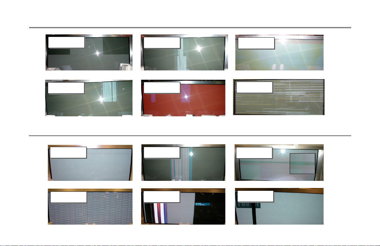
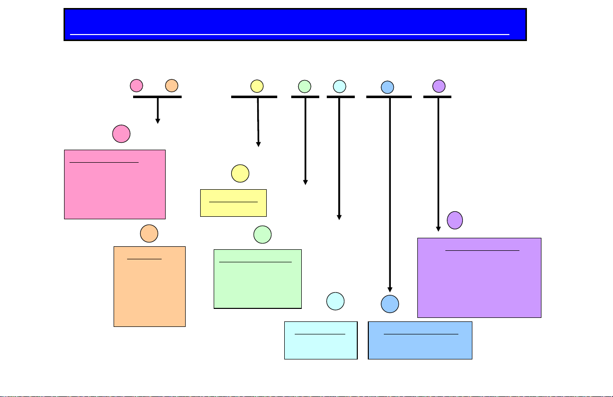
60’’ Known Visual problems with boards that fixed
Visual repair Index
Page # 37
Page # 37
Control Board & Y-Driver Amp
Page # 40
Page # 40
Y-Driver Top
Page # 38
Page # 38
Y- Amp
Page # 41
Page # 41
Control Board
60’’ Known Visual problems with boards that fixed
Page # 43
Page # 43
Y-Driver - Top
Page # 46
Page # 46
Page # 44
Page # 44
VSC- Board
Page # 47
Page # 47
Page # 39
Page # 39
Y-Driver Amp
Page # 42
Page # 42
X-Board upper right
Page # 45
Page # 45
Y-Driver - Top
Page # 48
Page # 48
VSC- Board
X- Board ( Top Right)
Y-Driver amp and X-Drive Top
2
Page 3
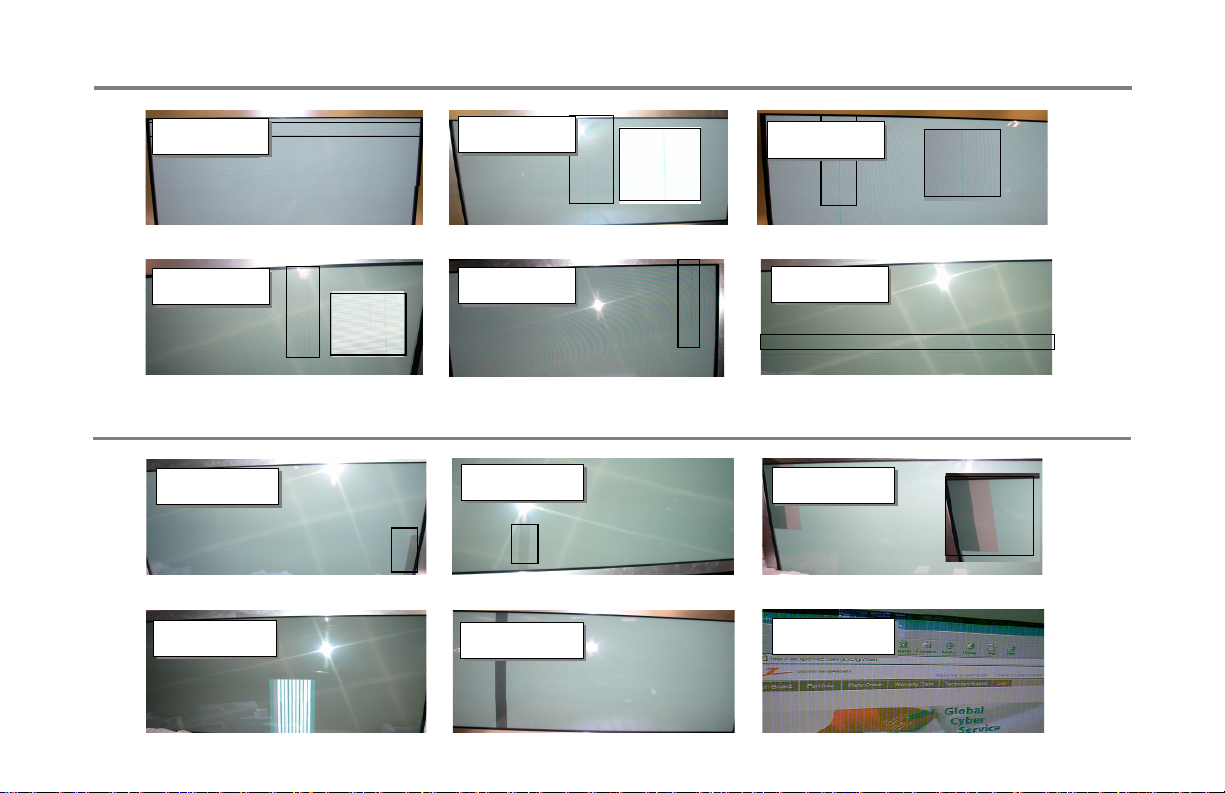
50’’ Known Visual problems with boards that fixed
Visual repair Index
Page # 49
Fig # 13
Page # 49
Fig # 13
Y-Driver Amp upper
Page # 52
Page # 52
VSC Board
Page # 50
Page # 50
Control board
Page # 53
Page # 53
X-Board upper right
50’’ Known Visual problems with boards that fixed
Page # 56
Page # 55
Page # 55
X- Board ( Lower Right)
Page # 58
Page # 58
Page # 56
X- Board ( Lower Left)
Page # 59
Page # 59
Page # 51
Page # 51
Control Board
Page # 54
Page # 54
Y- Driver Amp bottom
X- Board ( Bottom Left)
Page # 57
Page # 57
Control Board
Page # 60
Page # 60
Y- Driver Bottom
Y- Driver Amp and X-Drive Top
Control Board
3
Page 4
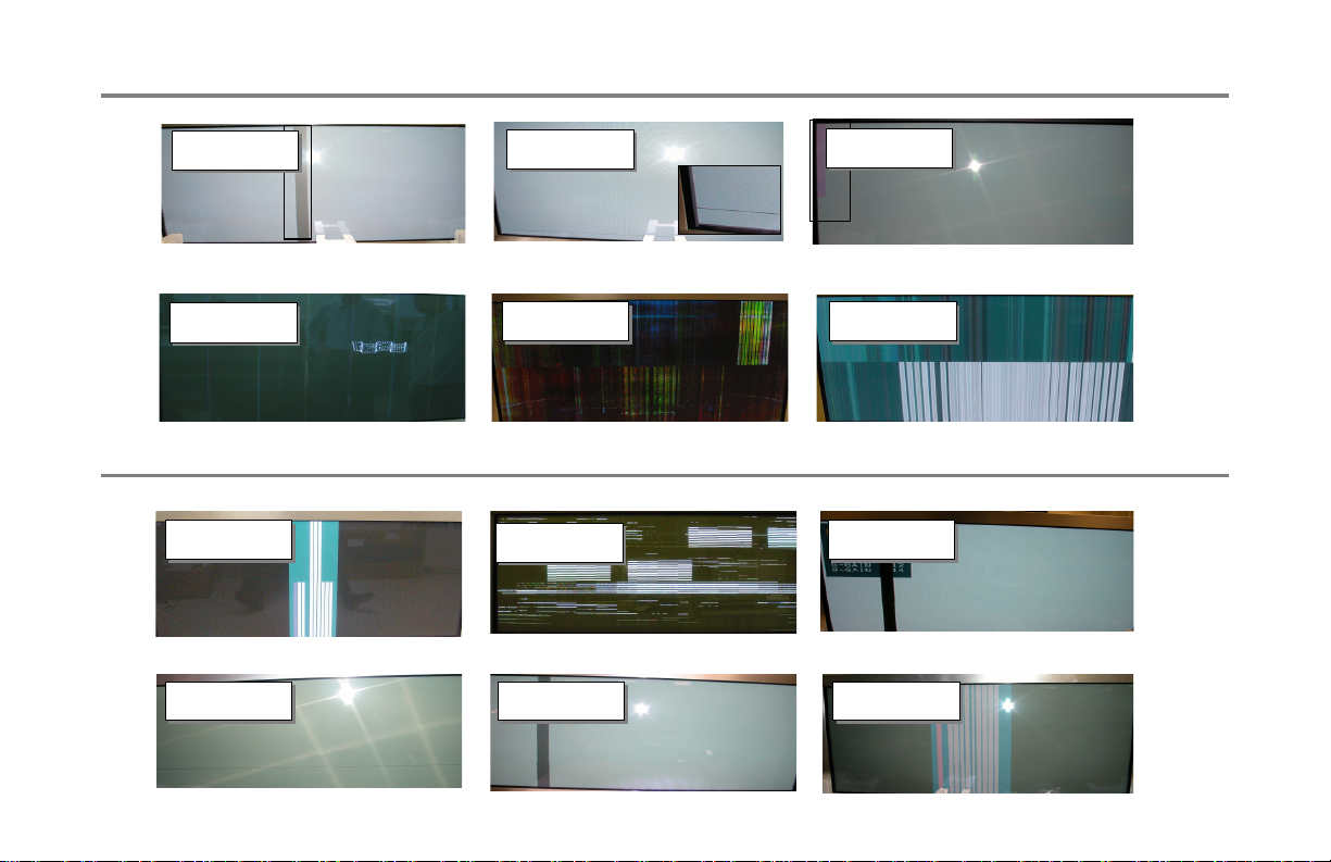
42’’ Known Visual problems with boards that fixed
Visual repair Index
Page # 61
Page # 61
Data @ X-Board – Yes/ tested for shorted
FOC IC – Ribbon shorted/ Defective Panel
Page # 64
Page # 64
Display’s waves - VSC
Page # 62
Page # 62
Installed Y- Driver Amp bottom no
Change/ Defective Panel
Page # 65
Page # 65
42’’ Known Visual problems with boards that fixed
Page # 67
Page # 67
Y-Driver - Top
Page # 70
Page # 70
Page # 68
Page # 68
VSC- Board
Page # 71
Page # 71
Page # 63
Page # 63
Data @ X-Board – Yes/ tested for shorted
FOC IC – Ribbon shorted/ Defective Panel
Page # 66
Page # 66
Y-Driver - TopY-Driver - Top
Page # 69
Page # 69
Y-Driver - Top
Page # 72
Page # 72
Y-Driver Amp upper
Control BoardControl board
4
Page 5
8QGHUVWDQGLQJ0RGHO1XPEHUVIRU/*'LVSOD\’V
08– 3=9
352'8&77<3(
• 00RQLWRU
• '%,'LJLWDO7XQHU
• .%,'9'
• 5%,$QDORJ7XQHU
• 7%,395
5(*,21
• 81$PHULFD
• =(XURSH
• 71(8
• 36$PHULFD
• --DSDQ
• 1.RUHD
'LVSOD\6L]H
,QFKHV
63(&,$/237,21
',63/$<'(9,&(
33'3
//&'
))ODW&57
60LFUR'LVSOD\
$VSHFW5DWLR
• =<;…ZLGH
• $%&…
(QJLQHHULQJ7RRO
)RUPDQXIDFWXULQJ
SXUSRVHRQO\
++LJK$OWLWXGH
93LYRW9HUWLFDO'LVSOD\
0+LJK$OWLWXGH3LYRW
4+RPH6HFXULW\1HWZRUN
''/3
//&'
5
Page 6

Introduction to Plasma
How the power supply works
Voltages for VS: Supplies support to the Y-Amplifier for
horizontal grid voltage. If the required voltage is not + or –
3% you may see the following in the picture: lines from side
to side or left to right, half picture top or bottom, intermittent
shutdown or dead.
Voltages for VA: Supplies support to the Z-Amplifier for
vertical grid voltage. If the required voltage is not + or – 3%
you may see the following in the picture: Comets, washout,
bleeding, intermittent shutdown or dead.
To start to understand plasma one must look for why this
voltage is not within specifications. In LG – Zenith line of
plasmas there are several power supply set-ups as follows:
60” plasma is made-up of a primary and secondary power
supply followed by a DC to DC converter. This is to support
the massive current that’s required to sustain picture
quality.
The 50” and 42” plasma power supplies are consolidated
into one board. In the 60” anyone of the three parts could
be out of adjustment. In the fifty and forty two the voltages
need to be still verified in chronological order. In most
cases if your facing a dead set scenario this is caused by
a shorted Y or X-driver board.
Testing for defective Y-drive boards can be done by looking
for a voltage drop if this is located in the Y-sustain
disconnect power and remove one Y-driver boards at a
time until Y-sustain voltage is accurate. If Y-sustain does
not respond with proper voltage supplied replace. Testing
for defective X-driver boards can be done by powering
down and disconnecting each X-driver and powering on
each quadrant at a time.
Pulse Frequency Coefficient: (PFC) adjustment is Located
the primary supply and is for aligning grid voltage. The
panels grid voltage averages 360 to 380 volts depending
on panel circuit.
Known symptoms:
No Power
Intermittent Power
Picture dimming to bright during certain seines
Primary colors off, Hue or flesh tones
Colors bleeding
Left to Right picture is dark to bright
Page 7
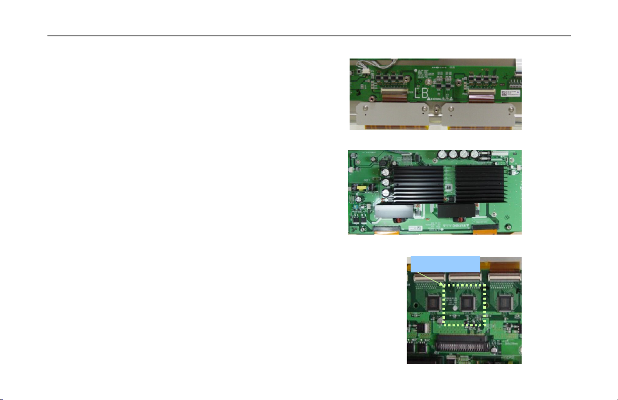
Introduction to Plasma
1. X B/D
Receiving LOGIC signal from CONTROL B/D to make ADDRESS
PULSE generating address discharge by an ON/OFF operation,
and supplies this waveform to COF IC (data) or ribbon IC.
X B/D
X B/D
2. Z sustain B/D
Responsible for making SUSTAIN PULSE and ERASE PULSE that
that generates SUSTAIN discharge in panel by receiving LOGIC
signals the CONTROL B/D.
The Sustain discharge waveform is supplied to panel through FPC (Z
B/D).
Composed of IPM,FET,DIODE, electrolytic capacitor, E/R coil.
3. Y drive B/D
1) This is a path to supply SUSTAIN ,RESET waveform which is made
from Y SUSTAIN B/D to panel through SCAN DRIVER IC.
2) Supplies the waveform that selects Horizontal pulse (Y SUSTAIN pulse) sequentially.
- Potential difference is 0V between GND and Vpp of DRIVER IC in SUSTAIN period.
- Generated potential difference between GND and Vpp only in SCAN period.
• E/R (Energy recovery)
• COF (Chip On Film)
• IPM (Intelligent Power Module)
Z B/D
Z B/D
Y SUB--
Y SUB
AMP B/D
AMP B/D
Scan drive IC
Page 8
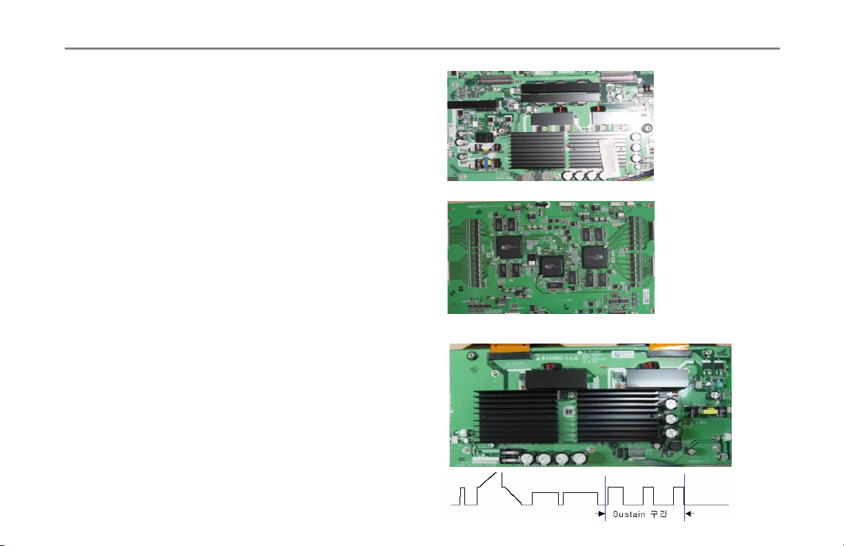
Introduction to Plasma
4. Y sustain B/D
Generates SUSTAIN, RESET waveform, VSC (SCAN) voltage
and supplies it to the Y DRIVER B/D.
Composed of IPM, DIODE, electrolytic capacitor, FET.
AMP B/D
YY--AMP B/D
5. Control (logic) Board
Creates signal processing (Contour noise, reduction ISM,..)
and an order of many FET switching IC’s on/ off of each
DRIVER B/D with R,G,B to each 8bit input COF ribbon IC.
Supply voltages 3.3V/ 5V.
6. IPM (Intelligent Power Module)
Connected to Z B/D and Y B/D, making Sustain waveform.
Sustaining and supplying a square wave to panel, creating video.
Composition
CAPACITORS/ DIODES/ IC LINEAR/ RESISTORS,
TRANSISTORS and FETS.
• E/R (Energy recovery)
• IPM (Intelligent Power Module)
DIG CONTROL B/D
DIG CONTROL B/D
Z-APM B/D
Page 9
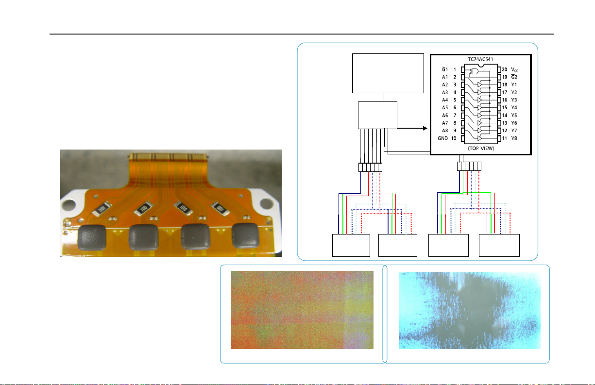
Introduction to Plasma
7. Ctrl B/D
CTRL B/D supplies video signal to COF. So if there is a
bar defect on panel this may be the ctrl b/d creating this
problem.
Flow, address signal
In the figure to the right shows data path to COF IC In this
description you can see how missing data can affect the
panel.
8. Checking order
1. Confirm Y, Z SUS signal cable.
2. Check Y DRV IC FAIL
3. Check Y sus b/d voltages (-Vy.Vscw)
4. Check Y ,Z-SUS IPM fail
5. Replace CTRL b/d
A. Mal-discharge problem Y-drive, Z -b/d.
<Diagram of ctrl b/d>
$6,&
Buffer
IC
$UUD\
UHVLVWRU
Each 16
lines
&2),& &2),& &2),& &2),&
B. Check VA and VS Voltage if occurred.
Page 10
Introduction to Plasma
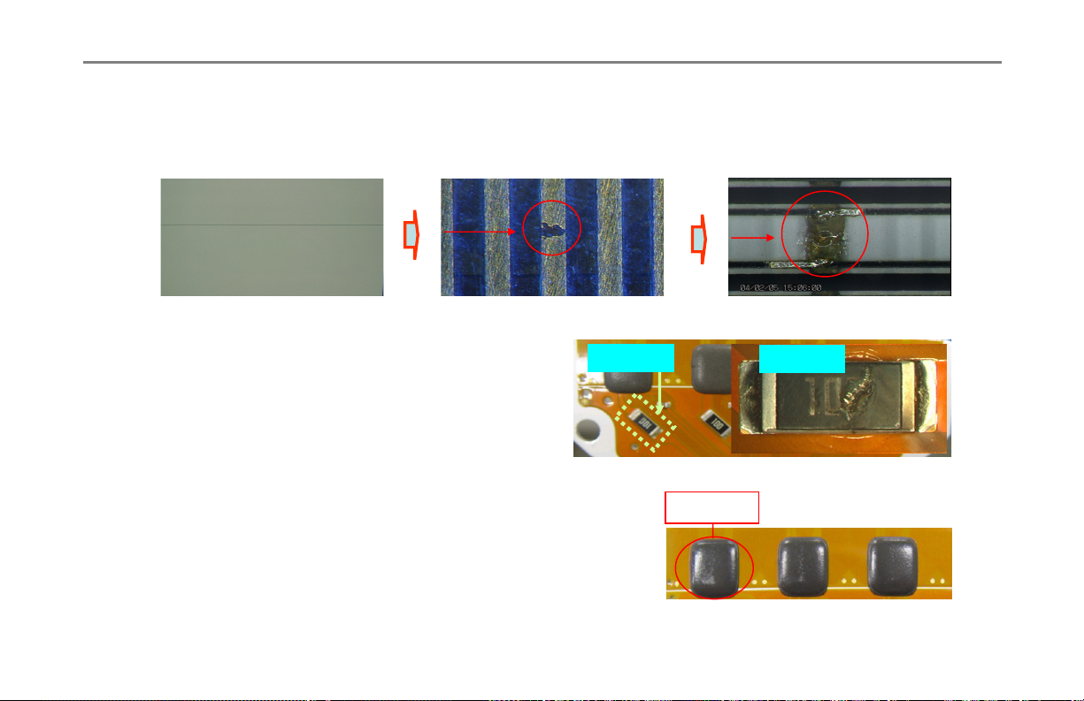
9. Check FPC
In case of horizontal 1 or more line, it is due to FPC or panel inside .ctrl b/d, Y b/d is just normal. First , clean the FPC
electrode with a cloth to clean off the ribbon connection removing particles.
Horizontal line.
COF ribbon to panel open Cell/ break down
10. Checking address COF input of resistor and IC
COF resistor check
Ⴇ
Check the both side of resistor With Digital multi meter(DMM) .
If the resistor is okay, the resistor value should be 10വif open
replace resistor.
Resistor
11. COF (Chip On Film)
Supplied with the X B/D waveform to the panel, controls grid & zones by
switching on or off the 96 pin COF IC.
the higher the resolution, the less spare space on the IC.
• E/R (Energy recovery)
• COF (Chip On Film)
• IPM (Intelligent Power Module)
Open
COF IC
Page 11
Introduction to Plasma
Vertical defect (line)
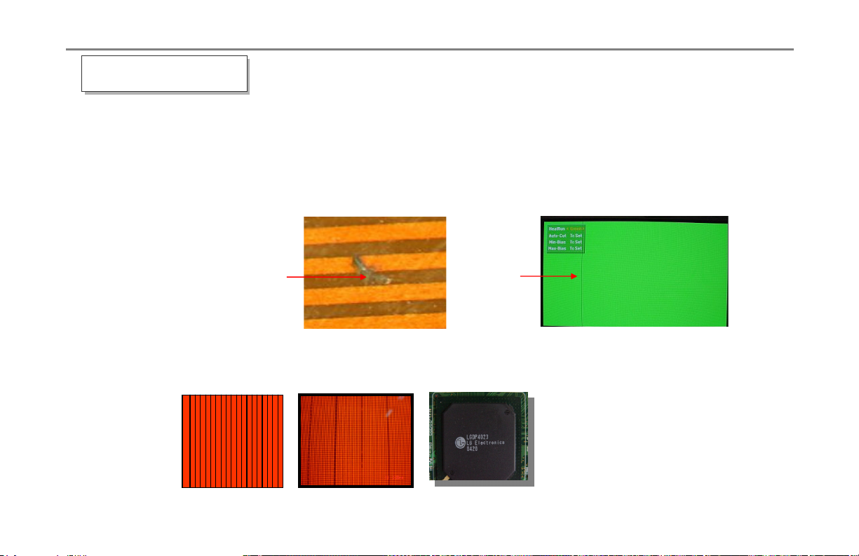
,QFDVHRIYHUWLFDOOLQHRUVKRUWFKHFNIRUIRUHLJQVXEVWDQFHVRQ&2)FRQQHFWRU
)LUVWFOHDQRIIWKHFRQQHFWRUZLWKFOHDQFORWKWRUHPRYHIRUHLJQ VXEVWDQFHV7HVWDJDLQWKHQLIWKHVDPH
OLQHDSSHDUVFKHFNIRUVKRUWHG,&6+257('UHSODFHSDQHO
1 line open or short
This phenomenon is due to COF IC inside short or adherence part of the Film and rear panel electrode
problem. In this case, replace the panel.
1 electrode open
Line open or short with same distance.
This is an ASIC of Ctrl b/d defect. ASIC defective, replace the ctrl b/d.
Will cause
1 line open
'$'DWD$UUDQJHU,&
Page 12
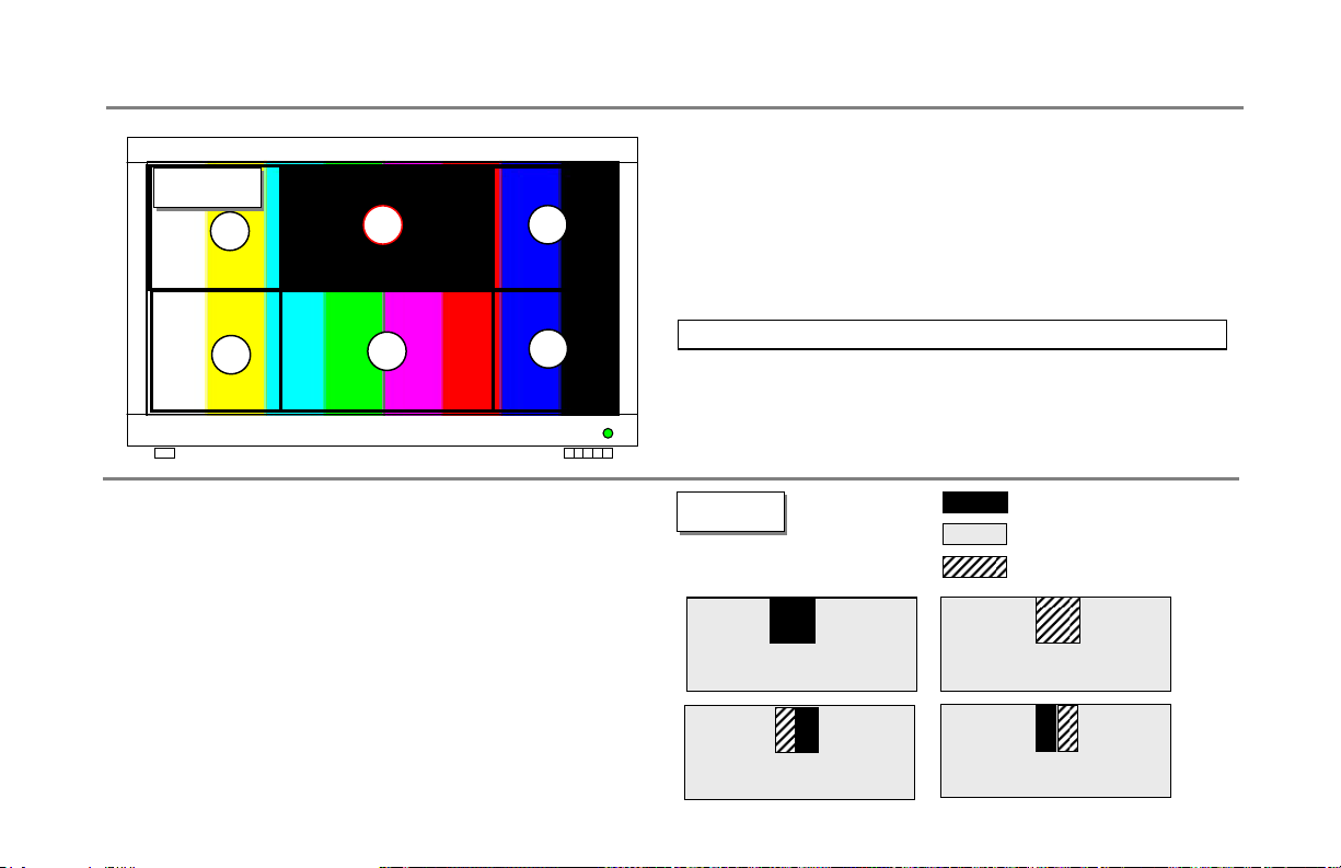
No image in the specific area (see the screen location 2)
1) Check the related X-Board’s power connector.
2) Check the signal cable between Controller PCB & X-Board.
Fig # 01
Fig # 01
1
4
2
2
5
3
6
3) Replace X-Board
Correlation between screen & X Boards
Screen Location X Board
1) Top left 3/10 l X Top-right / Bottom-left B/D
2) Center top 2/5 l X Center Top B/D
3) Top right 3/10 l X Top-left / Bottom-right B/D
4) Bottom left 3/10 l X Top-left / Bottom-right B/D
5) Center bottom 2/5 l X Center Top B/D
6) Bottom right 3/10 l X Top-right / Bottom-left B/D
Visual Troubleshooting
2. Known Tips as to no data and partial display
No image/ Data COF IC.
1) Caused by X Board’s having no power or connections.
Data COF is totally or partially not displayed
2) Check the connector between COF IC & X-Board.
3) Data COF IC is defective, replace the related X-Boards.
12
Fig # 02
Fig # 02
Examples,
Non-image
Non Image white
Partially displayed
Page 13
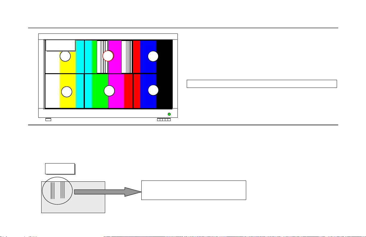
Regular vertical line with one or more Data COF IC
1) Check the related X Board’s power connector.
Fig # 03
Fig # 03
1
4
1) This is caused by X Board output IC being defective. When COF ICs have data this means the data transfer between the
Controller PCB and X Board is missing.
2) Check all related X Board connections.
3) Replace that X Board or CTRL PCB or both if needed.
Fig # 04
Fig # 04
2
5
3
6
Partial error or total error with One or more
ICs are defective.
2) Check the signal cable between Controller PCB & X-Board.
3) Replace X-Board
Correlation between screen & X Boards
Screen Location X Board
1) Top left 3/10 l X Top-right / Bottom-left B/D
2) Center top 2/5 l X Center Top B/D
3) Top right 3/10 l X Top-left / Bottom-right B/D
4) Bottom left 3/10 l X Top-left / Bottom-right B/D
5) Center bottom 2/5 l X Center Top B/D
6) Bottom right 3/10 l X Top-right / Bottom-left B/D
Visual Troubleshooting
13
Page 14
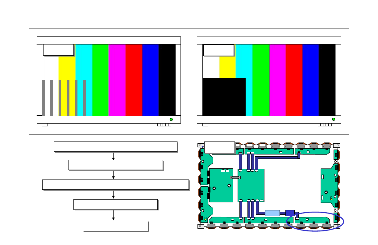
Address Bar ( Vertical ) & partial no-picture
Visual Troubleshooting
Fig # 05
Fig # 05
Related X-Board power supply voltage check
Related X-Board power supply voltage check
Related X-Board Connector check
Related X-Board Connector check
Related X-Board & Controller Board Connector check
Related X-Board & Controller Board Connector check
Related X-Board replacement
Related X-Board replacement
Module (Panel ) check
Module (Panel ) check
14
Fig # 06
Fig # 06
Bottom left 3/10 of the screen with no-pictureBottom left 3/10 of the screen with vertical bar
Fig # 07
Fig # 07
Y- Board
VR 424
B61 (TP;sus_up)
VR 301
Controller
Board
VSC
Board
P200
Side A/V L/F
Z- Board
VR 301
B61
(TP;sus_out)
Page 15
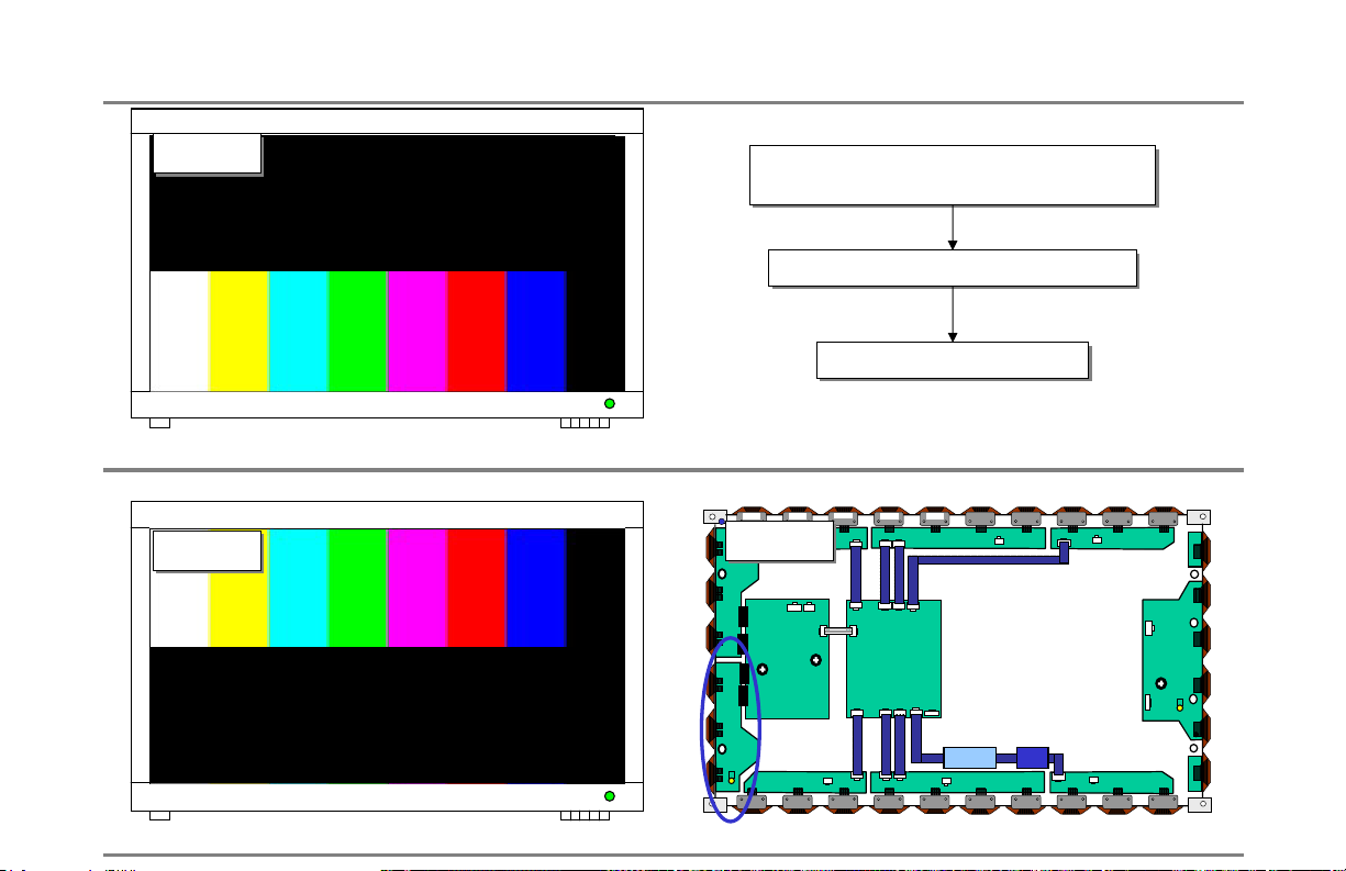
Bar (Horizontal) half -picture
Fig # 08
Fig # 08
2QO\ERWWRP,PDJHLV'LVSOD\LQJ
Fig # 09
Fig # 09
Visual Troubleshooting
<%RDUG<'ULYH%RDUG&RQQHFWRUFKHFN
<%RDUG<'ULYH%RDUG&RQQHFWRUFKHFN
Y-Drive Board ( Top ) Drive IC check
Y-Drive Board ( Top ) Drive IC check
Y-Drive Board replacement
Y-Drive Board replacement
Fig # 10
Fig # 10
Controller
Board
VSC
Board
P200
Y- Board
VR 424
VR 301
Z- Board
VR 301
B61
(TP;sus_out)
2QO\WRS,PDJHLV'LVSOD\LQJ
15
B61 (TP;sus_up)
Side A/V L/F
Page 16
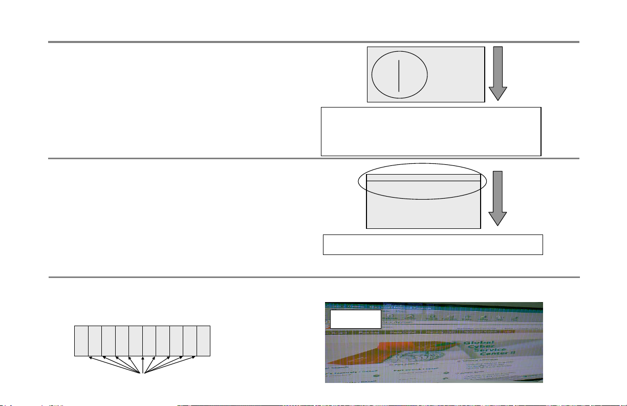
Vertical Lines
Visual Troubleshooting
6. One or more vertical lines in the screen.
1) Irregular vertical line is not related to Controller PCB or X Board.
2) It is mainly caused by the followings open (or short).
- Panel itself defect
- DATA COF FPC attached to panel is open or short.
- DATA COF attached to panel itself is defective
There can be several lines in ¼ inch wide area.
It can be seen on the both side, right and left.
The area is sometimes over ¼ inch wide.
7. One or more horizontal lines in the screen.
1) Irregular vertical line is not related to Controller PCB or Y Board.
2) It is mainly caused by the followings open (or short).
- Y FPC connector ය reinsertion
- Open because of Y Driver Board’s connector dry joint ය
Y DRV Board replacement
- Panel itself is defective, Y FPC attached to panel itself
is open or short
There can be several horizontal lines
8. Regular vertical lines in the whole screen. (mainly in one specific color, regular line is flicking)
1) This problem is related to CONTROL PCB.
2) Replace CONTROL PCB
Fig # 11
Fig # 11
Regular vertical lines in the whole screen
16
Page 17
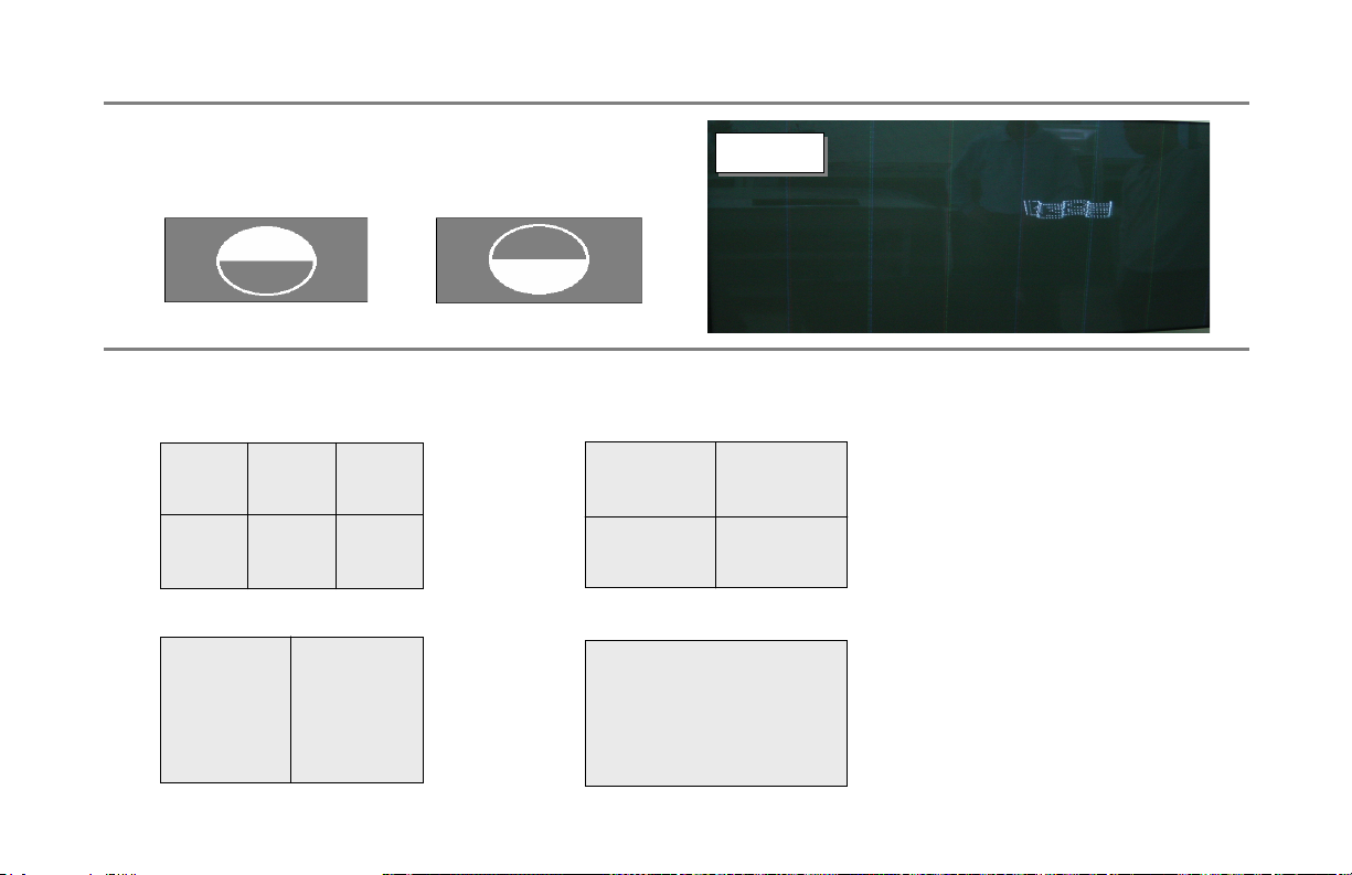
Vertical Lines
Visual Troubleshooting
9. Vertical Data copy
1) This happens when scan wave is not reproduced properly.
2) Replace Y-Board
<case 1 : partial Top copy > <case2 : partial Bottom copy >
10. Grid X and Y Layout by screen size.
60’’
X
X
Y
X
Y
50’’
40’’42’’
Fig # 46
Fig # 46
X
X
Y
Y
17
Page 18
Dark picture
Visual Troubleshooting
10. Input signal pattern is displayed but the screen is dark.
1) It happens when Z Board is not operating well.
2) Check whether Z Board’s power connector is plugged properly.
3) Check whether the signal connector between Controller PCB & Z Board is plugged.
4) Replace Z Board or controller PCB.
11. Input signal is white pattern but other colors are displayed in spots, missing data.
1) Check the slope & waveform of Y Board set up, set down.
2) Check the slope of Z Board’s ramp waveform
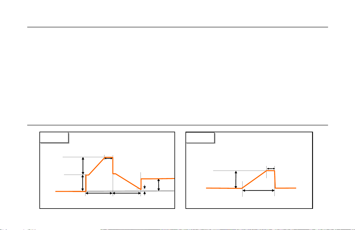
3) Measure each Board’s output waveform by over 200MHz scope and reference Fig. 12 and 13.
it is possible to control Y Board’s setup slope by adjusting VR2 and Z Board’s ramp slope by adjusting VR1.
Fig # 12
Fig # 12
Fig # 13
Fig # 13
- Y B/D measurement point : B61 ( SUS_UP OUTPUT ) - Z B/D measurement point : B61 ( SUS_OUT )
V-set-up
( 200V~240V)
Vs (170 ~ 185V)
0V
140ᓪ
< Y Sustain voltage wave>
20s5ᓪ
170s5ᓪ
VCC ( 90~110V)
10V
Vs (170 ~ 185V)
0V
3ᓪs2ᓪ
23ᓪ
< Z Ramp voltage wave >
18
Page 19
Dark picture at Top, Bottom or Center
Visual Troubleshooting
Fig # 14
Fig # 14
13. A specific brightness of one color is not clear.
1) Check CTRL Board’s input signal connector.
2) Replace CTRL Board.
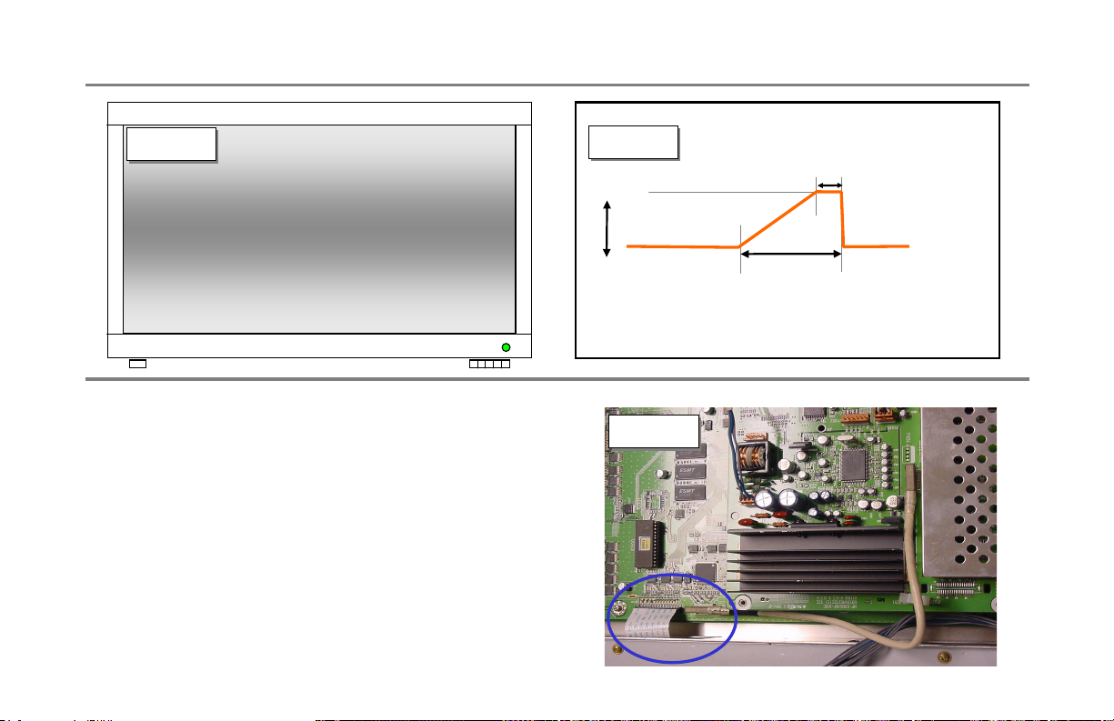
14. With a full white pattern, the picture is darker toward
the center.
1) Dark picture will occur when the Z-board is missing its ramp
waveform/ see Fig # 15
2) Check the connection between CTRL PCB and the Z-board
signal cable.
3) If the signal cable is -OK- Replace the Z-Board.
Fig # 15
Fig # 15
Vs (170 ~ 185V)
Fig # 16
Fig # 16
3ᓪs2ᓪ
23ᓪ
< Z Ramp voltage wave >
19
Page 20
No picture
1) Check CTRL PCB’s LED (D1~ D4).
2) Check the power or signal cable inputting into CTRL PCB.
3) Check X Board, Y Board and Z Board’s power connector.
4) Check the connector between CTRL PCB, X Board, Y Board, and Z Board respectively.
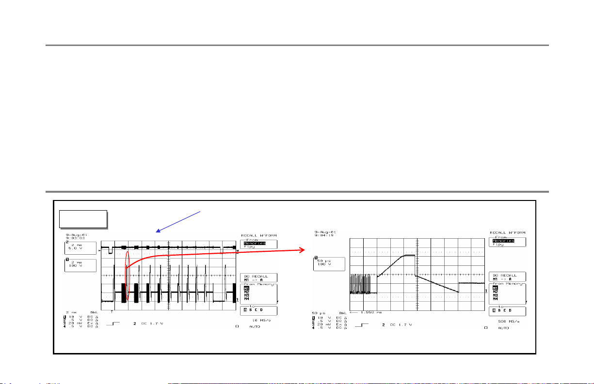
5) Measure Y Board’s output waveform with over 200MHz oscilloscope and compare it to Fig 17 below.
- Y Board measurement point : ( SUS_UP OUTPUT )
- X Board measurement point : ( SUS_DN OUTPUT )
6) Test data X Board waveform @ COF IC See Fig 34 page 26.
7) No Signal - Replace Controller PCB
V_SYNC
Fig # 17
Fig # 17
amplified
Visual Troubleshooting
< Y Board output wave - 1 Frame > < Y Board output wave (amplified) - 1 SF >
20
Page 21
Voltage Adjustment
Fig # 18
Fig # 18
TP5 GND
Service Adjustment
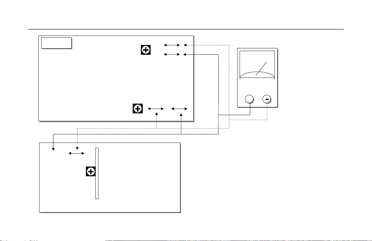
When replacing power board,
Be sure to follow Power Assembly voltage Proc.
<SMPS Board>
PFC +
PFC -
VR801
VS · 1V
PFC PACK
VA Adjust
VR8401
VS Adjust
VR8501
TP3
GND
TP6 VA
TP4
VS
21
DMM
+
+
1. PFC adjustment
-. Select 100% White Pattern signal and Pre-Heat panel.
-. Connect DMM with TP PFC+ and TP PFC – (GND).
-. adjust VR801 to 380V (within ·1V ).
2. VA adjustment
-. Connect DMM + terminal with P814 #1 Pin.
-. Turn VR8401 (VA) to adjust the voltage on DMM to VA voltage
value marked on label @ bottom- right of panel. (allowable tolerance :
·0.5V )
3. VS adjustment
-. Connect DMM’s + terminal with P803 # 9 Pin.
-. Turn VR 8501 (VS)to adjust the voltage with DMM to Vs voltage
value marked on label @ bottom- right of panel.
Page 22
Voltage Adjustment
Service Adjustment
Fig #47
Fig #47
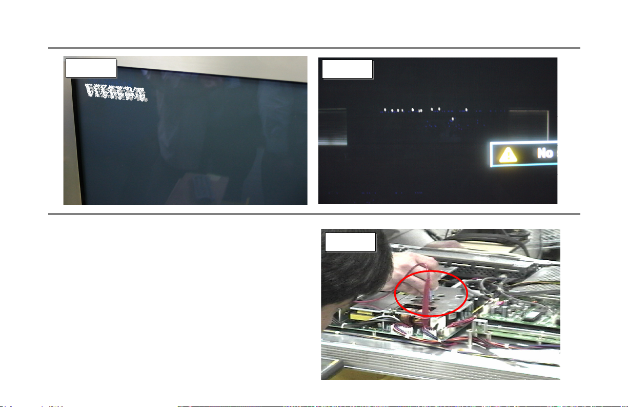
Problem: The picture above is an example of distorted
text.
Cure: VA & VS voltage adjustment is needed when
the following items are found:
• Distorted text
• Blocked text
• Pixilated picture
• Dots running from side to side
• Tearing in the picture
• Video smear
Fig # 48
Fig # 48
Fig # 49
Fig # 49
22
Page 23
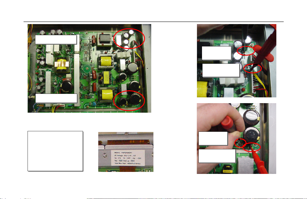
60’’ Test points and voltage adjustments.
VS adjustment
VS adjustment
VA adjustment
VA adjustment
Service Adjustment
VA adjust
VA adjust
VR8401
VR8401
VA test point
VA test point
TP-6
TP-6
The voltage settings
The voltage settings
change from model
change from model
to model and are
to model and are
labeled and located
labeled and located
at the top center of
at the top center of
the screen.
the screen.
23
VS adjust
VS adjust
VR8501
VR8501
VS test point
VS test point
TP-4
TP-4
Page 24
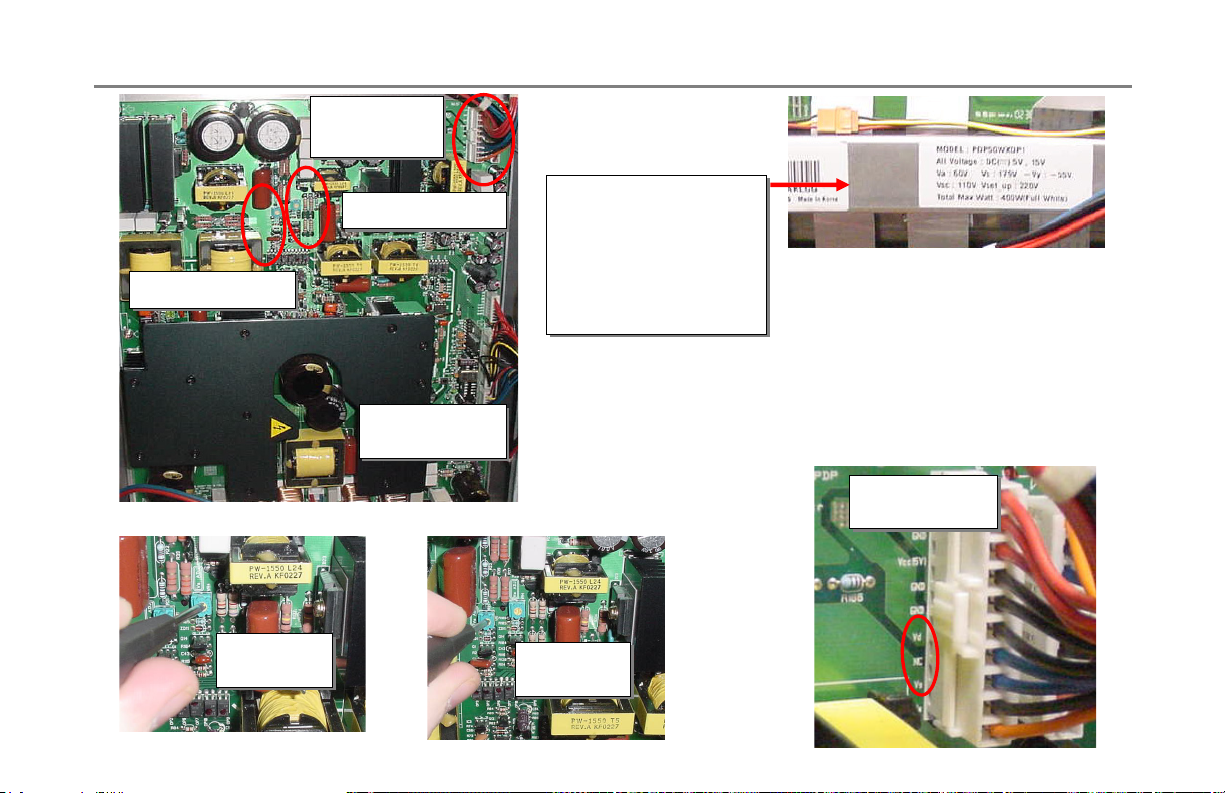
50’’- 26 series Test points and voltage adjustments.
VS/ VA
VS/ VA
Test Points
Test Points
The voltage settings
The voltage settings
change from model
change from model
to model and are
to model and are
labeled and located
labeled and located
at the top center of
at the top center of
VA adjustment
VA adjustment
VS adjustment
VS adjustment
the screen.
VS test point
VS test point
TP1
TP1
the screen.
Service Adjustment
VA test point
VA test point
VA adjust
VA adjust
RV601
RV601
VS adjust
VS adjust
RV401
RV401
24
Page 25
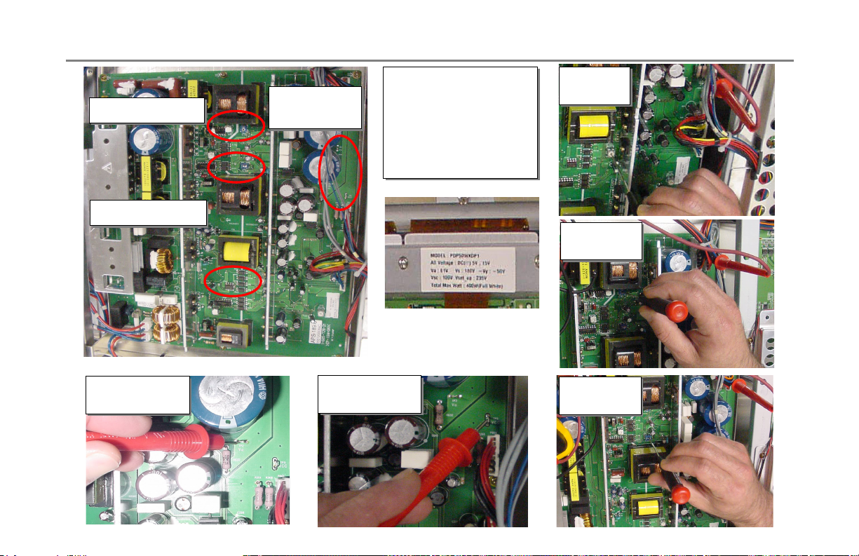
50’’- 28 Series Test points and voltage adjustments.
Service Adjustment
VS adjustment
VS adjustment
VA adjustment
VA adjustment
VA test point
VA test point
TP2
TP2
VS/ VA
VS/ VA
Test Points
Test Points
VS test point
VS test point
TP1
TP1
The voltage settings
The voltage settings
change from model
change from model
to model and are
to model and are
labeled and located
labeled and located
at the top center of
at the top center of
the screen.
the screen.
Five B +
Five B +
RV203
RV203
VS adjust
VS adjust
RV401
RV401
VA adjust
VA adjust
RV601
RV601
25
Page 26
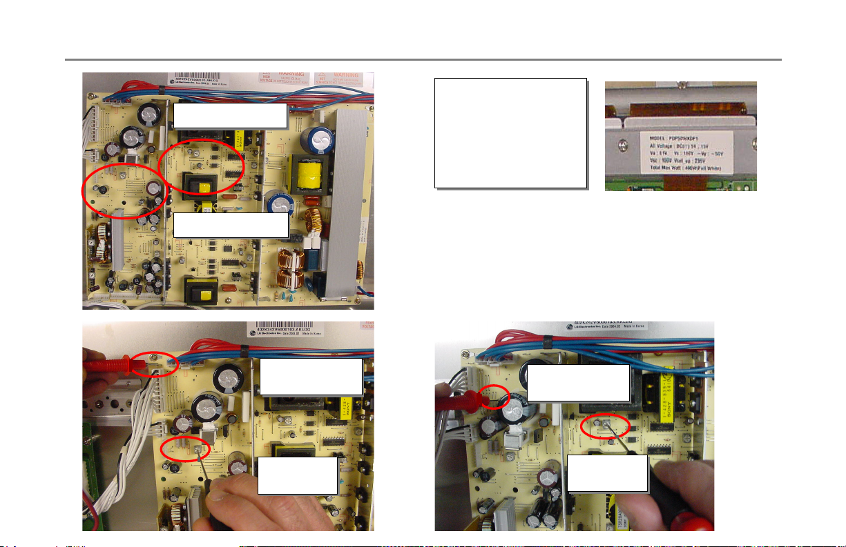
42’’ with tuner test points and voltage adjustments.
VS adjustment
VS adjustment
VA adjustment
VA adjustment
VS test point
VS test point
TP-2
TP-2
Service Adjustment
The voltage settings
The voltage settings
change from model
change from model
to model and are
to model and are
labeled and located
labeled and located
at the top center of
at the top center of
the screen.
the screen.
VA test point
VA test point
TP-1
TP-1
VS adjust
VS adjust
RV601
RV601
26
VA adjust
VA adjust
RV401
RV401
Page 27
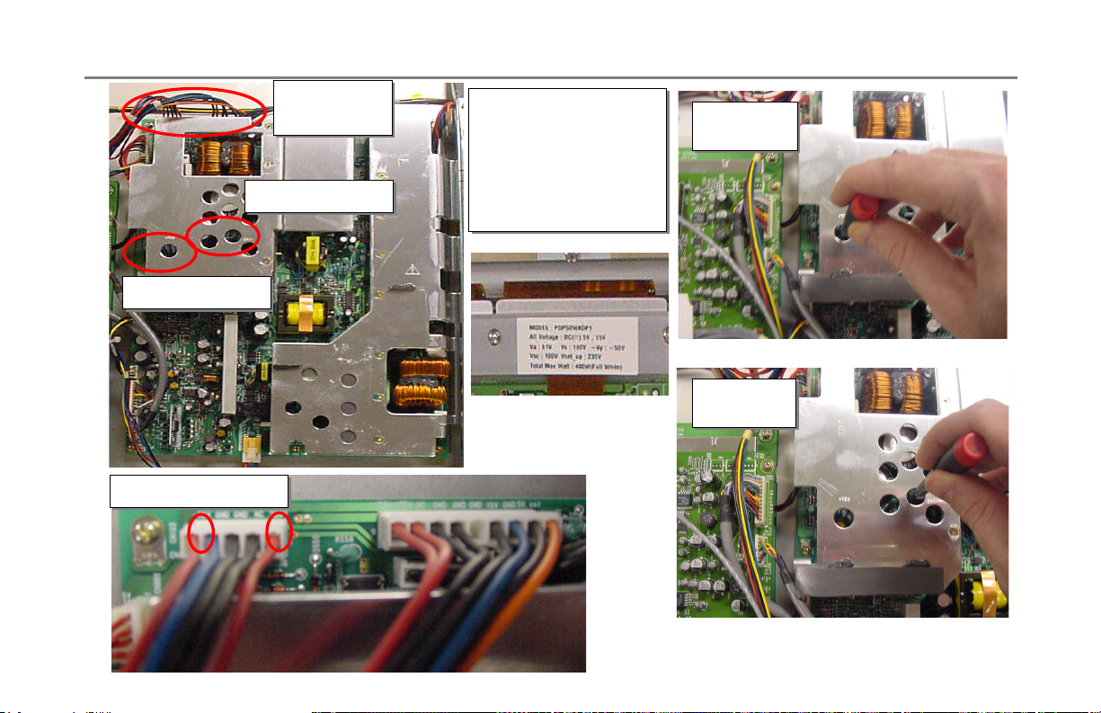
42’’ early model, Test points and voltage adjustments.
VS/ VA
VA adjustment
VA adjustment
VS adjustment
VS adjustment
VS/ VA test points
VS/ VA test points
VS/ VA
Test Points
Test Points
The voltage settings
The voltage settings
change from model
change from model
to model and are
to model and are
labeled and located
labeled and located
at the top center of
at the top center of
the screen.
the screen.
Service Adjustment
VA adjust
VA adjust
RV751
RV751
VS adjust
VS adjust
R671
R671
27
Page 28
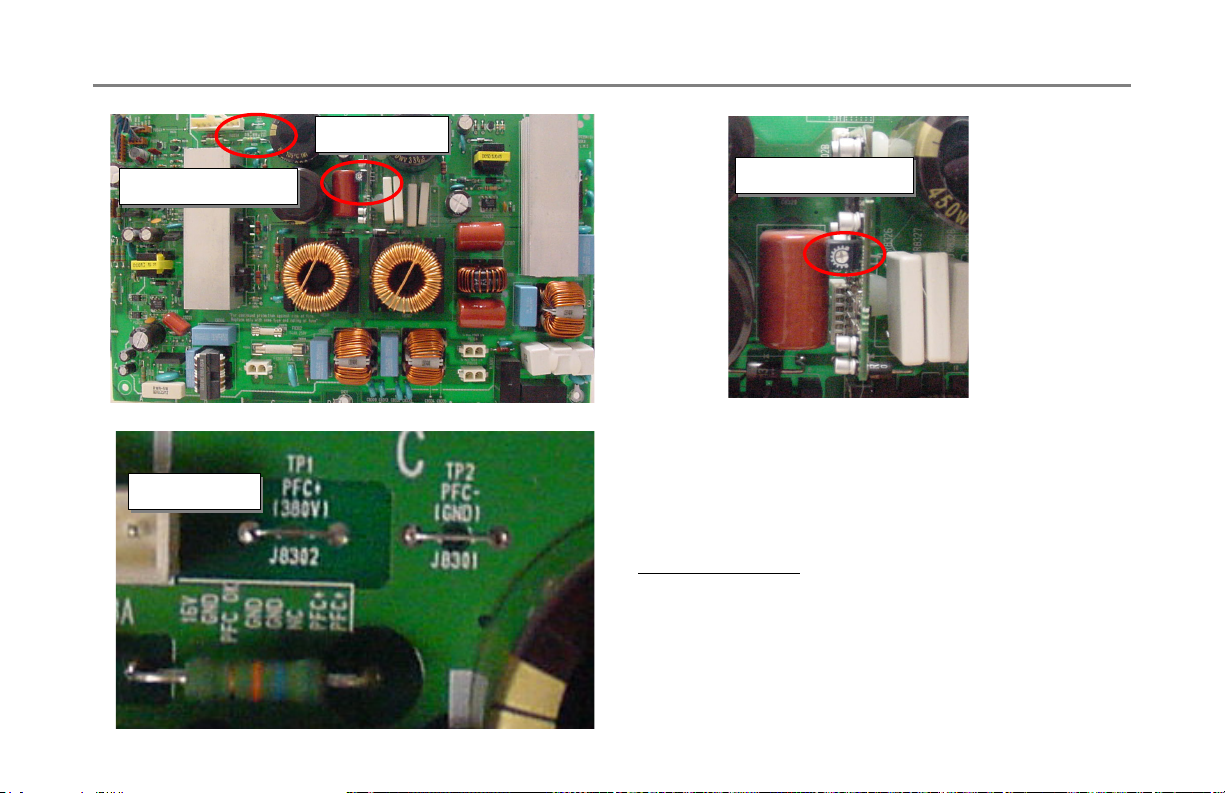
Primary power supply adjustment/ coefficient/ Example 60’’.
Test Points
Test Points
PFC adjustment
PFC adjustment
Pulse Frequency - Coefficient (PFC) adjustment is
Located the primary supply and is for aligning grid
Test Points
Test Points
voltage. The panels grid voltage averages 360 to
380 volts depending on panel circuit.
Service Adjustment
PFC adjustment
PFC adjustment
Known symptoms
1. Intermittent Power
2. Picture dimming to bright during certain seines
3. Primary colors off, Hue or flesh tones
4. Colors bleeding
5. Left to Right picture is dark to bright
:
28
Page 29
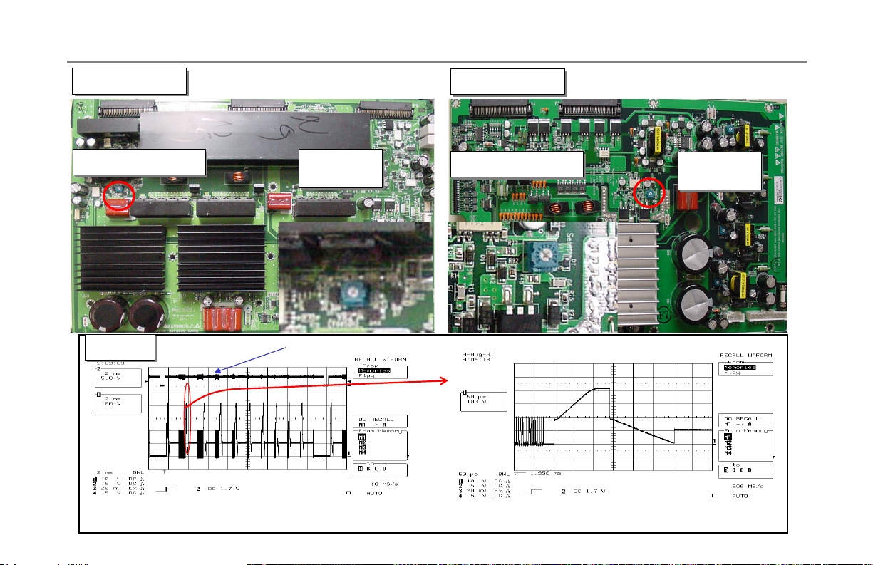
Y-amp, Test points and voltage adjustments.
Service Adjustment
6871QYH023A
6871QYH023A
Y- VA test points
Y- VA test points
Fig # 61
Fig # 61
/ Example 60’’
VA adjust
VA adjust
VR1
VR1
V_SYNC
amplified
6871QYH027A
6871QYH027A
Y- VA test points
Y- VA test points
/ Example 42’’
VA adjust
VA adjust
V Set-up
V Set-up
< Y Board output wave - 1 Frame > < Y Board output wave (amplified) - 1 SF >
29
Page 30
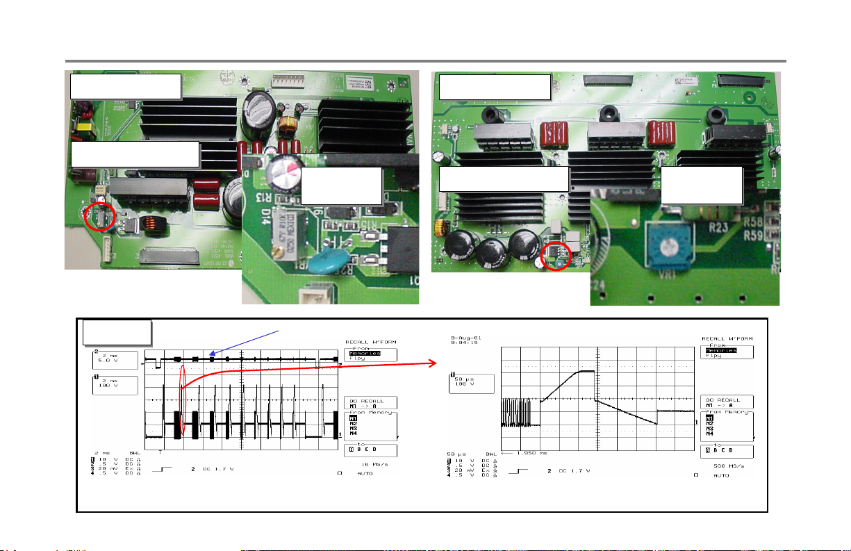
Z-Sus, Test points and voltage adjustments.
Service Adjustment
6871QZH020B
6871QZH020B
Z- VA test points
Z- VA test points
/ Example 50’’
Fig # 62
Fig # 62
VA adjust
VA adjust
VR1
VA adjust
VR1
VA adjust
VR1
VR1
V_SYNC
amplified
6871QYH027A
6871QYH027A
Y- VA test points
Y- VA test points
/ Example 42’’
VA adjust
VA adjust
VR1
VR1
< Y Board output wave - 1 Frame > < Y Board output wave (amplified) - 1 SF >
30
Page 31
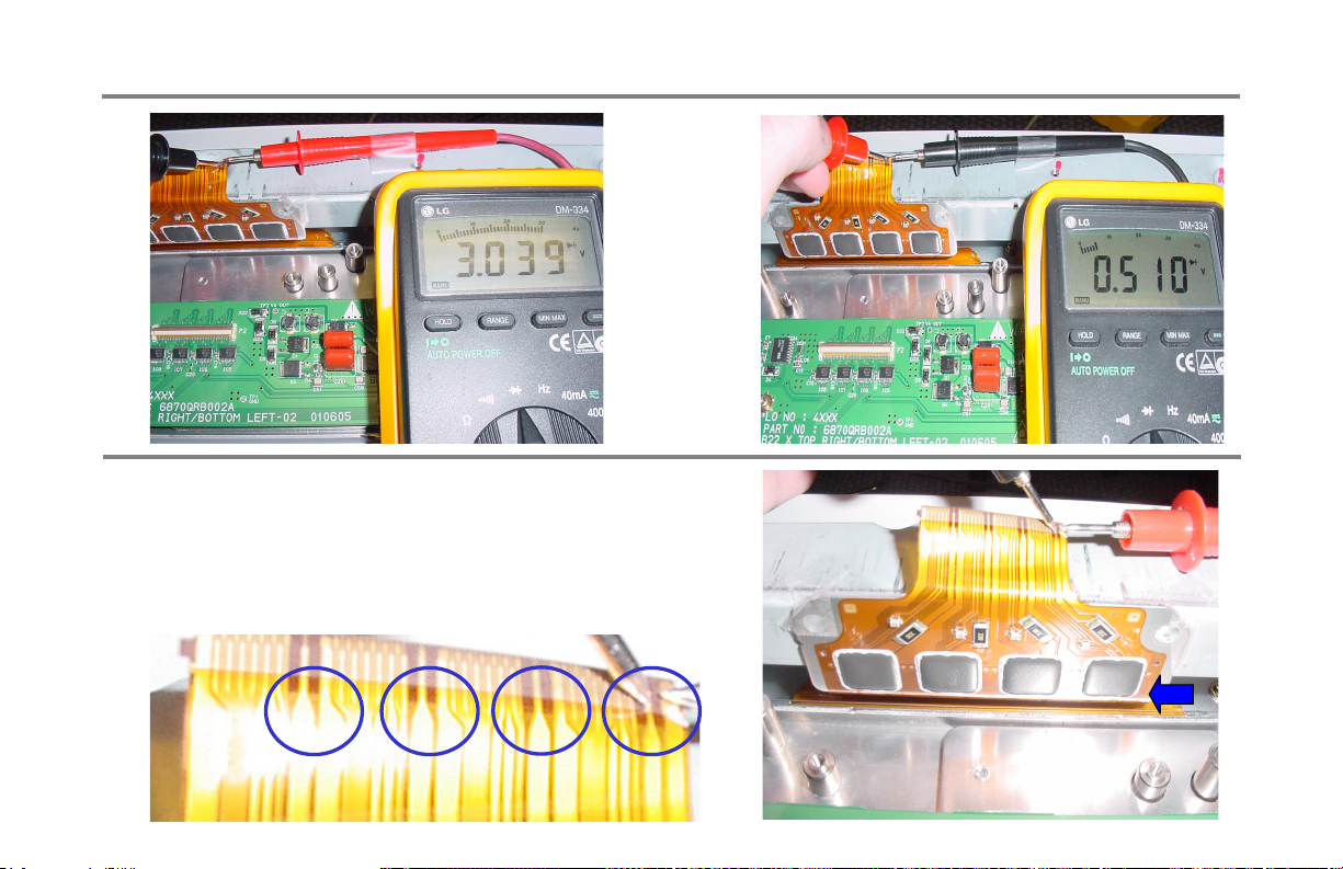
Testing COF IC for Defective Panel/ Example 50’’
If an X-Board is found defective there is a slim
possibility that the panel could cause the new X-Board
Installed to fail due to panel short test by performing
Diode Check as in the above figures.
Panel Testing
31
FOC IC
Page 32
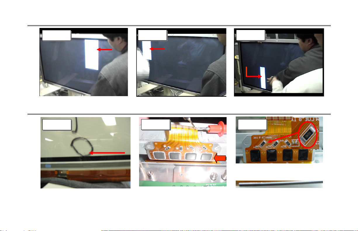
Defective Panel with shorted COF IC/ Example 50’’.
Panel Testing
Fig # 52
Fig # 52
Fig # 53
Fig # 53
Fig # 54
Fig # 54
Rotating Bar
Rotating Bar
If an X-Board is found defective there is a slim possibility that a pixel could be found defective in the
responsible quadrant. This is caused by an arch in the panel caused at the point of the IC’s failure.
Fig # 55
Fig # 55
The above FIGURE 55 shows the defective cell damage. Figure 56 shows the panel ribbon
attached to panel. We identified that for this panel the ribbons integrated IC was shorted.
Rotating Bar
Fig # 56
Fig # 56
COF IC
Fig # 57
Fig # 57
Open resistor
due to defective IC and panel
Note: In figure 55 is 1 defective cell this is caused by an arch in the panel, this caused COF IC too short.
32
Page 33
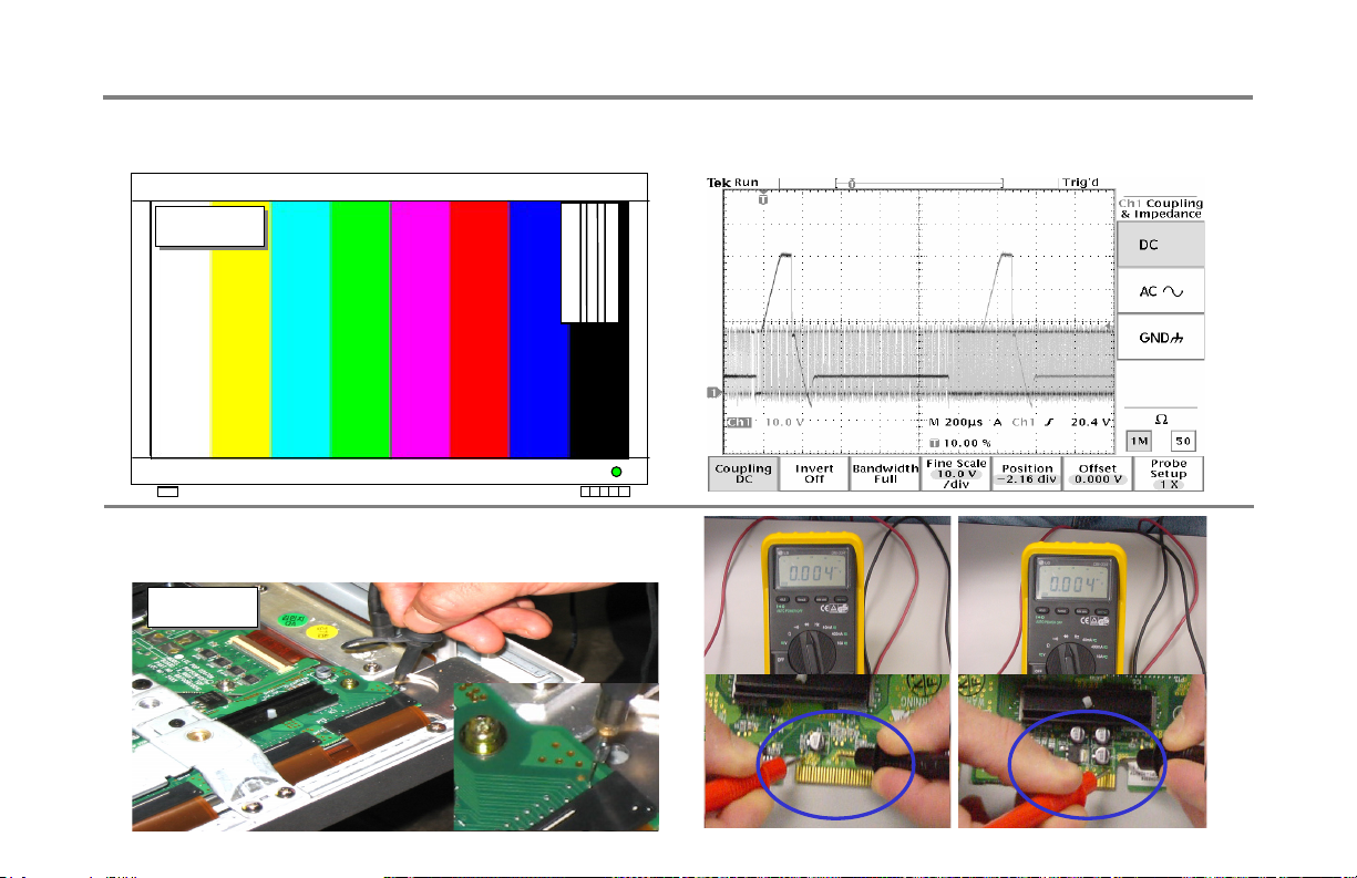
Testing Y driver board for problems/ Example 50’’.
1) Problem occurs when IC shorts and loss of signal to panel.
2) Check the con. between CTRL & Z Board’s signal cable. 5) Sustain-up Waveform example
Fig # 58
Fig # 58
3) The following image is the test point for waveform.
4) To the right is two test points for shorted IC’s 50’’.
Fig # 59
Fig # 59
Panel Testing
33
Page 34
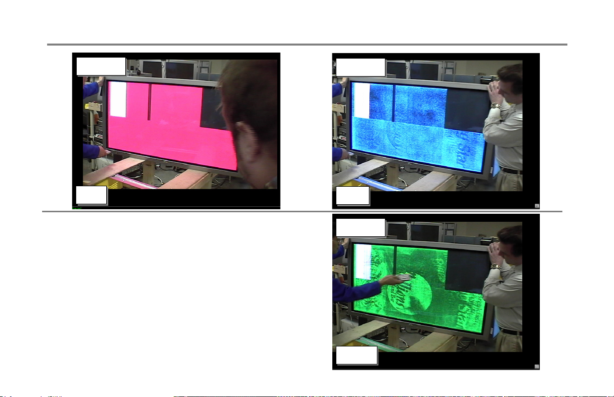
Defective Panel with excessive etching
Panel Testing
Fig # 49
Fig # 49
Red
Red
Most etching can be identified be using a Green/ Blue
or Red background and by adjusting the intensity
down. If the one color is displayed that CAUSED the
etching the color will be low in intensity compared to
the rest of the screen.
Etching considerations for extreme cases you need to
run white balance or heat run in 6 hour increments upto 24 hours. If you can’t perform a proper white
balance after 24 hours the panel is not within spec and
the panel will not work/ display properly.
Fig # 50
Fig # 50
Blue
Blue
Fig # 51
Fig # 51
Green
Green
34
Page 35
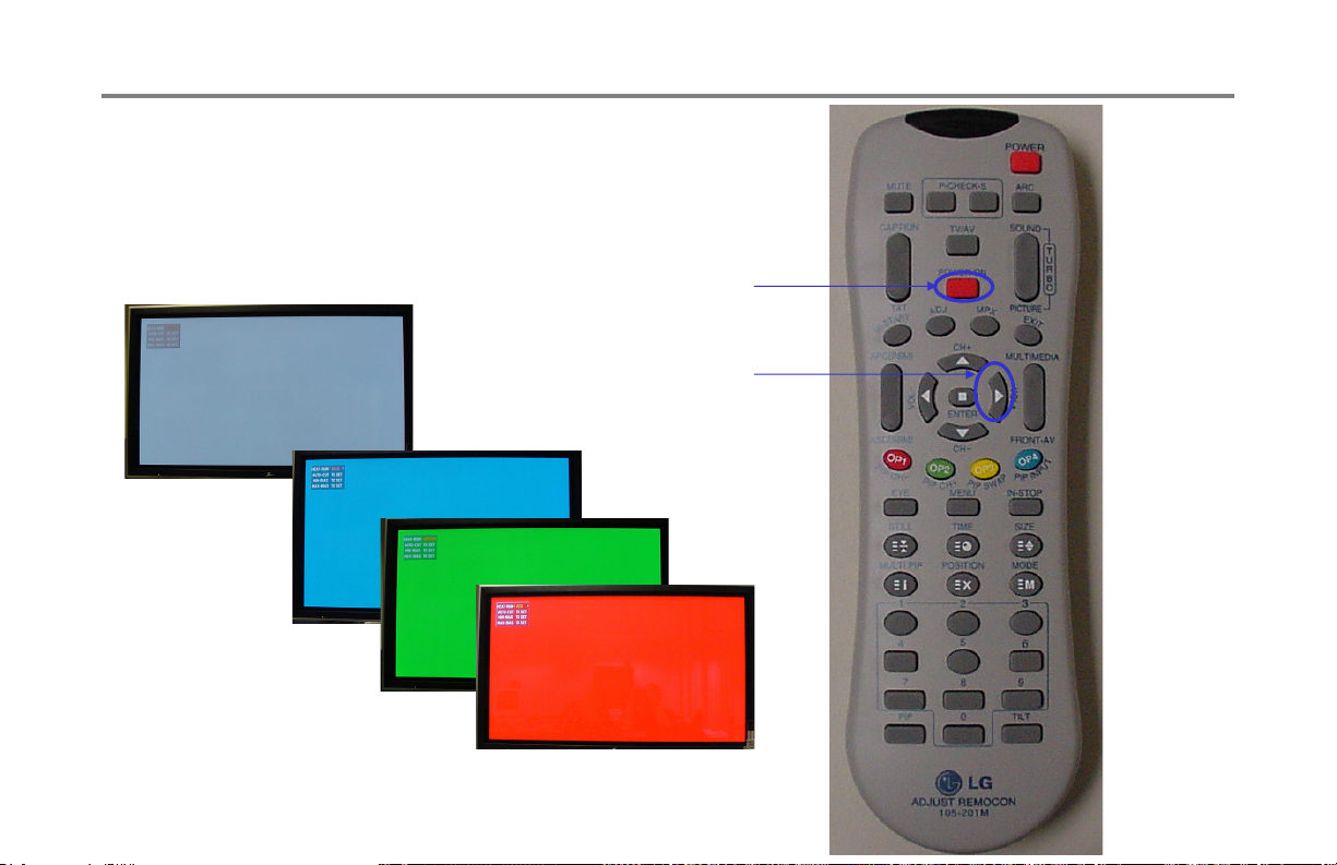
Etching Correction (Activating Heat Run) for Defective Panel
To enter in to White Balance (Heat Run), Press Power On (1).
Then, press adjust right (2) to activate Blue, Green and Red.
With the Heat run activated on White Balance run for 6 hours
and check color background by pressing adjust right (2) for
testing picture quality. Complete and repeat if needed not to
exceed 24 hours.
1
2
Panel Testing
35
Page 36
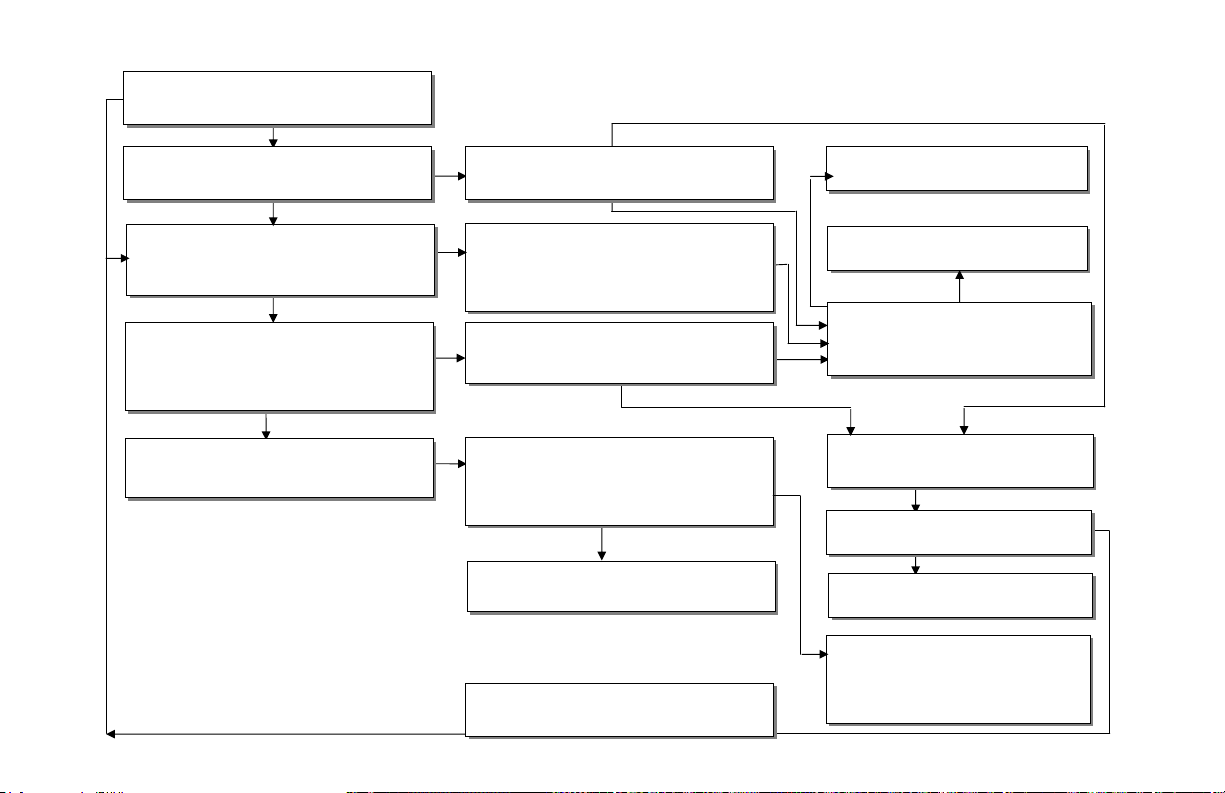
Troubleshooting
No
Does the LED on the front of the
Does the LED on the front of the
unit light with the A/C switch ON?
unit light with the A/C switch ON?
Yes
Check sources output by the SMPS.
Check sources output by the SMPS.
Is a source missing or low?
Is a source missing or low?
Yes
Unload the SMPS. Check for all of
Unload the SMPS. Check for all of
the output voltages from the SMPS.
the output voltages from the SMPS.
Are all of the voltages present?
Are all of the voltages present?
Yes
Reload the SMPS one connector at
Reload the SMPS one connector at
a time and test the output voltages.
a time and test the output voltages.
Do any of the voltages drop when
Do any of the voltages drop when
the connector is connected?
the connector is connected?
Yes
Replace the PWB associated with
Replace the PWB associated with
that shorted line.
that shorted line.
No
Does the power control line
Does the power control line
change at power ON?
No
No
No
No
change at power ON?
Yes
Check the connectors which would
Check the connectors which would
normally have V applied from the
normally have V applied from the
SMPS for shorts to ground. Do any
SMPS for shorts to ground. Do any
Does the power control line
Unload the PWB causing the
Unload the PWB causing the
shorted line and retest for the short
shorted line and retest for the short
on the same line. Does the short
on the same line. Does the short
Replace the suspected PWB.
Replace the suspected PWB.
shorts exist?
shorts exist?
Does the power control line
change at power ON?
change at power ON?
No
still exist?
still exist?
Yes
Yes
No
Power Section
No Picture
Replace the VSC PWB.
Replace the VSC PWB.
Replace the Control PWB.
Replace the Control PWB.
No
Check the Control PWB for
No
Check the Control PWB for
power function. Is power
power function. Is power
Do all the fans begin to turn?
Do all the fans begin to turn?
At power ON is 12V applied to
At power ON is 12V applied to
Replace the fan that is not
Replace the fan that is not
present?
present?
No
all of the fans?
all of the fans?
Yes
starting up.
starting up.
Yes
No
Check for 12V from SMPS.
Check for 12V from SMPS.
Is it present at Power ON?
Is it present at Power ON?
36
Replace the PWB associated
Replace the PWB associated
with that shorted line and
with that shorted line and
retest for any other shorts to
retest for any other shorts to
ground.
ground.
Page 37
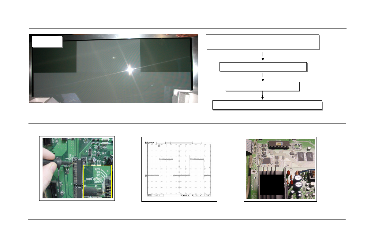
60’’ Known Visual problems with boards that fixed
Fig # 19
Fig # 19
Control Board & Y-Driver Amp
Visual Problems
Check & Adjust: PFC / VS / VA voltages to panel
Check & Adjust: PFC / VS / VA voltages to panel
specifications
specifications
Check Y-Sustain Sub-amp wave form
Check Y-Sustain Sub-amp wave form
Okay? Replace Y-Sustain Amp
Okay? Replace Y-Sustain Amp
Not Resolved? Replace Digital Control board
Not Resolved? Replace Digital Control board
Digital
Digital
Control
Control
v.s.c
Board
Y Sustain WF test point
Y Sustain WF
Digital Control board
37
Page 38
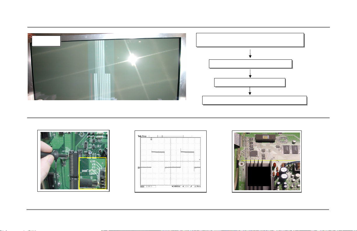
60’’ Known Visual problems with boards that fixed
Fig # 20
Fig # 20
Y- Amp
Visual Problems
Check & Adjust: PFC / VS / VA voltages to panel
Check & Adjust: PFC / VS / VA voltages to panel
specifications
specifications
Check Y-Sustain Sub-amp wave form
Check Y-Sustain Sub-amp wave form
Okay? Replace Y-Sustain Amp
Okay? Replace Y-Sustain Amp
Not Resolved? Replace Digital Control board
Not Resolved? Replace Digital Control board
Digital
Digital
Control
Control
v.s.c
Board
Y Sustain WF test point
Y Sustain WF
Digital Control board
38
Page 39
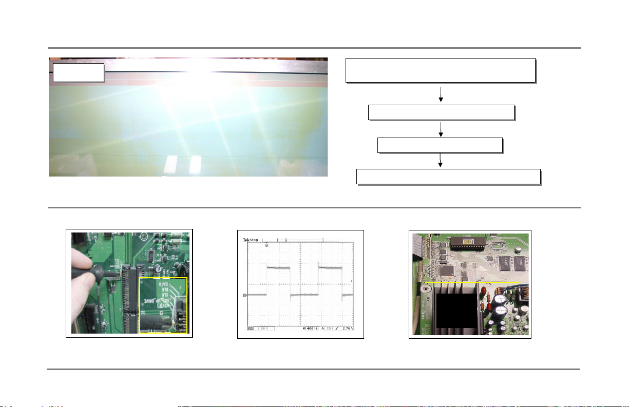
60’’ Known Visual problems with boards that fixed
Fig # 21
Fig # 21
Y-Driver Amp
Visual Problems
Check & Adjust: PFC / VS / VA voltages to panel
Check & Adjust: PFC / VS / VA voltages to panel
specifications
specifications
Check Y-Sustain Sub-amp wave form
Check Y-Sustain Sub-amp wave form
Okay? Replace Y-Sustain Amp
Okay? Replace Y-Sustain Amp
Not Resolved? Replace Digital Control board
Not Resolved? Replace Digital Control board
Digital
Digital
Control
Control
v.s.c
Board
Y Sustain WF test point
Y Sustain WF
Digital Control board
39
Page 40
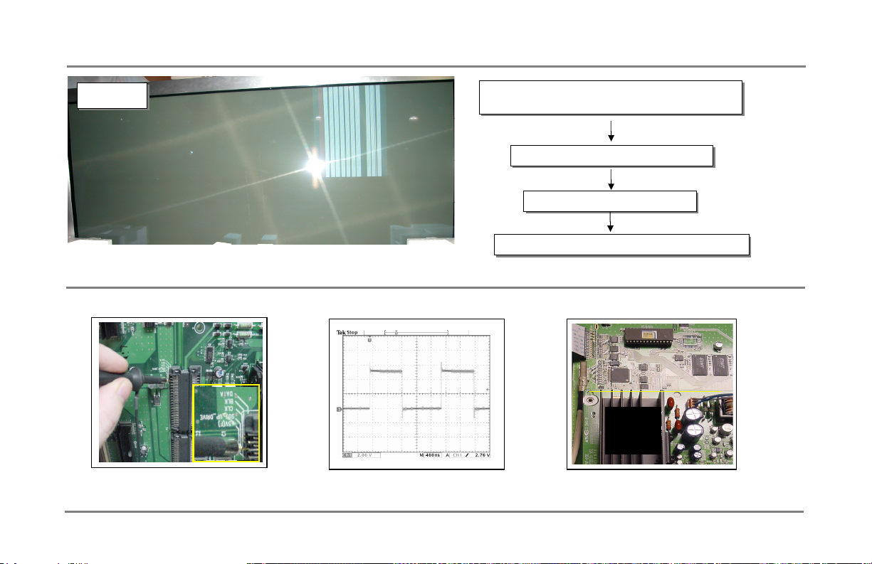
60’’ Known Visual problems with boards that fixed
Fig # 22
Fig # 22
Y-Driver Top
Visual Problems
Check & Adjust: PFC / VS / VA voltages to panel
Check & Adjust: PFC / VS / VA voltages to panel
specifications
specifications
Check Y-Sustain Sub-amp wave form
Check Y-Sustain Sub-amp wave form
Okay? Replace Y-Sustain Amp
Okay? Replace Y-Sustain Amp
Not Resolved? Replace Digital Control board
Not Resolved? Replace Digital Control board
Digital
Digital
Control
Control
v.s.c
Board
Y Sustain WF test point
Y Sustain WF
Digital Control board
40
Page 41
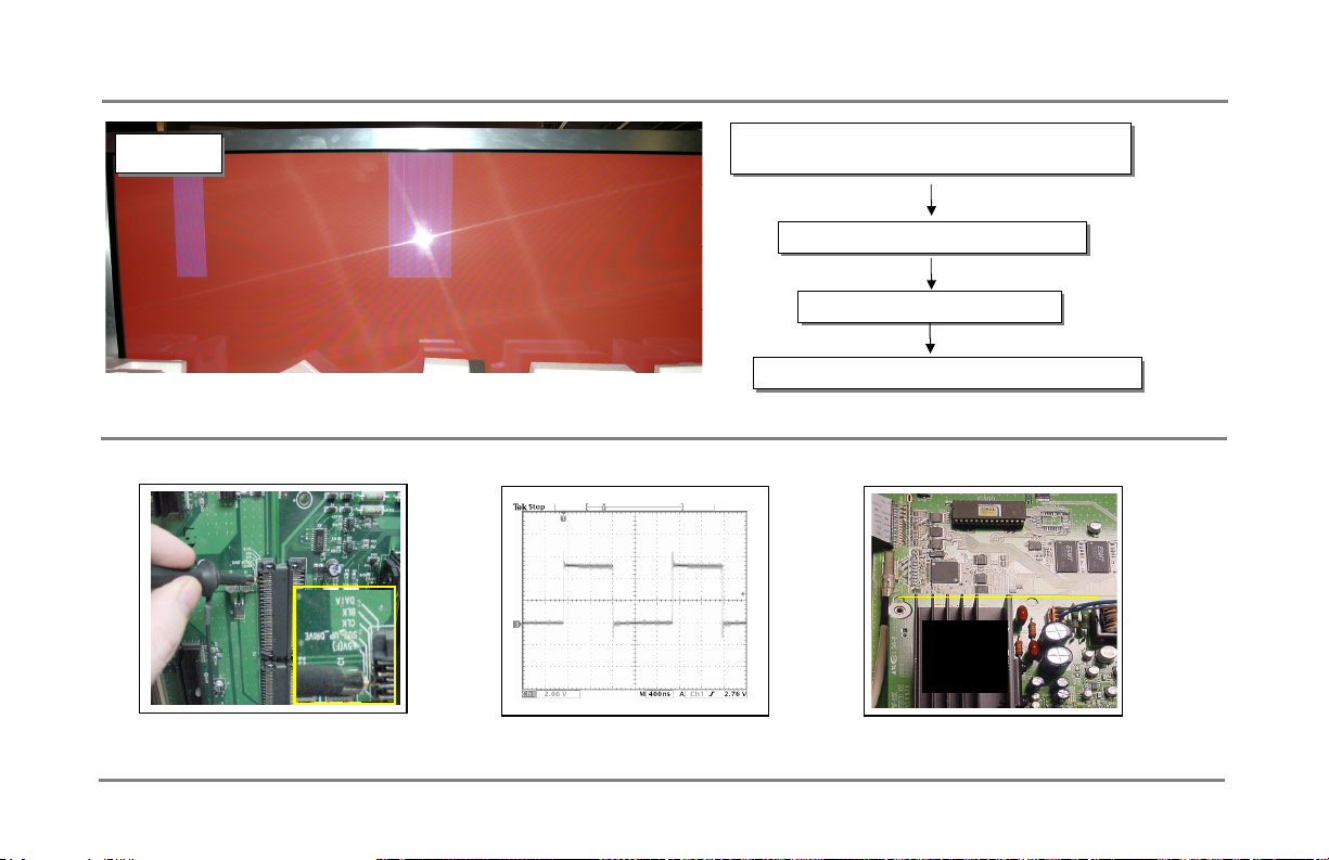
60’’ Known Visual problems with boards that fixed
Fig # 23
Fig # 23
Digital Control Board
Visual Problems
Check & Adjust: PFC / VS / VA voltages to panel
Check & Adjust: PFC / VS / VA voltages to panel
specifications
specifications
Check Y-Sustain Sub-amp wave form
Check Y-Sustain Sub-amp wave form
Okay? Replace Y-Sustain Amp
Okay? Replace Y-Sustain Amp
Not Resolved? Replace Digital Control board
Not Resolved? Replace Digital Control board
Digital
Digital
Control
Control
v.s.c
Board
Y Sustain WF test point
Y Sustain WF
Digital Control board
41
Page 42
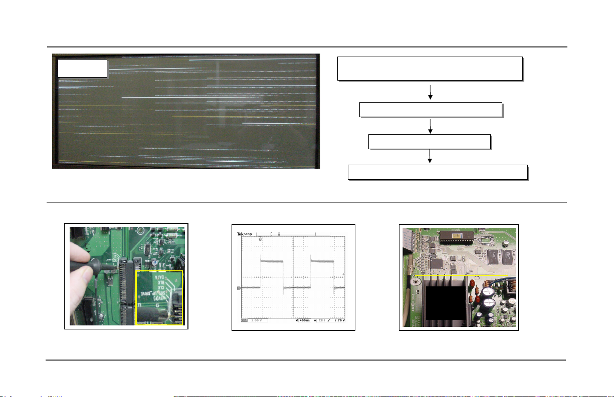
60’’ Known Visual problems with boards that fixed
Fig # 24
Fig # 24
Y-Driver Bottom
Visual Problems
Check & Adjust: PFC / VS / VA voltages to panel
Check & Adjust: PFC / VS / VA voltages to panel
specifications
specifications
Check Y-Sustain Sub-amp wave form
Check Y-Sustain Sub-amp wave form
Okay? Replace Y-Sustain Amp
Okay? Replace Y-Sustain Amp
Not Resolved? Replace Digital Control board
Not Resolved? Replace Digital Control board
Digital
Digital
Control
Control
v.s.c
Board
Y Sustain WF test point
Y Sustain WF
Digital Control board
42
Page 43
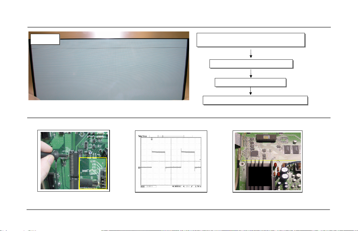
42’’ Known Visual problems with boards that fixed
Fig # 25
Fig # 25
Y-Driver - Top
Visual Problems
Check & Adjust: PFC / VS / VA voltages to panel
Check & Adjust: PFC / VS / VA voltages to panel
specifications
specifications
Check Y-Sustain Sub-amp wave form
Check Y-Sustain Sub-amp wave form
Okay? Replace Y-Sustain Amp
Okay? Replace Y-Sustain Amp
Not Resolved? Replace Digital Control board
Not Resolved? Replace Digital Control board
Digital
Digital
Control
Control
v.s.c
Board
Y Sustain WF test point
Y Sustain WF
Digital Control board
43
Page 44
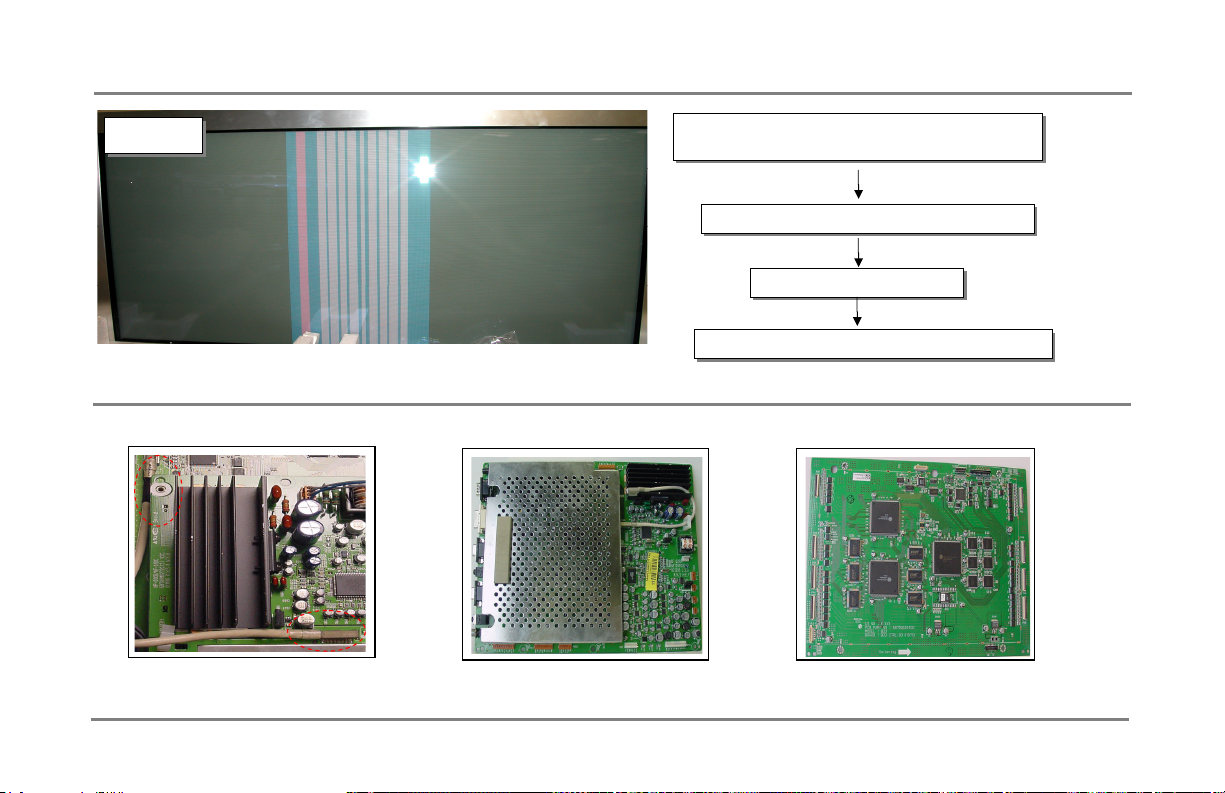
42’’ Known Visual problems with boards that fixed
Fig # 26
Fig # 26
VSC- Board
Visual Problems
Check & Adjust: PFC / VS / VA voltages to panel
Check & Adjust: PFC / VS / VA voltages to panel
specifications
specifications
Check Connection VSC and Digital board
Check Connection VSC and Digital board
Okay? Replace VSC board
Okay? Replace VSC board
Not Resolved? Replace Digital board
Not Resolved? Replace Digital board
VSC to Digital cable
VSC Board
Digital Control
44
Page 45
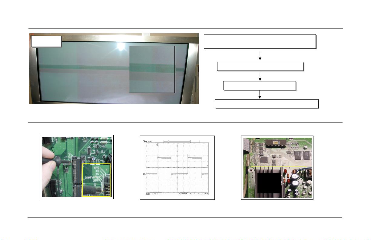
42’’ Known Visual problems with boards that fixed
Fig # 27
Fig # 27
Y-Driver - Top
Visual Problems
Check & Adjust: PFC / VS / VA voltages to panel
Check & Adjust: PFC / VS / VA voltages to panel
specifications
specifications
Check Y-Sustain Sub-amp wave form
Check Y-Sustain Sub-amp wave form
Okay? Replace Y-Sustain Amp
Okay? Replace Y-Sustain Amp
Not Resolved? Replace Digital Control board
Not Resolved? Replace Digital Control board
Digital
Digital
Control
Control
v.s.c
Board
Y Sustain WF test point
Y Sustain WF
Digital Control board
45
Page 46
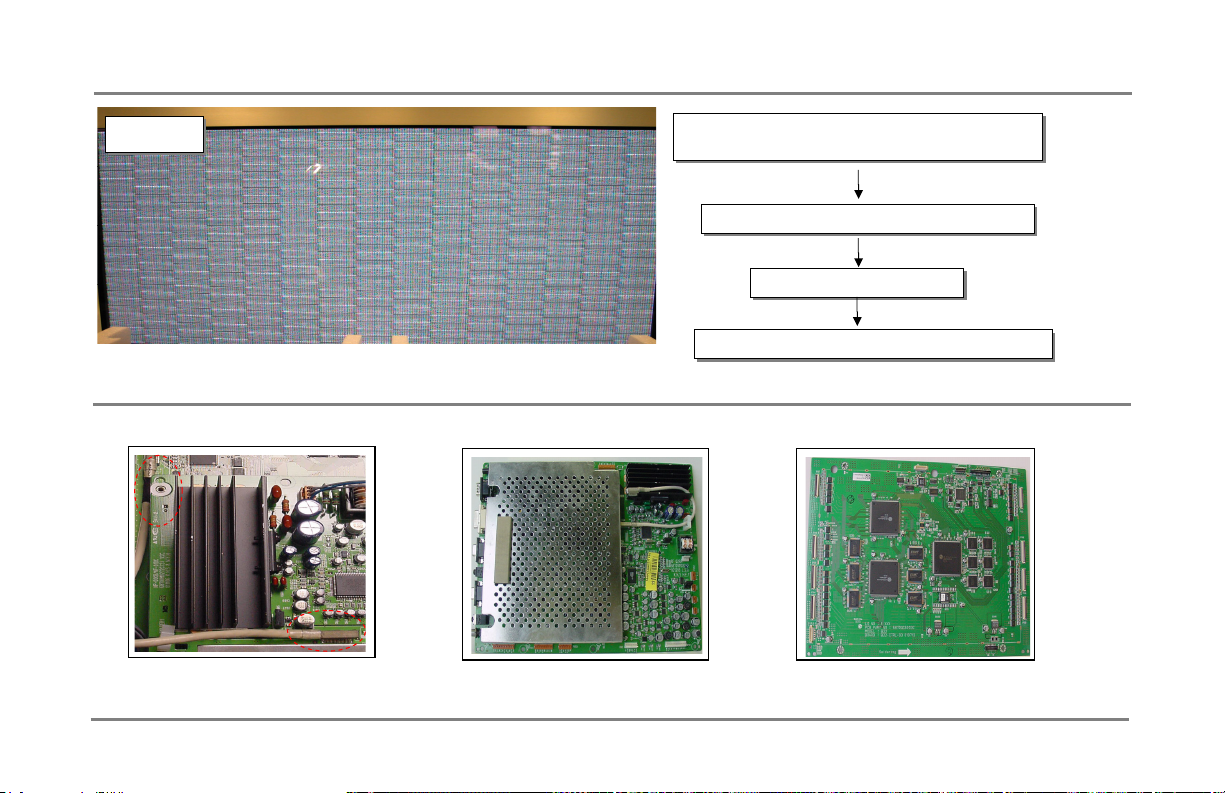
42’’ Known Visual problems with boards that fixed
Fig # 28
Fig # 28
VSC- Board
Visual Problems
Check & Adjust: PFC / VS / VA voltages to panel
Check & Adjust: PFC / VS / VA voltages to panel
specifications
specifications
Check Connection VSC and Digital board
Check Connection VSC and Digital board
Okay? Replace VSC board
Okay? Replace VSC board
Not Resolved? Replace Digital board
Not Resolved? Replace Digital board
VSC to Digital cable
46
Page 47
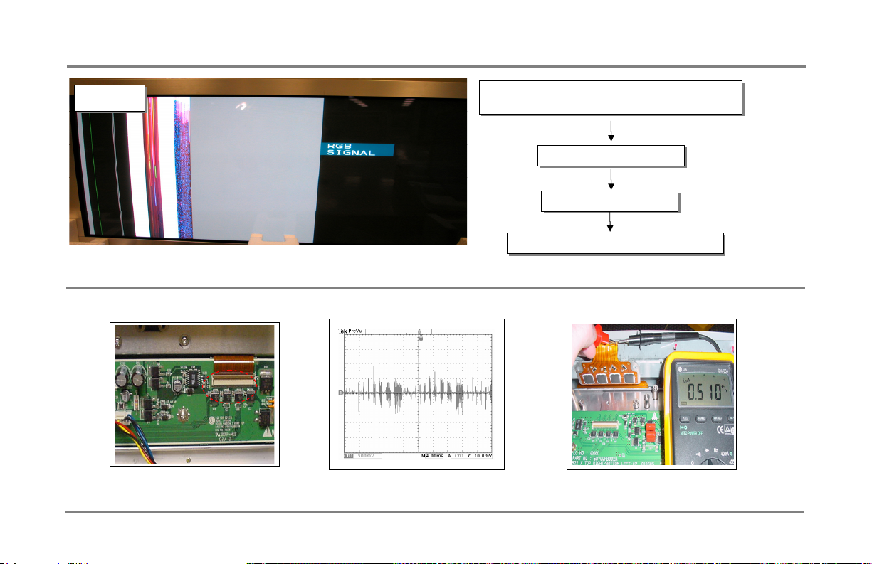
42’’ Known Visual problems with boards that fixed
Fig # 29
Fig # 29
X- Board ( Top Right)
Visual Problems
Check & Adjust: PFC / VS / VA voltages to panel
Check & Adjust: PFC / VS / VA voltages to panel
specifications
specifications
Check X-board wave form
Check X-board wave form
Okay? Replace X-Board
Okay? Replace X-Board
Not Resolved? Check for C.O.F IC Short
Not Resolved? Check for C.O.F IC Short
X-Board WF test point
ER down X- board
47
C.O.F IC test 4 Defective Panel
Page 48
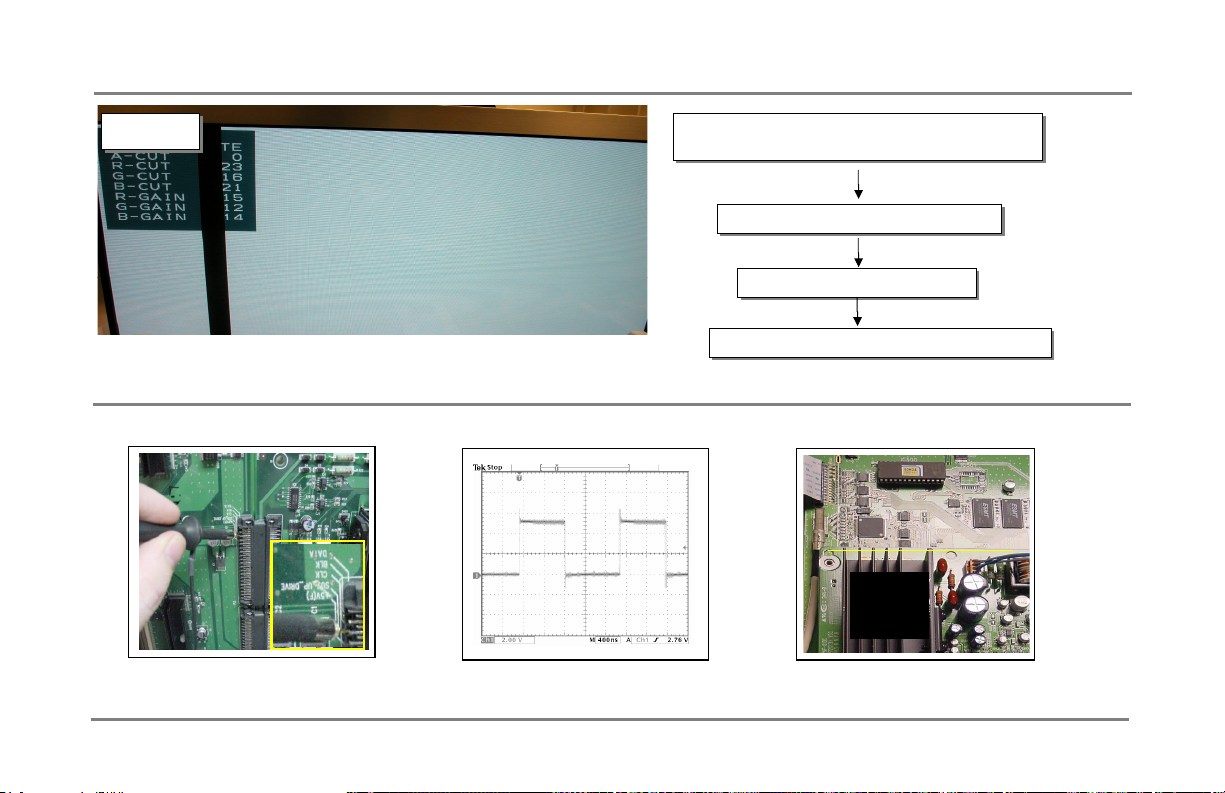
42’’ Known Visual problems with boards that fixed
Fig # 30
Fig # 30
X-Drive Board
Visual Problems
Check & Adjust: PFC / VS / VA voltages to panel
Check & Adjust: PFC / VS / VA voltages to panel
specifications
specifications
Check Y-Sustain Sub-amp wave form
Check Y-Sustain Sub-amp wave form
Okay? Replace Y-Sustain Amp
Okay? Replace Y-Sustain Amp
Not Resolved? Replace Digital Control board
Not Resolved? Replace Digital Control board
Digital
Digital
Control
Control
v.s.c
Board
Y Sustain WF test point
Y Sustain WF
Digital Control board
48
Page 49
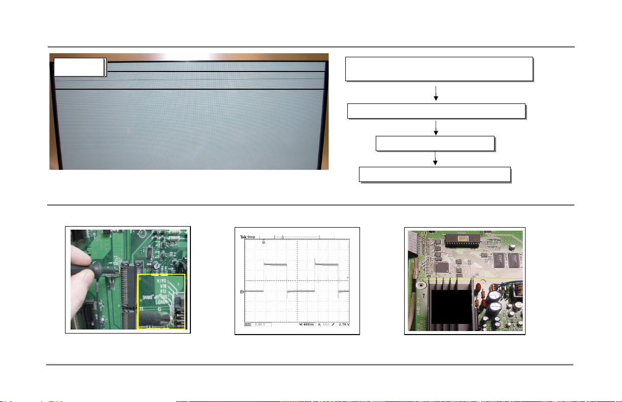
50’’ Known Visual problems with boards that fixed
Fig # 31
Fig # 13
Fig # 31
Fig # 13
Y-Driver Amp upper
Visual Problems
Check & Adjust: PFC / VS / VA voltages to panel
Check & Adjust: PFC / VS / VA voltages to panel
specifications
specifications
Not okay, Check Y-Sustain Sub-amp wave form
Not okay, Check Y-Sustain Sub-amp wave form
Okay, Replace Y-Sustain Amp
Okay, Replace Y-Sustain Amp
Not okay. Replace Digital Control board
Not okay. Replace Digital Control board
Digital
Digital
Control
Control
v.s.c
Board
Y Sustain WF test point
Y Sustain WF
Digital Control board
49
Page 50
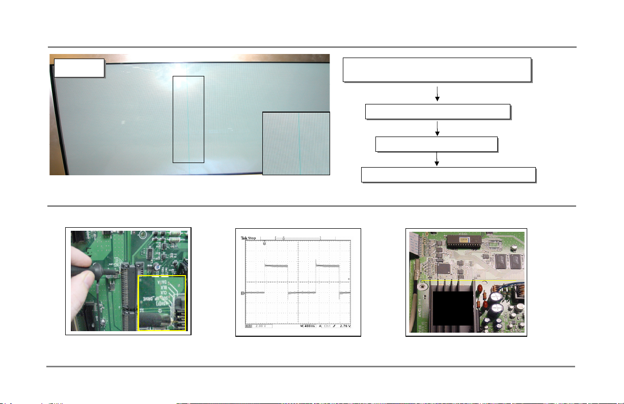
50’’ Known Visual problems with boards that fixed
Fig # 32
Fig # 32
Digital Control board
Visual Problems
Check & Adjust: PFC / VS / VA voltages to panel
Check & Adjust: PFC / VS / VA voltages to panel
specifications
specifications
Check Y-Sustain Sub-amp wave form
Check Y-Sustain Sub-amp wave form
Okay? Replace Y-Sustain Amp
Okay? Replace Y-Sustain Amp
Not Resolved? Replace Digital Control board
Not Resolved? Replace Digital Control board
Digital
Digital
Control
Control
v.s.c
Board
Y Sustain WF test point
Y Sustain WF
Digital Control board
50
Page 51
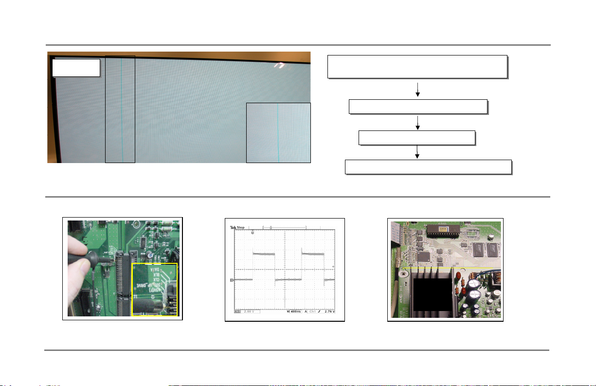
50’’ Known Visual problems with boards that fixed
Fig # 33
Fig # 33
Digital Control Board
Visual Problems
Check & Adjust: PFC / VS / VA voltages to panel
Check & Adjust: PFC / VS / VA voltages to panel
specifications
specifications
Check Y-Sustain Sub-amp wave form
Check Y-Sustain Sub-amp wave form
Okay? Replace Y-Sustain Amp
Okay? Replace Y-Sustain Amp
Not Resolved? Replace Digital Control board
Not Resolved? Replace Digital Control board
Digital
Digital
Control
Control
v.s.c
Board
Y Sustain WF test point
Y Sustain WF
Digital Control board
51
Page 52
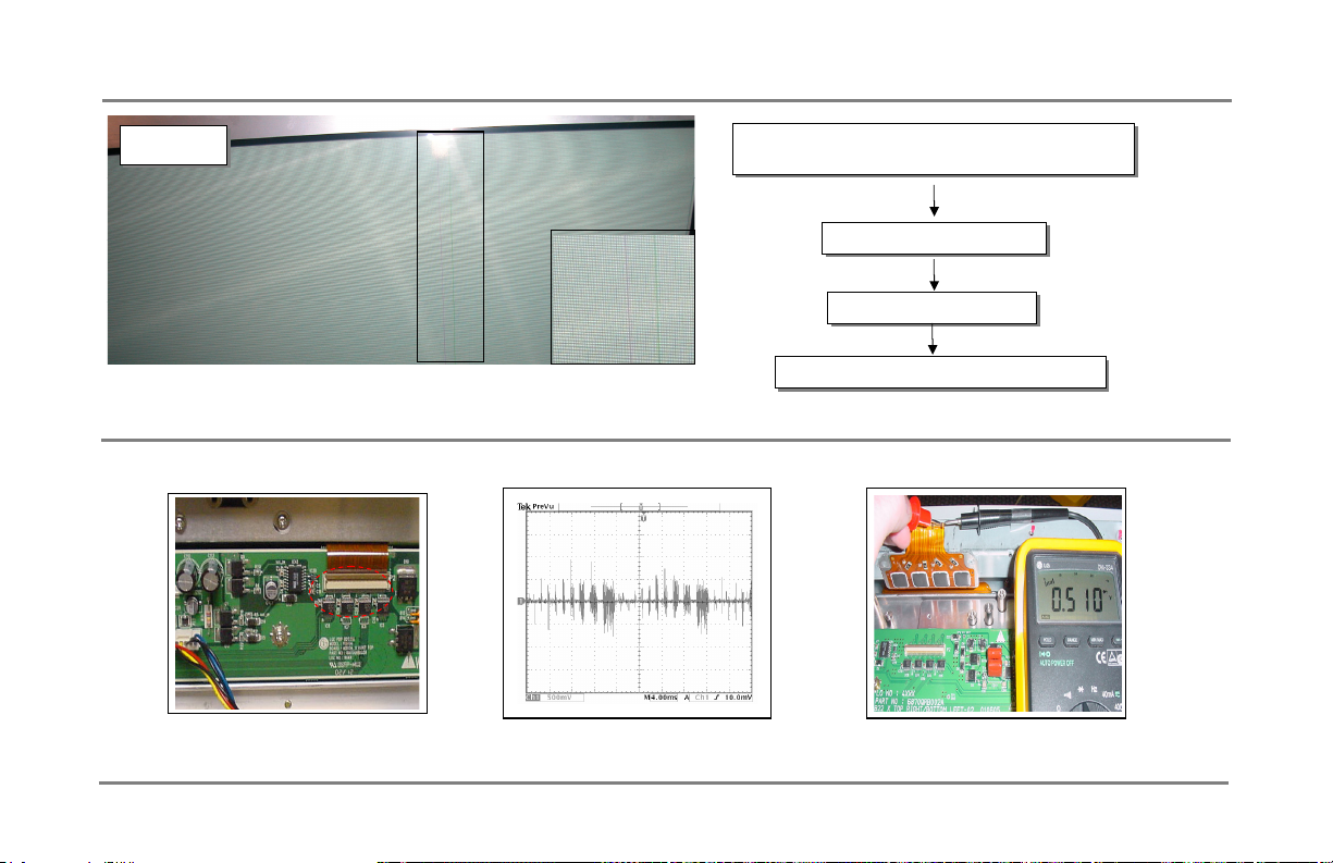
50’’ Known Visual problems with boards that fixed
Fig # 34
Fig # 34
VSC Board
Visual Problems
Check & Adjust: PFC / VS / VA voltages to panel
Check & Adjust: PFC / VS / VA voltages to panel
specifications
specifications
Check X-board wave form
Check X-board wave form
Okay? Replace X-Board
Okay? Replace X-Board
Not Resolved? Check for C.O.F IC Short
Not Resolved? Check for C.O.F IC Short
X-Board WF test point
ER down X- board
52
C.O.F IC test 4 Defective Panel
Page 53
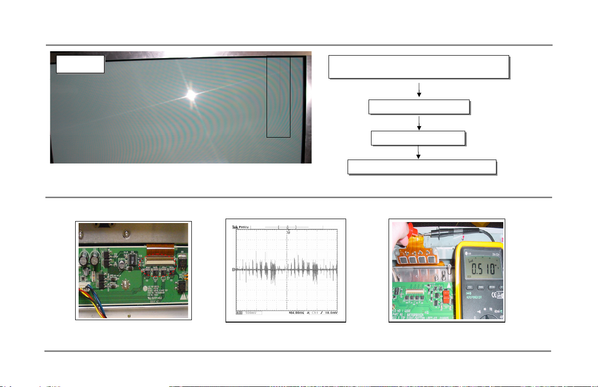
50’’ Known Visual problems with boards that fixed
Fig # 36
Fig # 36
X-Board upper right
Visual Problems
Check & Adjust: PFC / VS / VA voltages to panel
Check & Adjust: PFC / VS / VA voltages to panel
specifications
specifications
Check X-board wave form
Check X-board wave form
Okay? Replace X-Board
Okay? Replace X-Board
Not Resolved? Check for C.O.F IC Short
Not Resolved? Check for C.O.F IC Short
X-Board WF test point
ER down X- board
53
C.O.F IC test 4 Defective Panel
Page 54
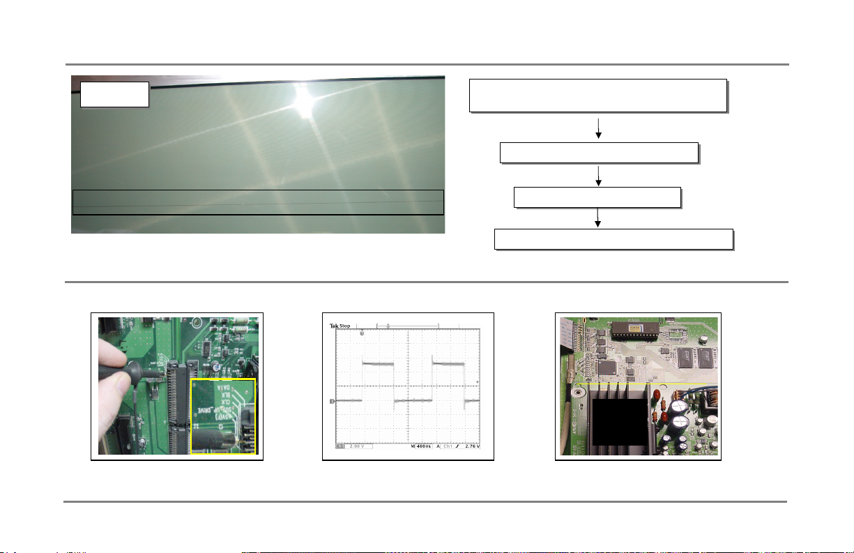
50’’ Known Visual problems with boards that fixed
Fig # 35
Fig # 35
Y- Driver Amp bottom
Visual Problems
Check & Adjust: PFC / VS / VA voltages to panel
Check & Adjust: PFC / VS / VA voltages to panel
specifications
specifications
Check Y-Sustain Sub-amp wave form
Check Y-Sustain Sub-amp wave form
Okay? Replace Y-Sustain Amp
Okay? Replace Y-Sustain Amp
Not Resolved? Replace Digital Control board
Not Resolved? Replace Digital Control board
Digital
Digital
Control
Control
v.s.c
Board
Y Sustain WF test point
Y Sustain WF
Digital Control board
54
Page 55
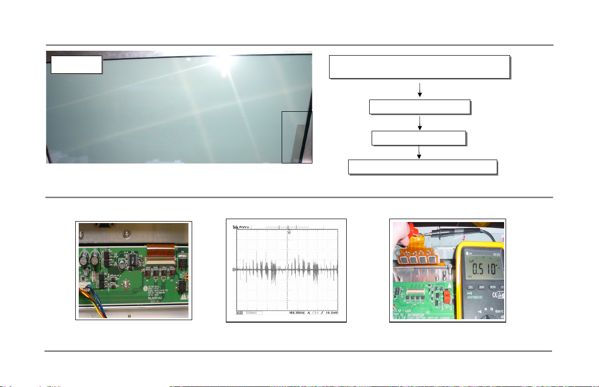
50’’ Known Visual problems with boards that fixed
Fig # 37
Fig # 37
X- Board ( Bottom Left)
Visual Problems
Check & Adjust: PFC / VS / VA voltages to panel
Check & Adjust: PFC / VS / VA voltages to panel
specifications
specifications
Check X-board wave form
Check X-board wave form
Okay? Replace X-Board
Okay? Replace X-Board
Not Resolved? Check for C.O.F IC Short
Not Resolved? Check for C.O.F IC Short
X-Board WF test point
ER down X- board
55
C.O.F IC test 4 Defective Panel
Page 56
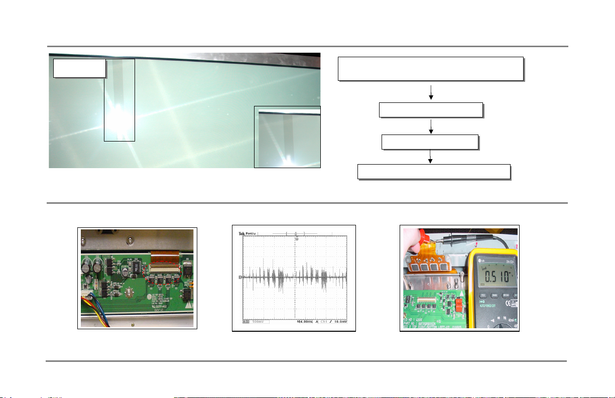
50’’ Known Visual problems with boards that fixed
Fig # 38
Fig # 38
X- Board ( Upper Right)
Visual Problems
Check & Adjust: PFC / VS / VA voltages to panel
Check & Adjust: PFC / VS / VA voltages to panel
specifications
specifications
Check X-board wave form
Check X-board wave form
Okay? Replace X-Board
Okay? Replace X-Board
Not Resolved? Check for C.O.F IC Short
Not Resolved? Check for C.O.F IC Short
X-Board WF test point
ER down X- board
56
C.O.F IC test 4 Defective Panel
Page 57
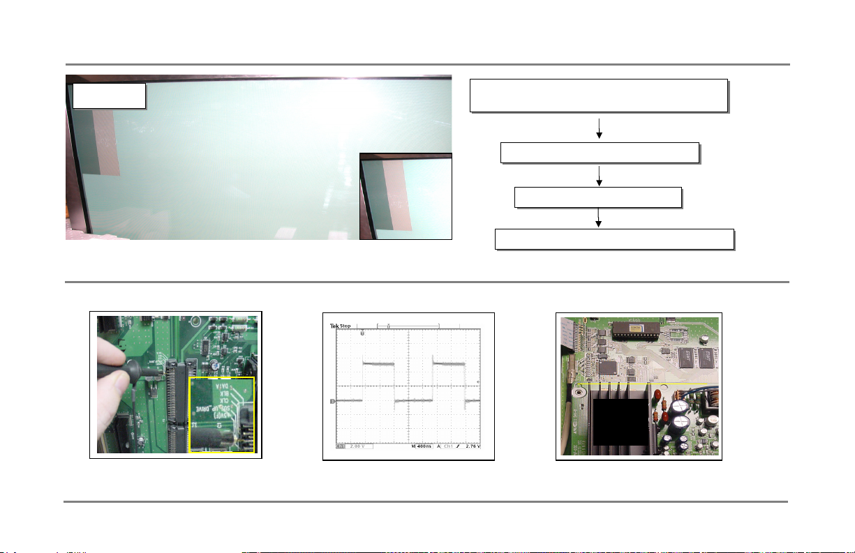
50’’ Known Visual problems with boards that fixed
Fig # 39
Fig # 39
Digital Control Board
Visual Problems
Check & Adjust: PFC / VS / VA voltages to panel
Check & Adjust: PFC / VS / VA voltages to panel
specifications
specifications
Check Y-Sustain Sub-amp wave form
Check Y-Sustain Sub-amp wave form
Okay? Replace Y-Sustain Amp
Okay? Replace Y-Sustain Amp
Not Resolved? Replace Digital Control board
Not Resolved? Replace Digital Control board
Digital
Digital
Control
Control
v.s.c
Board
Y Sustain WF test point
Y Sustain WF
Digital Control board
57
Page 58
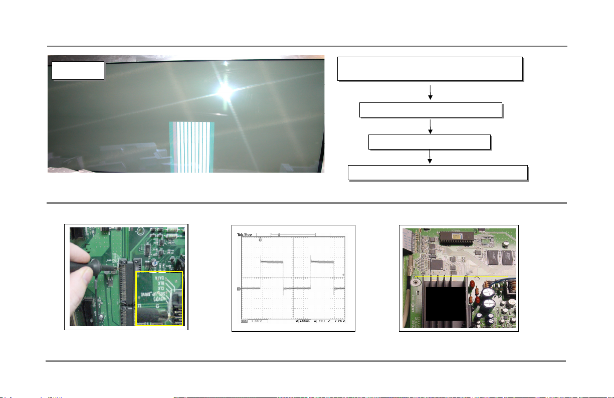
50’’ Known Visual problems with boards that fixed
Fig # 40
Fig # 40
Y- Driver Bottom
Visual Problems
Check & Adjust: PFC / VS / VA voltages to panel
Check & Adjust: PFC / VS / VA voltages to panel
specifications
specifications
Check Y-Sustain Sub-amp wave form
Check Y-Sustain Sub-amp wave form
Okay? Replace Y-Sustain Amp
Okay? Replace Y-Sustain Amp
Not Resolved? Replace Digital Control board
Not Resolved? Replace Digital Control board
Digital
Digital
Control
Control
v.s.c
Board
Y Sustain WF test point
Y Sustain WF
Digital Control board
58
Page 59
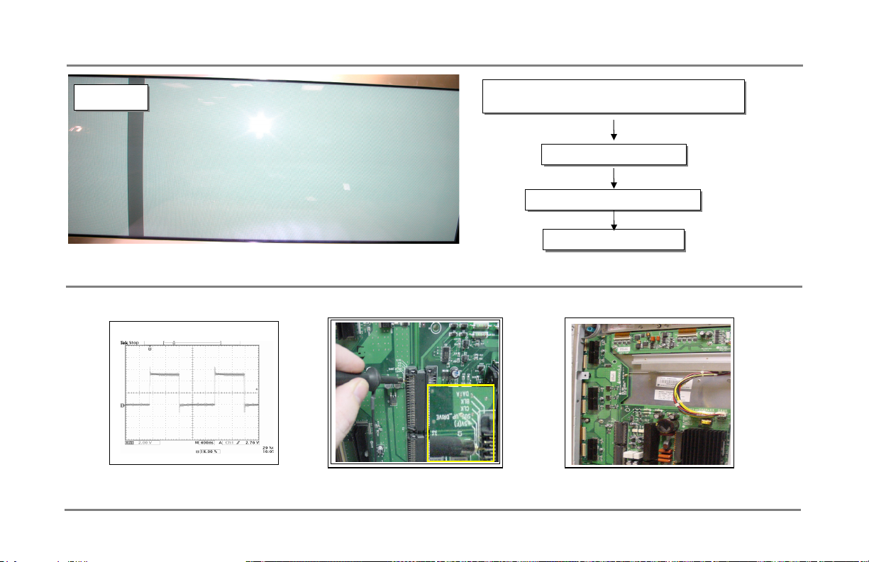
50’’ Known Visual problems with boards that fixed
Fig # 41
Fig # 41
X-Drive Top
Visual Problems
Check & Adjust: PFC / VS / VA voltages to panel
Check & Adjust: PFC / VS / VA voltages to panel
specifications 61
specifications 61
Check X-Board waveform
Check X-Board waveform
Okay? Check for C.O.F IC Short
Okay? Check for C.O.F IC Short
Shorted? Defective Panel
Shorted? Defective Panel
Y Sustain WF
Y Sustain WF test point
59
Y Sustain Sub-Amp board
Page 60
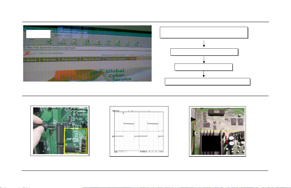
50’’ Known Visual problems with boards that fixed
Fig # 42
Fig # 42
Digital Control Board
Visual Problems
Check & Adjust: PFC / VS / VA voltages to panel
Check & Adjust: PFC / VS / VA voltages to panel
specifications
specifications
Check Y-Sustain Sub-amp wave form
Check Y-Sustain Sub-amp wave form
Okay? Replace Y-Sustain Amp
Okay? Replace Y-Sustain Amp
Not Resolved? Replace Digital Control board
Not Resolved? Replace Digital Control board
Digital
Digital
Control
Control
v.s.c
Board
Y Sustain WF test point
Y Sustain WF
Digital Control board
60
Page 61
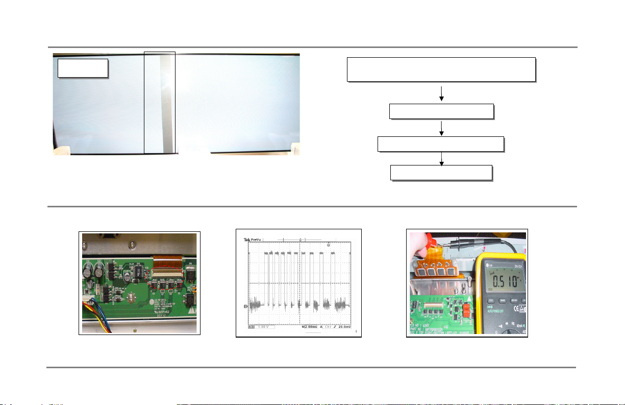
Known Visual problems & found panel defective
Fig # 43
Fig # 43
Visual Problems
Check & Adjust: PFC / VS / VA voltages to panel
Check & Adjust: PFC / VS / VA voltages to panel
specifications
specifications
Check X-Board waveform
Check X-Board waveform
Okay? Check for C.O.F IC Short
Okay? Check for C.O.F IC Short
C.O.F IC – Ribbon shorted/ Part of Panel
Defective Panel
X-Board WF test point
X-Board Sustain WF
61
Shorted? Defective Panel
Shorted? Defective Panel
C.O.F IC test 4 Defective Panel
Page 62
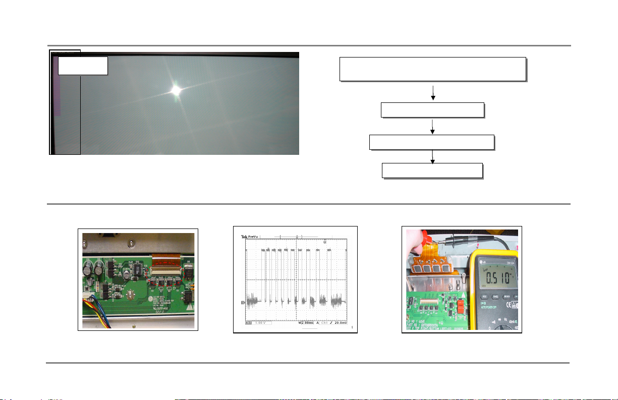
Known Visual problems & found panel defective
Fig # 45
Fig # 45
Visual Problems
Check & Adjust: PFC / VS / VA voltages to panel
Check & Adjust: PFC / VS / VA voltages to panel
specifications
specifications
Check X-Board waveform
Check X-Board waveform
Okay? Check for C.O.F IC Short
Okay? Check for C.O.F IC Short
Data @ X-Board – Yes/ tested for shorted
C.O.F IC – Ribbon shorted/ Defective Panel
X-Board WF test point
X-Board Sustain WF
63
Shorted? Defective Panel
Shorted? Defective Panel
C.O.F IC test 4 Defective Panel
Page 63
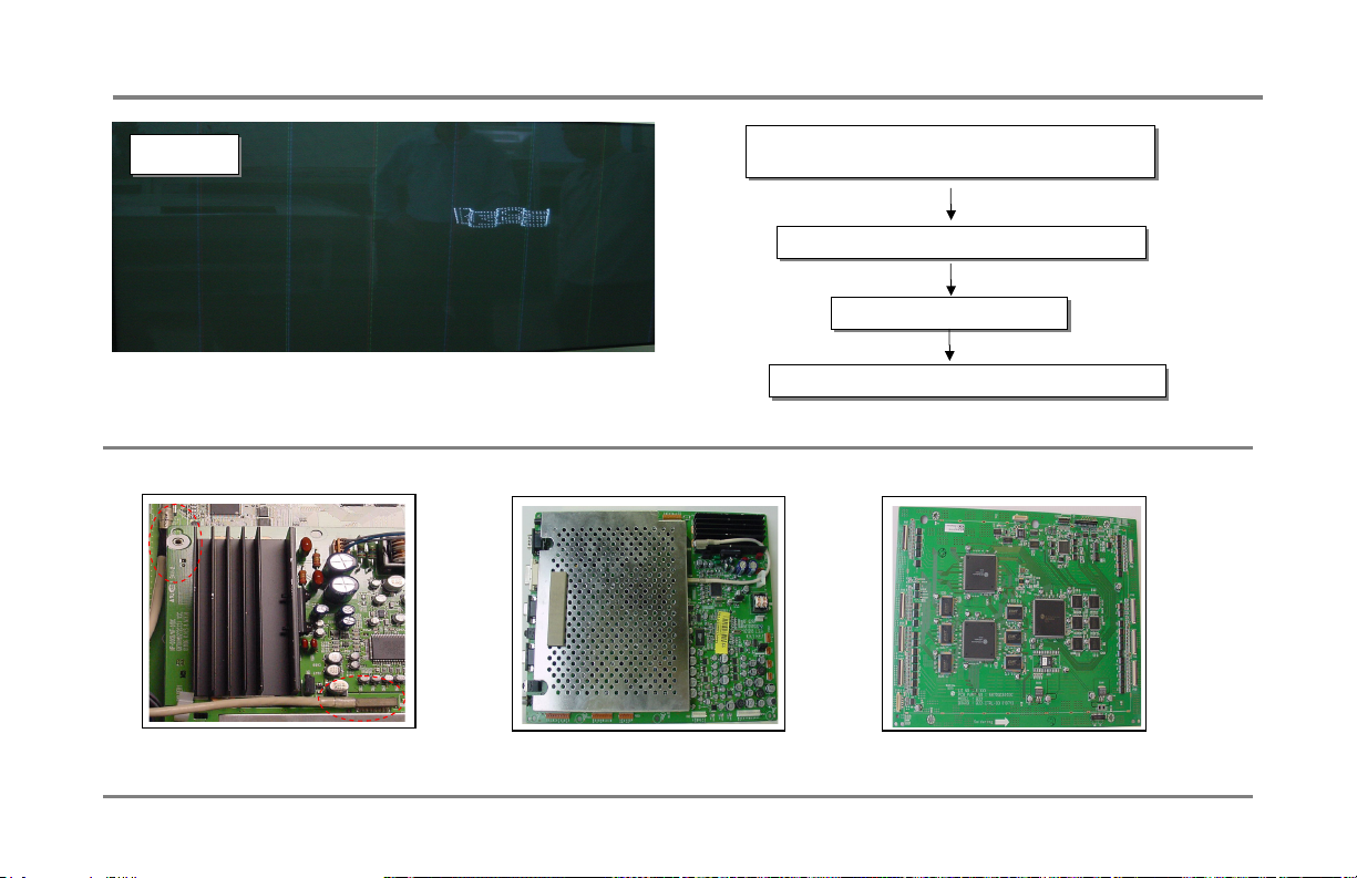
Known Visual problems & found panel defective
Fig # 46
Fig # 46
Display’s waves – V.S.C Board defective
Visual Problems
Check & Adjust: PFC / VS / VA voltages to panel
Check & Adjust: PFC / VS / VA voltages to panel
specifications
specifications
Check Connection VSC and Digital board
Check Connection VSC and Digital board
Okay? Replace VSC board
Okay? Replace VSC board
Not Resolved? Replace Digital board
Not Resolved? Replace Digital board
VSC to Digital cable
VSC Board
Digital Control
64
Page 64
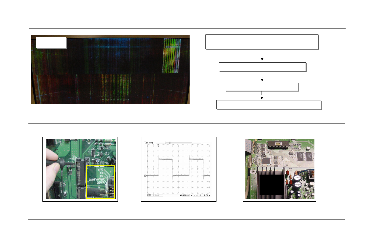
50’’ Known Visual problems with boards that fixed
Fig # 47
Fig # 47
Display’s Vertical Bars – Defective Y-Sub-amp
Visual Problems
Check & Adjust: PFC / VS / VA voltages to panel
Check & Adjust: PFC / VS / VA voltages to panel
specifications
specifications
Check Y-Sustain Sub-amp wave form
Check Y-Sustain Sub-amp wave form
Okay? Replace Y-Sustain Amp
Okay? Replace Y-Sustain Amp
Not Resolved? Replace Digital Control board
Not Resolved? Replace Digital Control board
Digital
Digital
Control
Control
v.s.c
Board
Y Sustain WF test point
Y Sustain WF
Digital Control board
65
Page 65
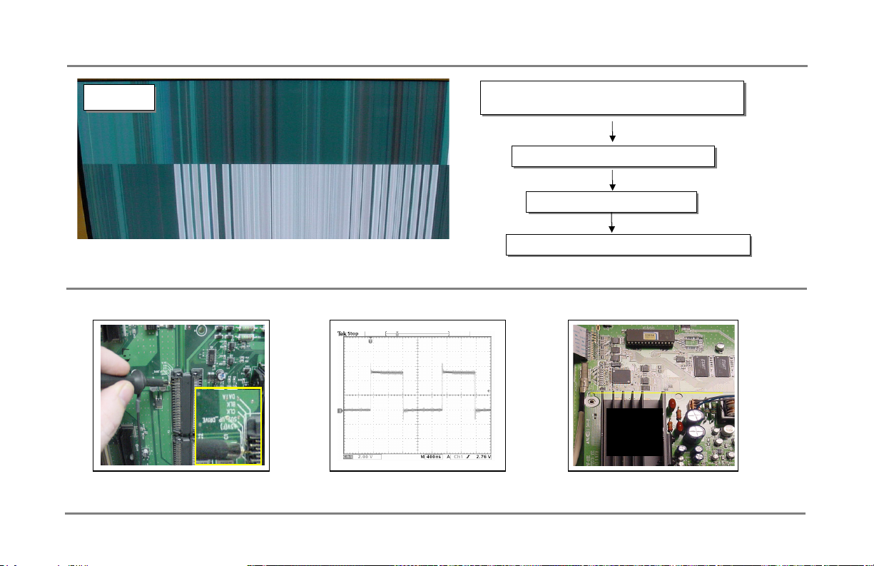
50’’ Known Visual problems with boards that fixed
Fig # 48
Fig # 48
Display’s Vertical Bars – Defective Y-Sub-amp
Visual Problems
Check & Adjust: PFC / VS / VA voltages to panel
Check & Adjust: PFC / VS / VA voltages to panel
specifications
specifications
Check Y-Sustain Sub-amp wave form
Check Y-Sustain Sub-amp wave form
Okay? Replace Y-Sustain Amp
Okay? Replace Y-Sustain Amp
Not Resolved? Replace Digital Control board
Not Resolved? Replace Digital Control board
Digital
Digital
Control
Control
v.s.c
Board
Y Sustain WF test point
Y Sustain WF
Digital Control board
66
Page 66
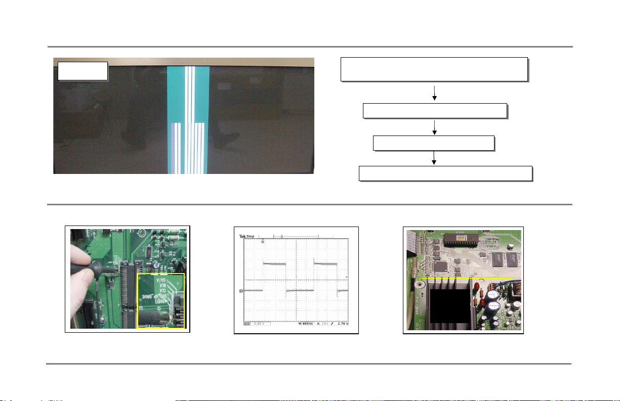
50’’ Known Visual problems with boards that fixed
Fig # 49
Fig # 49
Y-Driver - Top
Visual Problems
Check & Adjust: PFC / VS / VA voltages to panel
Check & Adjust: PFC / VS / VA voltages to panel
specifications
specifications
Check Y-Sustain Sub-amp wave form
Check Y-Sustain Sub-amp wave form
Okay? Replace Y-Sustain Amp
Okay? Replace Y-Sustain Amp
Not Resolved? Replace Digital Control board
Not Resolved? Replace Digital Control board
Digital
Digital
Control
Control
v.s.c
Board
Y Sustain WF test point
Y Sustain WF
Digital Control board
67
Page 67
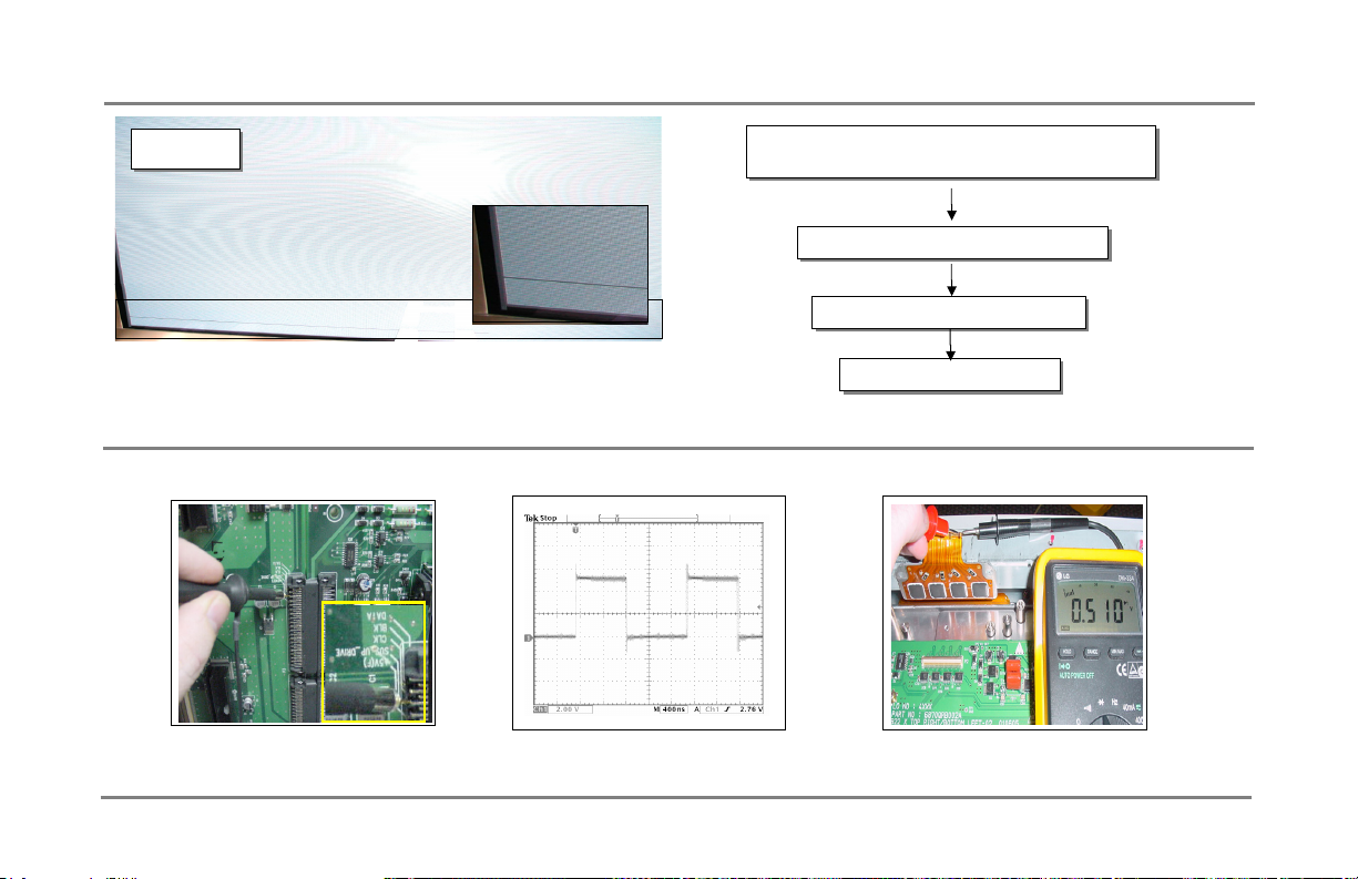
Known Visual problems & found panel defective
Fig # 44
Fig # 44
Visual Problems
Check & Adjust: PFC / VS / VA voltages to panel
Check & Adjust: PFC / VS / VA voltages to panel
specifications
specifications
Check Y-Sustain Sub-amp wave form
Check Y-Sustain Sub-amp wave form
Okay? Check for C.O.F IC Short
Okay? Check for C.O.F IC Short
C.O.F IC – Ribbon shorted/ Part of Panel
Defective Panel
Y-Sustain Sub-amp test point
Y Sustain WF
62
Shorted? Defective Panel
Shorted? Defective Panel
C.O.F IC test 4 Defective Panel
Page 68
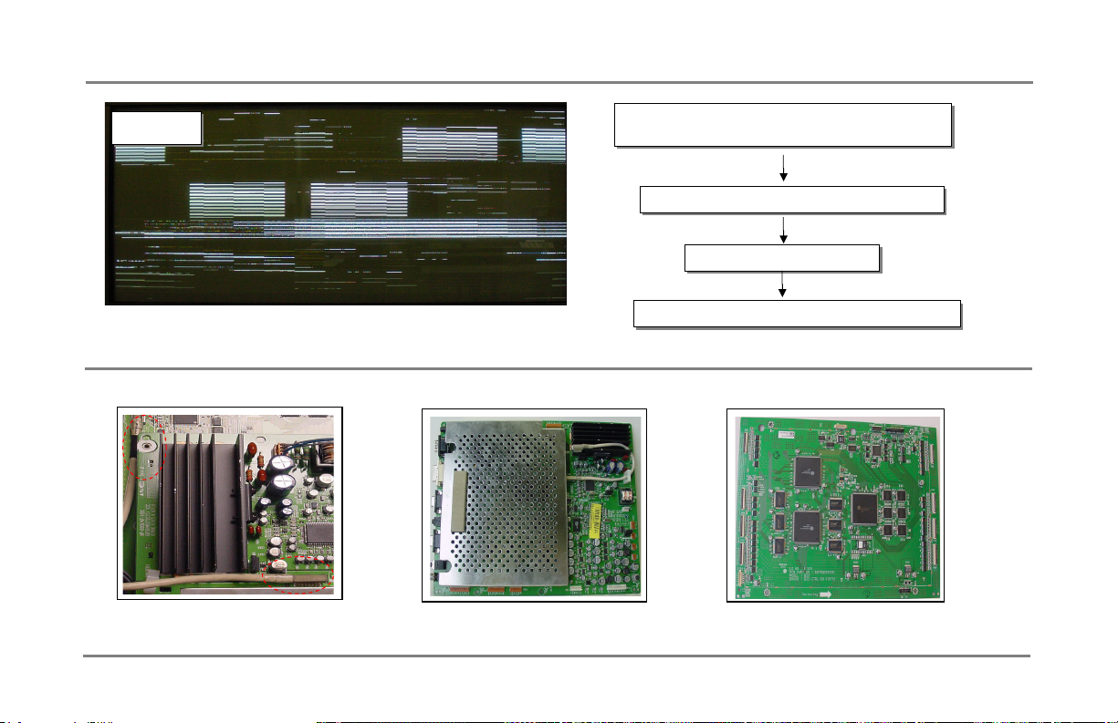
Known Visual problems & found panel defective
Fig # 50
Fig # 50
VSC- Board
Visual Problems
Check & Adjust: PFC / VS / VA voltages to panel
Check & Adjust: PFC / VS / VA voltages to panel
specifications
specifications
Check Connection VSC and Digital board
Check Connection VSC and Digital board
Okay? Replace VSC board
Okay? Replace VSC board
Not Resolved? Replace Digital board
Not Resolved? Replace Digital board
VSC to Digital cable
VSC Board
Digital Control
68
Page 69
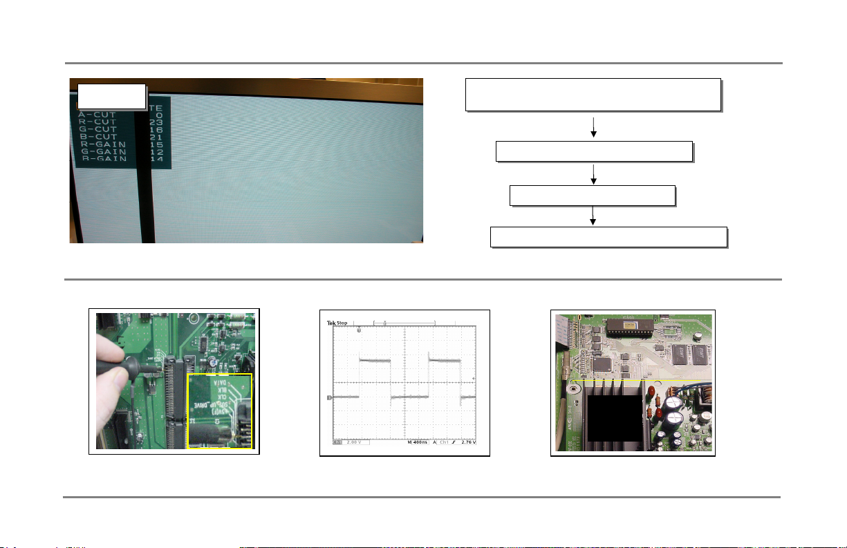
Known Visual problems & found panel defective
Fig # 51
Fig # 51
Y-Driver - Top
Visual Problems
Check & Adjust: PFC / VS / VA voltages to panel
Check & Adjust: PFC / VS / VA voltages to panel
specifications
specifications
Check Y-Sustain Sub-amp wave form
Check Y-Sustain Sub-amp wave form
Okay? Replace Y-Sustain Amp
Okay? Replace Y-Sustain Amp
Not Resolved? Replace Digital Control board
Not Resolved? Replace Digital Control board
Digital
Digital
Control
Control
v.s.c
Board
Y Sustain WF test point
Y Sustain WF
Digital Control board
69
Page 70
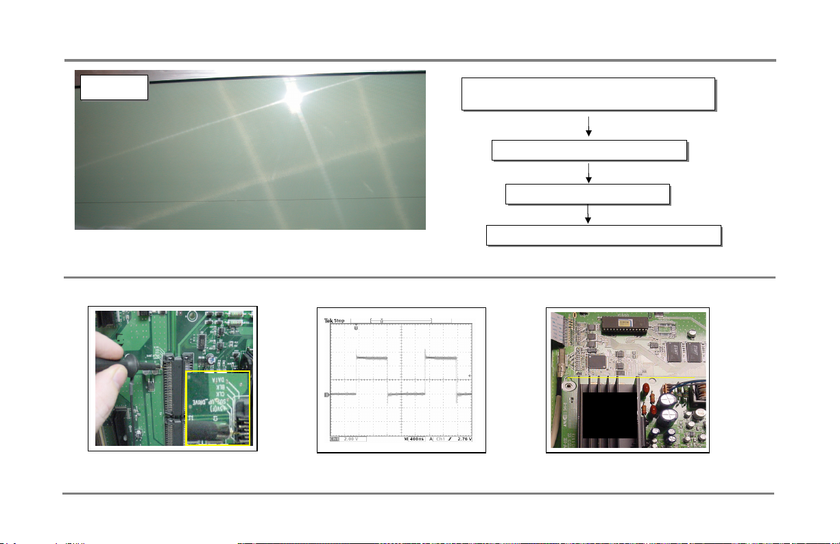
Known Visual problems & found panel defective
Visual Problems
Fig # 52
Fig # 52
Y-Driver Amp upper
Y Sustain WF test point
Y Sustain WF
Check & Adjust: PFC / VS / VA voltages to panel
Check & Adjust: PFC / VS / VA voltages to panel
specifications
specifications
Check Y-Sustain Sub-amp wave form
Check Y-Sustain Sub-amp wave form
Okay? Replace Y-Sustain Amp
Okay? Replace Y-Sustain Amp
Not Resolved? Replace Digital Control board
Not Resolved? Replace Digital Control board
Digital
Digital
Control
Control
v.s.c
Board
Digital Control board
70
Page 71
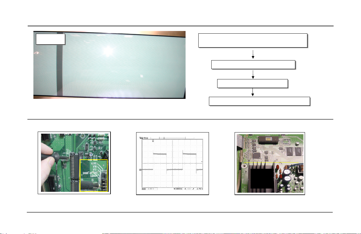
Known Visual problems & found panel defective
Fig # 53
Fig # 53
Digital Control board
Visual Problems
Check & Adjust: PFC / VS / VA voltages to panel
Check & Adjust: PFC / VS / VA voltages to panel
specifications
specifications
Check Y-Sustain Sub-amp wave form
Check Y-Sustain Sub-amp wave form
Okay? Replace Y-Sustain Amp
Okay? Replace Y-Sustain Amp
Not Resolved? Replace Digital Control board
Not Resolved? Replace Digital Control board
Digital
Digital
Control
Control
v.s.c
Board
Y Sustain WF test point
Y Sustain WF
Digital Control board
71
Page 72
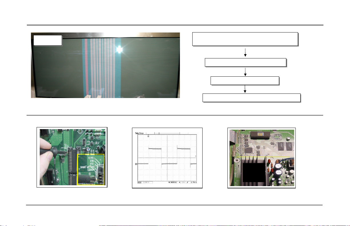
Known Visual problems & found panel defective
Fig # 54
Fig # 54
Digital Control Board
Visual Problems
Check & Adjust: PFC / VS / VA voltages to panel
Check & Adjust: PFC / VS / VA voltages to panel
specifications
specifications
Check Y-Sustain Sub-amp wave form
Check Y-Sustain Sub-amp wave form
Okay? Replace Y-Sustain Amp
Okay? Replace Y-Sustain Amp
Not Resolved? Replace Digital Control board
Not Resolved? Replace Digital Control board
Digital
Digital
Control
Control
v.s.c
Board
Y Sustain WF test point
Y Sustain WF
Digital Control board
72
Page 73
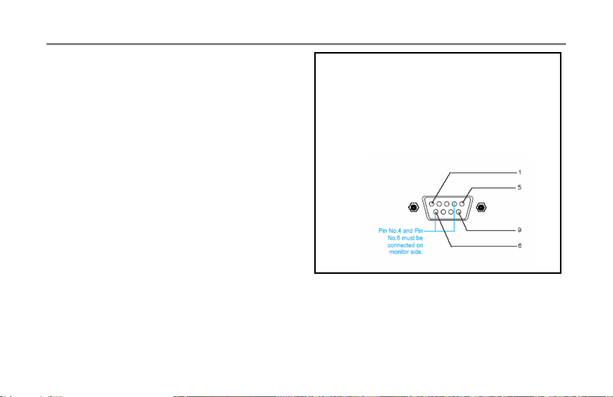
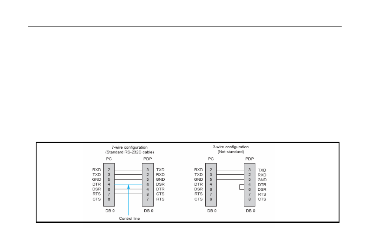
RS-232 (Activating remote link) for controlling Panel
Installation & Set-up
Type of connector : D-Sub 9-pin male
* Use a null modem cable.
Wire the 7-Wire cable so that each pair of data lines
cross between the two devices. These data line pairs
are RXD (Receive data) and TXD (Transmit data), DTR
(DTE side ready) and DSR (DCE side ready), and RTS
(Ready to send) and CTS (Clear to send).
When using the 3-Wire cable connected to RXD, TXD
and GND; Pin No. 4 (DTR) and Pin No. 6 (DSR) must
be connected to the monitor. (The cable must be
disconnected from the Monitor to be able to use the
remote control and Monitor front panel controls.)
* With the RS-232 input connected, the Monitor cannot
be controlled by both an external control device and the
remote control at the same time. The Monitor can only
be controlled by either the remote control or the external
control device.
Hyper terminal
No. Pin Out/ key
1 No connection
2 RXD (Receive data)
3 TXD (Transmit data)
4 DTR (DTE side ready)
5 GND
6 DSR (DCE side ready)
7 RTS (Ready to send)
8 CTS (Clear to send)
9 No Connection
73
Page 74
RS-232 (Activating remote link) for controlling Panel
Installation & Set-up
7-Wire Cable Configuration
• The Monitor is available to switch between external adjustment
and remote control adjustment using a control line.
Note: If the control line is high, the monitor is controlled by the
external control device. If the control line is low, the Monitor is
controlled by the Monitor's remote control.
3-Wire Cable Configuration
• When using a 3-Wire cable configuration, there is no control
line. The external equipment can command the Monitor to
"change into remote control adjustment mode”. When using a
3-Wire cable configuration, there is no control line. The external
control device must put the Monitor into the "change into remote
control adjustment mode“. The Monitor will then be able to be
controlled by the remote control. If the Monitor is turned back
on, it will revert back to external device control.
• The external control device must put the Monitor into the
"change into remote control adjustment mode "function in 7Wire Configuration.
3-Wire Cable Configuration
• When using a 3-Wire cable configuration, there is no
control line. The external equipment can command the
Monitor to "change into remote control adjustment mode”.
(When using a 3-Wire cable configuration there is no control
line. The external control device must put the Monitor into
the "change into remote control adjustment mode“ & The
Monitor will then be able to be controlled by the remote
control). If the Monitor is turned back on, it will revert back to
external device control.
• The external control device must put the Monitor into the
"change into remote control adjustment mode"function in 7Wire Configuration.
74
Page 75
Definition of cell defect
y
Panel Testing
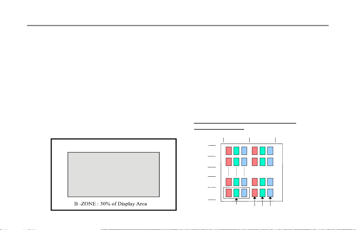
1) Cell defect definition
- Non-ignition dot (dark defect): In a ignited cell, the cell
that an extinguished size is less than 50%. Cells which are
not working.
- Non-extinguishing dot(brightness defect): In an
extinguished cell, the cell that a ignited size is more than
50%. Cell which is always working “ON”.
- Unstable Dot (Flickering): Cell which repeats on
(brightness) and off (darkness).
- Uncontrollable Dot : Cell which is brighter or stays on
longer than other cells around it because of unstable
working condition.
A -ZONE : 70%
of Displa
Area
2) Test results are satisfied with each full red, green, blue,
black and white test pattern.
- Specifically, The full white test pattern is used to decide the
number of continuous cell defects, The full black test pattern is
used to decide the number of Non-extinguishing cell defects.
- The decision distance is 2.2m (3H, 60”) away from the panel,
intensity of illumination is between 100 Lux and 200 Lux.
3) Cell defects do not increase or progress as time goes on.
PDP CELL DISPLAY AND DEFECT ZONES:
Display Dot Diagram
1st Pixel
row
2nd Pixel
row
Pixel
row
Pixel
row
1st Pixel
column
R G B R G B
R G B R G B
R G B R G B
R G B R G B
2nd Pixel
column
Pixel
Sub-Pixel or Cell
75
Page 76
RS-232 program codes
Panel Testing
P
P
5
5
0
0
W
W
P
P
2
2
4
4
6
6
2
2
,
D
D
P
P
P
P
D
D
4
4
P
P
0
0
4
4
V
V
0
0
2
2
VFUNCTION
VFUNCTION
2
2
,
W
W
P
P
P
P
2
2
5
5
4
4
2
2
0
0
0
0
,
,
W
W
V
V
B
B
2
2
2
2
/
/
6
6
4
4
H
H
B
B
P
P
6
6
0
0
W
W
2
2
6
6
,
,
P
P
D
D
P
P
P
5
5
0
0
W
W
2
2
8
8
A
A
XXS-VIDEO
XXS-VIDEO
XXCOMPONENT
XXCOMPONENT
P
P
P
6
6
6
6
D
D
0
0
0
0
P
P
W
W
W
W
6
6
2
2
2
2
0
0
6
6
6
6
W
W
A
A
P
P
S
S
T
T
A
A
R
R
TTYPE
TTYPE
7D6D5D4D3D2D1DFUNCTION
7D6D5D4D3D2D1DFUNCTION
H
H
ST
ST
E
E
A
A
X
X
R
R
C
C
T
T
O
O
BI
BI
D
D
T
T
E
E
0ED501110D5-BIT, DOUBLE-STARTXXXPOWER ON
0ED501110D5-BIT, DOUBLE-STARTXXXPOWER ON
08D500010D5-BIT, DOUBLE-STARTXXXSYSTEM OFF
08D500010D5-BIT, DOUBLE-STARTXXXSYSTEM OFF
C404XXXXXXXPOWER ON
C404XXXXXXXPOWER ON
C504XXPOWER OFF
C504XXPOWER OF F
C504XXXXSYSTEM OFF
C504XXXXSYSTEM O FF
9804XXRGB & POWER ON
9804XXRGB & POWER ON
9804XXRGB-1
9804XXRGB-1
C604XXRGB 2
C604XXRGB 2
5A04XXVIDEO & POWER ON
5A04XXVIDEO & POWER ON
5A04XXVIDEO
5A04XXVIDEO
5104XXS-VIDEO & POWER ON
5104XXS-VIDEO & POWER ON
BF04XXCOMPONENT & POWER ON
BF04XXCOMPONENT & POWER ON
D404FUTURECOMPONENT 2
D404FUTURECOMPONENT 2
7704XXXX16:9 (ASPECT RATIO)
7704XXXX16:9 (ASPECT RATIO)
7604XXXX4:3 (ASPECT RATIO)
7604XXXX4:3 (ASPECT RATIO)
AF04XXXXZOOM (ASPECT RATIO)
AF04XXXXZOOM (ASPECT RATIO)
76
Page 77
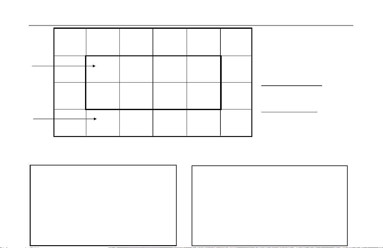
Plasma Cell Defect Form
(01) (02) (03) (04) (05) (06)
A-Zone
Visual Problems
Fax to:
LG Tech Support
Fax #: 256.774.4051
Email: [email protected]
(16) (A) (B) (C) (D) (07)
(15) (E) (F) (G) (H) (08)
B-Zone
(14) (13) (12) (11) (10) (09)
Description:
Non-Extinguishing Pixels
Pixel that remains on/ illuminating
the Sub-pixel Red/ Blue/ Green.
Non-Illuminating Pixels
Pixel that remains off/ not illuminating
the Sub-pixel Red/ Blue/ Green.
Model Number :_____________Serial Number :____________ Servicer Acct :_____________
Customer's Name :______________Date of Purchase:_____________ RA# :
A-Zone (A -H) Cell Defects Location(s) Quantity
Non-Extinguishing Pixels
(Red) _______ ________
(Blue) _______ ________
(Green) _______ ________
Flickering Pixels or Non-Illuminating Pixels
(Red) _______ ________
(Blue) _______ ________
(Green) _______ ________
B-Zone (1 -16) Cell Defects Location(s) Quantity
Non-Extinguishing Pixels
(Red) _______ ________
(Blue) _______ ________
(Green) _______ ________
Flickering Pixels or Non-Illuminating Pixels
(Red) _______ ________
(Blue) _______ ________
77
(Green) _______ ________
___________
Page 78
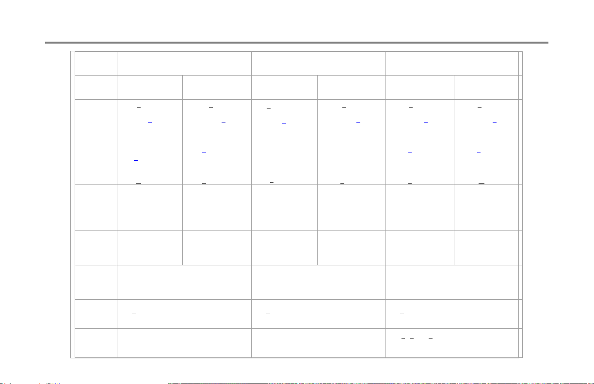
Definition of cell defect
Panel Testing
Div.
Zone A - Zone B - Zone A - Zone B - Zone A – Zone B – Zone
* N<3 [Cells /
RGB screen]
Non
ignition
Dot
And
Unstabl
e Dot
Uncontr
ollable
Dot
Non
extingui
shing
Dot
Defect
distance
Total
Defect
Stain
Total N<
[Cell/ full screen]
*2cell
conjunction
point:
N<
0
*include
Unstable dot:
4
N <
N=0
N=0 N=0 N=0 N=0 N = 0 N = 0
50mm ˺ 50mm ˺
N < 25 [Cell/ full screen] N < 25 [Cell/ full screen] N < 35[Cell/ full screen]
*1˺D˺5, N˺3
*Dപ5, N=0
42ˑ 50ˑ
* N<5 [Cells /
9
RGB screen]
[Cell/ full screen]
conjunction point:
con
N˺2 [Cells/ RGB
screen]
Total N˺6 [Cells
/ full screen]
15
TotalnN<
*2cell
2*3cell
N<
junction point:
N =0
*Unstable dot:
N<
7
•N< [Cells /
RGB screen]
TotalnN< 4
[Cell/full screen]
*2cell
conjunction point:
N<*3cell
conjunction point:
Unstable dot:
N <
N=2
* 1˺D˺5, N˺3
* Dപ5, N=0
N = 0
* N< [Cells /
RGB screen]
[Cell/ full screen]
conjunction point:
conjunction point:
N˺3 [Cells /
RGB screen]
Total N˺ [Cells /
full screen]
11
TotalnN<
*1cell
N<*3cell
N = 0
*Unstable dot:
N<
* N<11 [Cells /
RGB screen]
TotalnN<
[Cell/ full screen]
*2cell
conjunction point:
2*3cell
N<
conjunction point:
N =0
*Unstable dot:
N<
11
N 2 [Cells / RGB
screen]
Total N6 [Cells /
full screen]
D ˻5cm, N 1 (D: Centimeter)
; however, including conjunction cell,
N = 0
* 1<D<5, N < 3 (Stain Distance:˻50 mm)
* D>5, N = 0 (Stain Distance:˻50mm)
60ˑ
* N<12 [Cells /
33
RGB screen]
TotalnN<
[Cell/ full screen]
*2cell
conjunction point:
2*3cell
N<
conjunction point:
N =0
*Unstable dot:
N <
N 3 [Cells / RGB
screen]
Total N9 [Cells /
full screen]
36
12
78
Page 79
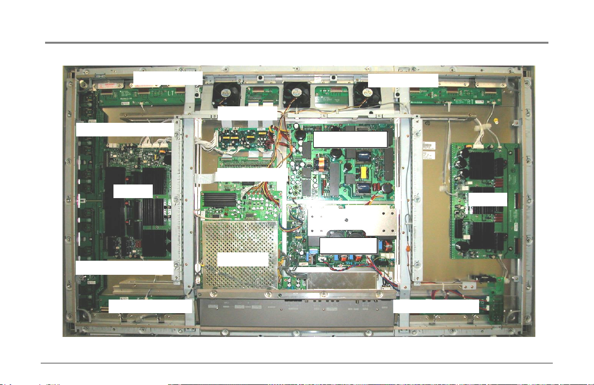
60’’ PZ90V
Configuration diagram
X-Board (L-TOP)
Y-Driver Board (Bottom)
Y-Board
Y-Driver Board (Bottom)
X-Board ( L-Bottom) X-Board ( R- Bottom)
DC/DC Board
Controller Board
VSC Board
X-Board (R-TOP)
POWER Board
POWER Board
PFC Board
PFC Board
Z-Board
Great Company Great People
79
Page 80
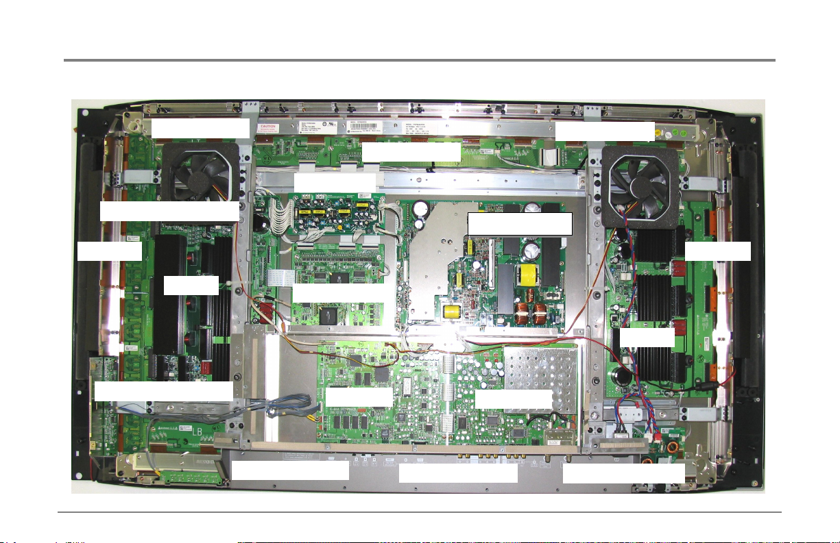
50’’ PV10
Configuration diagram
X-Board (L-TOP)
Y-Driver Board (Bottom)
Y-Board
Y-Driver Board (Bottom)
X-Board ( L-Bottom)
Great Company Great People
X-Board (C-TOP)
DC/DC Board
Controller Board
VSC Board
POWER Board
POWER Board
X-Board ( C-Bottom)
80
X-Board (R-TOP)
Speaker RSpeaker L
Z-Board
Tuner Board
X-Board ( R- Bottom)
Page 81
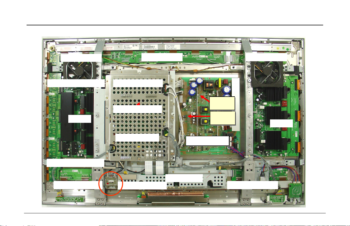
50’’ PZ60,70
Configuration diagram
X-Board (L-TOP)
Y-Driver Board (Bottom) DC/DC Board Down
Y-Board
Y-Driver Board (Bottom)
X-Board ( L-Bottom) X-Board ( R- Bottom)
Great Company Great People
X-Board (C-TOP)
Controller Board UP
VSC Board Down
X-Board ( L-Bottom)
POWER Board
A/V Box-Board
81
Rv401
Rv401
Rv401
Rv401
Vs
Vs
Vs
Vs
Rv601
Rv601
Rv601
Rv601
Va
Va
Va
Va
POWER Board
X-Board (R-TOP)
Z-Board
Page 82
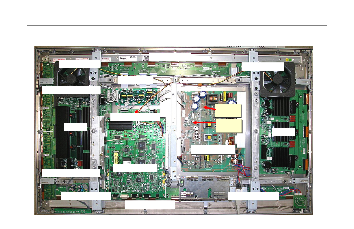
50’’ PZ90V
X-Board (L-TOP)
Y-Driver Board (Bottom)
Y-Board
DC/DC Board
Controller Board UP
X-Board (C-TOP)
Rv401
Rv401
Rv401
Rv401
Vs
Vs
Vs
Vs
Rv601
Rv601
Rv601
Rv601
Va
Va
Va
Va
POWER Board
POWER Board
Configuration diagram
X-Board (R-TOP)
Z-Board
Y-Driver Board (Bottom)
X-Board ( L-Bottom) X-Board ( R- Bottom)
Great Company Great People
VSC Board Down
X-Board ( C-Bottom)
82
Page 83
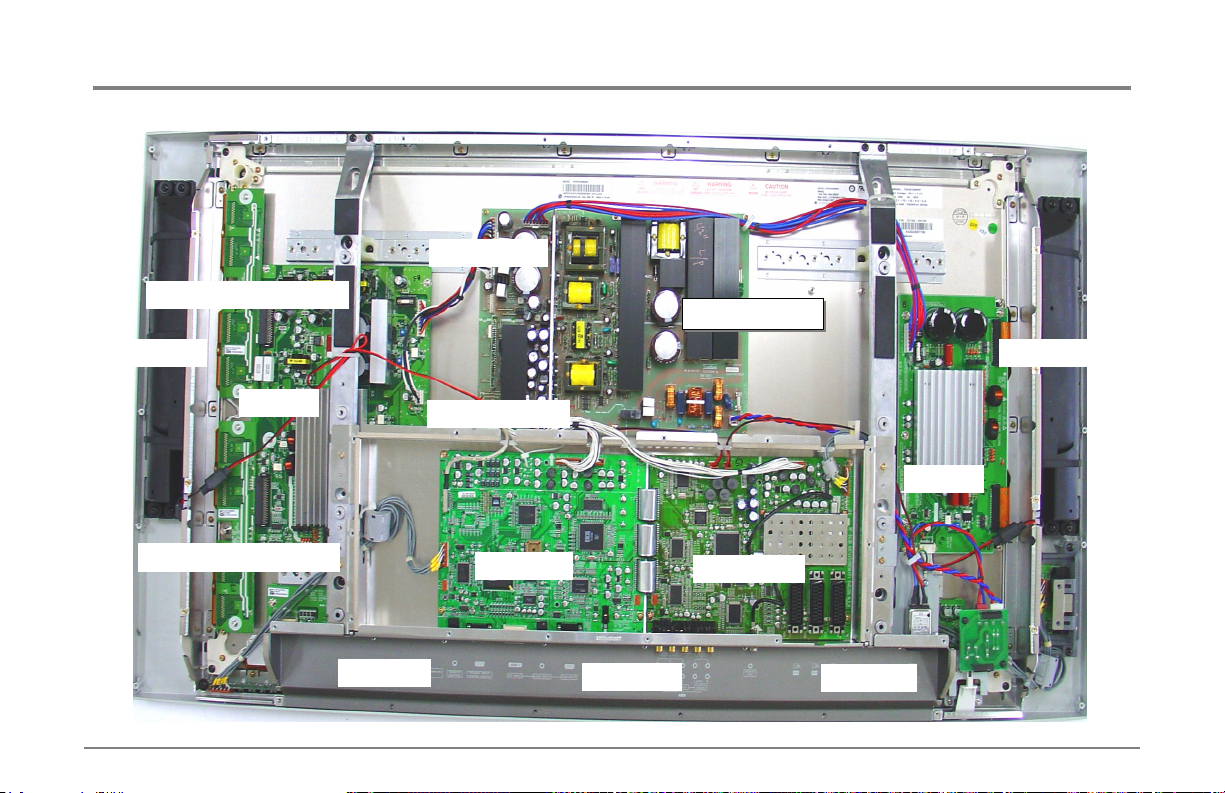
42’’ PZ10
Configuration diagram
DC/DC Board
Y-Driver Board (Bottom)
Y-Board
Y-Driver Board (Bottom)
X-Board L
Great Company Great People
Controller Board
VSC Board
X-Board C
83
POWER Board
POWER Board
Tuner Board
Speaker RSpeaker L
Z-Board
X-Board R
Page 84
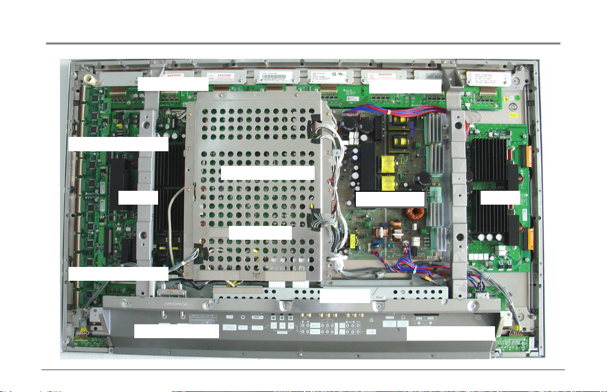
42’’ PZ60,70
Configuration diagram
X-Board (L-TOP)
Y-Driver Board (Bottom)
Y-Driver Board (Bottom)
X-Board ( L-Bottom)
Controller Board Down
VSC Board UP
A/V Board
X-Board (R-TOP)
POWER Board
POWER Board
Z-BoardY-Board
X-Board ( R- Bottom)
Great Company Great People
84
Page 85
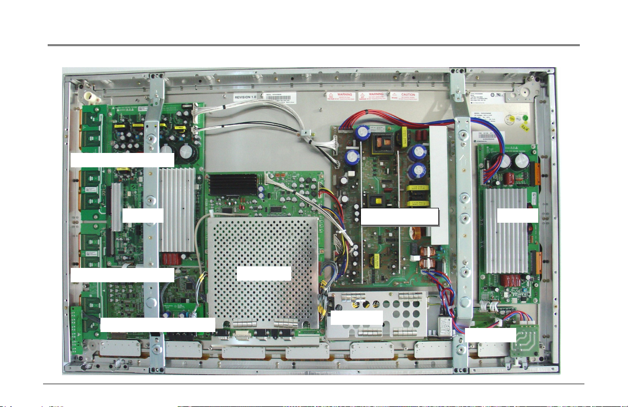
42’’ PZ90V
Y-Driver Board (Bottom)
Configuration diagram
Y-Driver Board (Bottom)
Control Board + X-Board L
Great Company Great People
VSC Board
85
POWER Board
POWER Board
A/V Board
Z-BoardY-Board
X-Board R
Page 86

 Loading...