

Page 1

PLASMA MONITOR
SERVICE MANUAL
CAUTION
BEFORE SERVICING THE CHASSIS,
READ THE SAFETY PRECAUTIONS IN THIS MANUAL.
CHASSIS : RF-02KE
MODEL : MU-50PZ41V MU-50PZ41VB
website:http://biz.LGservice.com
e-mail:http://www.LGEservice.com/techsup.html
Page 2

CONTENTS
SAFETY PRECAUTIONS ...................................................................................3
DISCRIPTION OF CONTROLS ......................................................................... 4
ADJUSTMENT INSTRUCTIONS ........................................................................6
BLOCK DIAGRAM...............................................................................................9
EXPLODED VIEW..............................................................................................10
EXPLODED VIEW PARTS LIST ........................................................................11
REPLACEMENT PARTS LIST...........................................................................12
SCHEMATIC DIAGRAM ........................................................................................
PRINTED CIRCUIT BOARD ..................................................................................
Page 3
SAFETY PRECAUTIONS
Many electrical and mechanical parts in this chassis have special safety-related characteristics. These parts are identified by in
the Schematic Diagram and Replacement Parts List.
It is essential that these special safety parts should be replaced with the same components as recommended in this manual to
prevent X-RADIATION, Shock, Fire, or other Hazards.
Do not modify the original design without permission of manufacturer.
General Guidance
An lsolation Transformer should always be used during
the servicing of a receiver whose chassis is not isolated from
the AC power line. Use a transformer of adequate power rating
as this protects the technician from accidents resulting in
personal injury from electrical shocks.
It will also protect the receiver and it's components from being
damaged by accidental shorts of the circuitary that may be
inadvertently introduced during the service operation.
If any fuse (or Fusible Resistor) in this monitor is blown, replace
it with the specified.
When replacing a high wattage resistor (Oxide Metal Film
Resistor, over 1W), keep the resistor 10mm away from PCB.
Keep wires away from high voltage or high temperature parts.
Due to high vacuum and large surface area of picture tube,
extreme care should be used in handling the Picture Tube.
Do not lift the Picture tube by it's Neck.
Leakage Current Cold Check(Antenna Cold Check)
With the instrument AC plug removed from AC source,
connect an electrical jumper across the two AC plug prongs.
Place the AC switch in the on positioin, connect one lead of
ohm-meter to the AC plug prongs tied together and touch other
ohm-meter lead in turn to each exposed metallic parts such as
antenna terminals, phone jacks, etc.
If the exposed metallic part has a return path to the chassis, the
measured resistance should be between 1MΩ and 5.2MΩ.
When the exposed metal has no return path to the chassis the
reading must be infinite.
An other abnormality exists that must be corrected before the
receiver is returned to the customer.
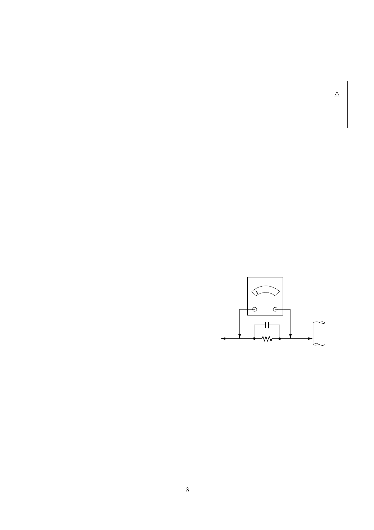
Leakage Current Hot Check (See below Figure)
Plug the AC cord directly into the AC outlet.
Do not use a line Isolation Transformer during this check.
Connect 1.5K/10watt resistor in parallel with a 0.15uF capacitor
between a known good earth ground (Water Pipe, Conduit, etc.)
and the exposed metallic parts.
Measure the AC voltage across the resistor using AC
voltmeter with 1000 ohms/volt or more sensitivity.
Reverse plug the AC cord into the AC outlet and repeat AC
voltage measurements for each esposed metallic part. Any
voltage measured must not exceed 0.75 volt RMS which is
corresponds to 0.5mA.
In case any measurement is out of the limits sepcified, there is
possibility of shock hazard and the set must be checked and
repaired before it is returned to the customer.
Leakage Current Hot Check circuit
1.5 Kohm/10W
To Instrument's
exposed
METALLIC PARTS
Good Earth Ground
such as WATER PIPE,
CONDUIT etc.
AC Volt-meter
IMPORTANT SAFETY NOTICE
0.15uF
Page 4
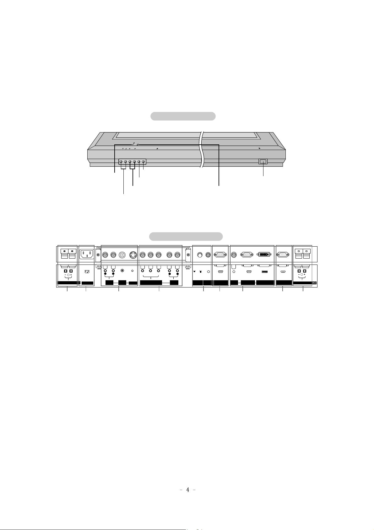
CONTROLS DESCRIPTION
Monitor Controls
Connection Options
VOL. MENU INPUT SELECT
ON/OFF
Main Power Button
INPUT SELECT Button
VOLUME (FF,GG) Buttons
Power Standby Indicator
Illuminates red in standby mode,
Illuminates green when the
Monitor is turned on
Remote Control Sensor
MENU Button
DD,EE
Buttons
Y PBP
R
( )( )
R
(MONO)
R
AUDIO
ON/ OFF
L
R
AUDIO
L
( )( )
L
AC INPUT
(8Ω)
EXTERNAL SPEAKER
COMPONENT
(DVD/DTV INPUT)
RGB1 OUTPUT
(PC/DTV OUTPUT)
LOCK
REMOTE
CONTROL
CONTROL
RGB1 INPUT
(PC/DTV INPUT)
INPUT
AUDIO
INPUT
AUDIO
INPUT
AUDIO
INPUT
VIDEO
RGB2 INPUT
(DIGITAL RGB INPUT)
RS-232C INPUT
(CONTROL/SERVICE)
S-VIDEO
EXTERNAL SPEAKER
1 2 3 4 7 85 6 1
1. EXTERNAL SPEAKER (8 ohm output)
Connect to optional external speaker(s).
* For further information, refer to ‘Speaker & Speaker Stand’
manual.
2. POWER CORD SOCKET
This Monitor operates on an AC power. The voltage is indicated on the Specifications page. Never attempt to operate
the Monitor on DC power.
3. AUDIO/VIDEO INPUT JACKS
Connect audio/video out from external equipment to these
jacks.
S-VIDEO INPUTS (S-VIDEO)
Connect video out from an S-VIDEO VCR to the S-VIDEO
input.
4. COMPONENT(DVD/DTV INPUT)/AUDIO INPUT JACKS
5. CONTROL LOCK Switch
REMOTE CONTROL
When “CONTROLLOCK” is set “ON”, Monitor is operated by
the external control device.
6. RGB1 OUTPUT(PC/DTV OUTPUT) JACKS
You can watch the RGB1 signal on another monitor, connect
RGB1 OUTPUT (PC/DTV OUTPUT) to another monitor’s
PC input port.
7. AUDIO INPUT/RGB1 INPUT(PC/DTV INPUT)/
RGB2 INPUT(DIGITAL RGB INPUT) JACKS
Connect the monitor output socket of the PC to this socket.
8. RS-232C INPUT(CONTROL/SERVICE) PORT
Connect to the RS-232C port on a PC.
Front Panel Controls
Back Connection Panel
Page 5
Remote Control Key Functions
- When using the remote control aim it at the remote control sensor of the Monitor.
- There's maybe a defect in consecutive operation of remote control in specified brightness according to this monitor
feature.
1 2 3
4 5 6
7 8
0
9
POWER
SLEEP INPUT SELECT
APC DASP
ARC PIP ARC
PIP
TWIN PICTURE
SWAP
MENU MUTE
OK
VOL
POWER STOP
PLAY FF
REC
REW
P/STILL
WIN.SIZE
WIN.POSITION
ZOOM +
ZOOM -
SPLIT ZOOM
VOL
SUB INPUT
POWER
Switches the Monitor on from
standby or off to standby.
SLEEP
Sets the sleep timer.
APC
Adjusts the factory preset picture
according to the room.
ARC
Changes the picture format.
PIP
Switches the sub picture on or off.
SWAP
Exchanges main and sub picture
images.
MENU
Displays on screen menus one by one.
Exits the current menu.
Memorizes menu changes.
NUMBER buttons
WIN. SIZE
Adjusts the sub picture size.
WIN.POSITION
Moves the sub picture.
SPLIT ZOOM
Enlarge the screen with regular
ration.
ZOOM-/ZOOM+
Enlarges or reduces
the main picture size.
VCR BUTTONS
Controls a LG video cassette
recorder.
OK
DD / EE
Selects a menu option.
FF / GG
(Volume button)
Increases/decreases sound level.
Adjusts menu settings.
INPUT SELECT
Selects:
VIDEO, S-VIDEO, RGB1/2 or
COMPONENT mode.
DASP
To select the sound appropriate to
your viewing program character:
FLAT,SPORTS, CINEMA,MUSIC, or
USER
PIP ARC
Changes the PIP picture format.
SUB INPUT
Selects the input mode for the sub
picture.
MUTE
Switches the sound on or off.
TWIN PICTURE
Page 6

1. Application Object
These instructions are applied to all of the PDP monitor, RF02CA.
2. Notes
(1) Because this is not a hot chassis, it is not necessary to use
an isolation transformer. However, the use of isolation
transformer will help protect test instrument.
(2) Adjustment must be done in the correct order.
(3) The adjustment must be performed in the circumstance of
25±5°C of temperature and 65±10% of relative humidity if
there is no specific designation.
(4) The input voltage of the receiver must keep 110~240V,
50/60Hz in adjusting.
(5) The receiver must be operated for about 15 minutes prior
to the adjustment.
1) After receiving 100% white pattern(06CH), the receiver
must be operate prior to adjustment. (Or white condition
in HEAT-RUN mode)
2) Enter into HEAT-RUN mode
- Press the POWER ON KEY on R/C for adjustment.
- OSD display HEAT-RUN WHITE and screen display
100% full WHITE PATTERN.
[ Set is activated HEAT-RUN without signal generator in
this mode.
[ Single color pattern of HEAT-RUN mode uses to check
PANEL. (RED/BLUE/GREEN)
[Caution]
If you turn on a still screen more than 20 minutes
(Especially Digital pattern(13 CH), Cross Hatch
Pattern), a afterimage may be occur in the black level
part of the screen.
3. RGB Auto Cut-Off & MIN Bias
Adjustment
(1) Input Full Back (0 Gray) signal which generated from
Pattern Generator into CVBS and RGB1 Input part.
(2) Press POWER ON KEY on R/C for adjustment and select
AUTO-CUT(Cut-off Auto Adjustment)
(3) Press Vol. + key and operate TO SET
(4) Screen adjustment starts with Full Black screen.
Original Window screen will be presented about 5-6
seconds later. And if there is a mark of OK OSD, then the
Auto Cut-off and Min-Bias adjustment will be completed.
(5) Pass to the next MAX Bias Adjustment after Adjustment.
[ Replace PDP Module or Power Board, adjust certainly Power
PCB Assy Voltage.
4. MAX Bias Adjustment
(1) Input Full White (255 Gray) signal which generated from
Pattern Generator into CVBS and RGB1 Input part.
(2) Press POWER ON KEY on R/C for adjustment and select
MAX-BIAS
(3) Press Vol. + key and operate TO SET
(4) Original Full White screen will be presented about 1~2
seconds later. And if there is a mark of OK OSD, then the
Min-Bias adjustment will be completed.
(5) After adjustment, press
key to save adjustment and
come out of the adjustment mode.
O
You can check whether circuit adjustment is operated well or
not, as below.
(1) Display RGB1 to the Main picture, CVBS to the Sub
picture in the TWIN PICTURE.
(2) To check the MIN-Bias, input Full Black (0 gray) signal into
CVBS and RGB1 input part at the same time in the Pattern
Generator.
(3) To check the MAX-Bias, input Full White (255 gray) signal
into CVBS and RGB1 input part at the same time in the
Pattern Generator.
(4) Compare Black Level with White Level by eyes. And if
there is no Level difference, the adjustment is completed
well.
O
Data value, which adjusted in the board, is valid until the VSC
Board is dissued and must be protected. For the protection of
data, Micom does not permit any more adjustment after
completion.
O
In case of re-adjustment, operate First Value Setting.
Each PCB Assy must be checked by Check JIG Set before
assembly. (Especially, be careful Power PCB Assy which can
cause fatal Damage to PDP Module.)
5. POWER PCB Assy Voltage
Adjustment
(Va, Vs Voltage Adjustment)
5-1 Test Equipment :D.M.M 1EA
5-2 Connection Diagram for Measuring
Refer to Fig 1.
5-3 Adjustment Method
(1) Va Adjustment
1) After receiving 100% white pattern, HEAT RUN.
2) Connect + terminal of D.M.M to Va pin of P805 and
connect – terminal to GND pin of P805.
3) After turning the VR4, voltage of D.M.M adjustment as
same as Va voltage which on label of panel Right/Top.
(Deviation : ±0.5V)
ADJUSTMENT INSTRUCTIONS
Page 7

(2) Vs adjustment
1) Connect + terminal of D.M.M to Vs pin of P805 and
connect – terminal to GND pin of P805.
2) After turning the VR1, voltage of D.M.M adjustment as
same as Vs voltage which on label of panel Right/Top.
(Deviation : ±0.5V)
6. Adjustment of White Balance
6-1. Required Equipment
Color analyzer (CA-100 or same product)
6-2. Connection Diagram of Equipment for
Measuring
(Manual Adjustment)
6-3. Adjustment of White Balance
O
Operate the Zero-calibration of the CA-100, then stick sensor
to PDP module surface when you adjust.
O
For manual adjustment, it is also possible by the following
sequence.
(1) Select WHITE PATTERN of HEAT RUN mode by pressing
POWER ON KEY on remote control for adjustment then
operate HEAT RUN more than 15 minute.
(2) Supply 216Gray, 128Gray, 70Gray Level, 50% size length
and breadth signal to RGB1 input. (Refer to Fig 2,3,4)
(3) W/B adjustment must be adjusted once and follow the
sequence of Low Light --> Middle Light --> High Light and
then save the adjustment value with
o Key.
(4) To adjust Low Light , stick sensor to Gray Level(or 20~25
Cd/m2) Pattern, press ADJ Key on R/C for adjustment and
press v, x on R/C in adjustment mode to select R-L or G-L,
press VOL +, - Key and adjust it until color coordination
becomes as below.
X: 0.290±0.003, Y: 0.300±0.003,
Color temperature: 8, 500°K±500°K
(5) To adjust Middle Light , stick sensor to Gray Level(or 70~75
Cd/m2) Pattern, press ADJ Key on R/C for adjustment and
press v, x on R/C in adjustment mode to select R-M or G-M,
press VOL +, - Key and adjust it until color coordination
becomes as below.
X: 0.290±0.003, Y: 0.300±0.003
Color temperature: 8, 500°K±500°K
DMM
VR1
VR4
Va voltage
adjustment
variable resistor
P806
GND
GND
Va
NC
Vs
Vs
P805
Vs voltage
adjustment
variable resistor
<Fig 1> Connection Diagram of Power Adjustment for Measuring
R-L 70
G-L 70
R-M 128
G-M 128
R-H 216
G-H 216
Window
MSPG-2100 or
MSTG-5200
COLOR
ANALYZER
TYPE;CA-100
High Light
216 Gray Level
135~140Cd/
RGB Signal Input
PDP MONITOR
<Fig 2> Connection Diagram of Manual Adjustment(High Light)
R-L 70
G-L 70
R-M 128
G-M 128
R-H 216
G-H 216
Window
MSPG-2100 or
MSTG-5200
COLOR
ANALYZER
TYPE;CA-100
Middle Light
128 Gray Level
70~75Cd/
RGB Signal Input
PDP MONITOR
<Fig 3> Connection Diagram of Manual Adjustment(Middle Light)
R-L 70
G-L 70
R-M 128
G-M 128
R-H 216
G-H 216
Window
MSPG-2100 or
MSTG-5200
COLOR
ANALYZER
TYPE;CA-100
Low Light
70 Gray Level
20~25Cd/
RGB Signal Input
PDP MONITOR
<Fig 4> Connection Diagram of Manual Adjustment(Low Light)
Page 8
(6) To adjust High Light, stick sensor to Gray Level(or 135-140
Cd/m2) Pattern, press ADJ Key on R/C for adjustment and
press v, x on R/C in adjustment mode to select R-L or G-L,
press VOL +, - Key and adjust it until color coordination
becomes as below.
X: 0.290±0.003, Y: 0.300±0.003
Color temperature: 8, 500°K±500°K
(7) Exit adjustment mode using o Key.
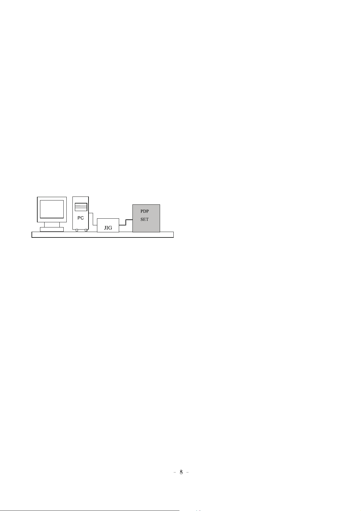
7. DDC Data Input
7-1. Required Test Equipment
(1) A jig for adjusting PC, DDC. (PC serial to D-sub.
Connection equipment)
(2) S/W for writing DDC(EDID data write & read)
(3) D-Sub 15P cable, D-Sub to DVI Connector (Connect to
DVI Jack)
7-2. Setting of Device
7-3. Preparation for Adjustment
(1) Set devices as above and turn the PC, jig on.
(2) Put S/W for writing DDC (EDID data write & read) into
operation. (operated in DOS mode.)
7-4. Sequence of Adjustment
(1) DDC Data Input for Analog-RGB
1) Put the set on the table and turn the power on.
2) Connect PC Serial to D-sub 15P Cable of JIG for DDC
Adjustment to RGB1 terminal (D-Sub 15Pin).
3) Operate S/W for DDC record and select DDC Data for
Analog RGB in Model Menu.
4) Operate EDID Write command.
5) Operate EDID Read command and check whether
Check Sum is OK.
6) If Check Sum is NG, repeat 3) ~ 4).
7) If Check Sum is OK, DDC Data for Analog-RGB input is
completed.
(2) DDC Data input for Digital-RGB
1) Connect PC Serial to DVI Cable of JIG for DDC
Adjustment to RGB2 terminal (DVI Jack).
2) Operate S/W for DDC record and select DDC Data for
Digital RGB in Model Menu.
3) Operate EDID Write command.
4) Operate EDID Read command and check whether
Check Sum is OK.
5) If Check Sum is NG, repeat 3) ~ 4).
6) If Check Sum is OK, DDC Data for Digital-RGB input is
completed.
8. Component Off-Set adjustment
Input the signal to HD-STB(SK-010T) and receive 14Ch.
8-1. Required Equipment
HD-STB (SK-010T or same product)
8-2. Manual Adjustment of Off-Set
(1) Input Video signal and Component 720P, 1080i signal of
HD-STB into AV1 and Component input part.
(2) Select Twin Picture by pressing ADJ twice on R/C, check
component in the main picture and AV1 in the sub picture.
(3) Adjust the R-OFFSET, B-OFFSET color impression of
component(Main picture) and external Input(Sub picture)
same by pressing Volume +,- key.
Page 9

BLOCK DIAGRAM
Page 10

EXPLODED VIEW
301
303
200
204
213
302
300
305
214
215
610
101
520
560
530
401
570
400
410
310
320
330
581
580
550
540
590
591
212
209
207
202
201
205
210
208
203
211
206
Page 11

EXPLODED VIEW PARTS LIST
101 5900V12001A FAN,DC G1225S12B2
200 6348Q-C030C PDP,50” 16:9 1365*768 DUAL SCAN PO
201 6871QCH019A PCB ASSEMBLY,CTRL ASSY HAND INSERT 50INCH V
202 6871QDH030A PCB ASSEMBLY,YDRV ASSY HAND INSERT 50WX1 4
203 6871QDH031A PCB ASSEMBLY,YDRV ASSY HAND INSERT 50WX1 4
204 6871QLH018A PCB ASSEMBLY,XRLT ASSY HAND INSERT 50WX1 4L
205 6871QLH019A PCB ASSEMBLY,XRLT ASSY HAND INSERT 50WX1 4L
206 6871QPH006A PCB ASSEMBLY,DCDC ASSY HAND INSERT 50WX1
207 6871QRH016A PCB ASSEMBLY,XRRT ASSY HAND INSERT 50WX1 4L
208 6871QRH017A PCB ASSEMBLY,XRRT ASSY HAND INSERT 50WX1 4L
209 6871QXH011A PCB ASSEMBLY,XRCT ASSY HAND INSERT 50WX1 4L
210 6871QXH012A PCB ASSEMBLY,XRCT ASSY HAND INSERT 50WX1 4L
211 6871QYH020A PCB ASSEMBLY,YSUS ASSY HAND INSERT 50WX1 4
212 6871QZH021A PCB ASSEMBLY,ZSUS ASSY HAND INSERT 50WX1 2
213 4980V00416A SUPPORTER ASSY,MN-50PZ40 RIGHT
214 4980V00416B SUPPORTER ASSY,MN-50PZ40 LEFT
215 4980V00498B SUPPORTER ASSY,AL SMPS DELTA
300 3091V00433B CABINET ASSEMBLY,LG FLATRON PLASMA
3091V00433F CABINET ASSEMBLY,MU-50PZ41B STEREO RF
301 4980V00361A SUPPORTER,FILTER TOP MN-50PZ40
302 4980V00362A SUPPORTER,FILTER BOTTOM MN-50PZ40
303 4980V00363A SUPPORTER,FILTER SIDE MN-50PZ40
305 3790V00683A WINDOW,GLASS FILTER MN50PZ41 MESH 110
310 5020V00688A BUTTON,CONTROL MN-50PZ41 SET
5020V00688B BUTTON,CONTROL MU-50PZ41B
320 320-062H SPRING,COIL
330 5020V00645A BUTTON,POWER OUTER MN-50PZ40 SET
5020V00645B BUTTON,POWER OUTER MU-50PZ41B
400 3809V00292A BACK COVER ASSEMBLY,MN-50PZ40 INNER
401 3301V00009D PLATE ASSEMBLY,AV MU-50PZ41
410 3809V00293B BACK COVER ASSEMBLY
3809V00293C BACK COVER ASSEMBLY,MU-50PZ41B
520 6871VMMN95A PCB ASSEMBLY,MAIN RF-02KE FOR MU PIVOT MODE
530 6871VSMD10A PCB ASSEMBLY,EXTRA RF-02CA 50IN IF/FIX
540 6871VSMD04A PCB ASSEMBLY,INTER RF-02CA I/F NTSC
550 6871VSMD06A PCB ASSEMBLY,A/V RF-02CA 50IN AUDIO
560 6871VSMD11A PCB ASSEMBLY,SPK RF-02CA 50IN RIGHT SPK
561 4980V00384A SUPPORTER,SPK AL INTERFACE,MN-50PZ40
570 3141VSNA57A CHASSIS ASSEMBLY,SUB RF-02CA PRE AMP
580 6871VSMD08A PCB ASSEMBLY,SUB KBD RF-02CA 50IN LOCAL KEY
581 5020V00647A BUTTON,CONTROL S/W INNER MN-50PZ40 SE
590 6871VSMD09A PCB ASSEMBLY,SUB PSW RF-02CA 50IN POWER SWITCH
591 5020V00648A BUTTON,POWER INNER MN-50PZ40 SET
600 6871VSMN17A PCB ASSEMBLY,SUB EXTRA RF02CA RF-02CA FAN CONTR
610 3501V00084C BOARD ASSEMBLY,POWER BOARD MU50PZ41 RF02KA SO
No.
Part No.
Description
Page 12

REPLACEMENT PARTS LIST
LOCA. NO PART NO DESCRIPTION
IC803
IC850
IC851
IC852
IC853
IC854
IC7
IC8
IC105
IC106
Q001
Q002
Q104
Q150
Q151
Q152
Q153
Q155
Q156
Q157
Q158
Q161
Q162
Q300
Q301
Q302
Q303
Q304
Q305
Q306
Q307
Q308
Q309
Q310
Q314
Q315
Q316
Q317
Q318
Q319
Q320
Q400
Q401
Q402
Q403
Q404
Q405
0IMCRFA010A
0IMCRRH001A
0IMCRRH001A
0IMCRRH001A
0IMCRRH001A
0IMCRRH001A
0TR830009BA
0TR830009BA
0TR830009BA
0TR830009BA
0TR387500AA
0TR387500AA
0TR387500AA
0TR387500AA
0TR387500AA
0TR387500AA
0TR387500AA
0TR387500AA
0TR387500AA
0TR387500AA
0TR387500AA
0TR150400BA
0TR150400BA
0TR150400BA
0TR150400BA
0TR387500AA
0TR150400BA
0TR150400BA
0TR150400BA
0TR387500AA
0TR150400BA
0TR387500AA
0TR387500AA
0TR150400BA
0TR387500AA
0TR387500AA
0TR150400BA
0TR387500AA
0TR150400BA
0TR387500AA
0TR387500AA
0TR387500AA
0TR387500AA
0TR387500AA
0TR150400BA
0TR387500AA
0TR104009AF
KA7809R, FAIRCHILD 2P D-PAK, R
BA033FP ROHM 3P-SOP,TO252-3 R/
BA033FP ROHM 3P-SOP,TO252-3 R/
BA033FP ROHM 3P-SOP,TO252-3 R/
BA033FP ROHM 3P-SOP,TO252-3 R/
BA033FP ROHM 3P-SOP,TO252-3 R/
BSS83 TP PHILIPS NON N-CHANNEL
BSS83 TP PHILIPS NON N-CHANNEL
BSS83 TP PHILIPS NON N-CHANNEL
BSS83 TP PHILIPS NON N-CHANNEL
CHIP 2SC3875S(ALY) KEC
CHIP 2SC3875S(ALY) KEC
CHIP 2SC3875S(ALY) KEC
CHIP 2SC3875S(ALY) KEC
CHIP 2SC3875S(ALY) KEC
CHIP 2SC3875S(ALY) KEC
CHIP 2SC3875S(ALY) KEC
CHIP 2SC3875S(ALY) KEC
CHIP 2SC3875S(ALY) KEC
CHIP 2SC3875S(ALY) KEC
CHIP 2SC3875S(ALY) KEC
CHIP 2SA1504S(ASY) KEC
CHIP 2SA1504S(ASY) KEC
CHIP 2SA1504S(ASY) KEC
CHIP 2SA1504S(ASY) KEC
CHIP 2SC3875S(ALY) KEC
CHIP 2SA1504S(ASY) KEC
CHIP 2SA1504S(ASY) KEC
CHIP 2SA1504S(ASY) KEC
CHIP 2SC3875S(ALY) KEC
CHIP 2SA1504S(ASY) KEC
CHIP 2SC3875S(ALY) KEC
CHIP 2SC3875S(ALY) KEC
CHIP 2SA1504S(ASY) KEC
CHIP 2SC3875S(ALY) KEC
CHIP 2SC3875S(ALY) KEC
CHIP 2SA1504S(ASY) KEC
CHIP 2SC3875S(ALY) KEC
CHIP 2SA1504S(ASY) KEC
CHIP 2SC3875S(ALY) KEC
CHIP 2SC3875S(ALY) KEC
CHIP 2SC3875S(ALY) KEC
CHIP 2SC3875S(ALY) KEC
CHIP 2SC3875S(ALY) KEC
CHIP 2SA1504S(ASY) KEC
CHIP 2SC3875S(ALY) KEC
CHIP KRC104S SOT-23 TP KEC - -
LOCA. NO PART NO DESCRIPTION
IC1
IC2
IC3
IC4
IC5
IC6
IC101
IC101
IC101
IC102
IC102
ICN102
IC103
IC103
IC104
IC104
IC105
IC201
IC202
IC301
IC302
IC401
IC402
IC404
IC405
IC501
IC502
IC503
IC504
IC601
IC701
IC702
IC703
IC704
IC741
IC742
IC743
IC744
IC745
IC746
IC747
IC748
IC749
IC750
IC752
IC801
IC802
0IMI623200B
0IDS162100B
0ISS278050A
0ISH092100A
0ISH092100A
0ISS278120A
0IAL242110A
0IMCRMN002A
0ISO208900A
0IAL242110A
0IKE780800J
0IMCRFA010A
0IMCRTI003A
0ISH052100C
0IBB368200A
0IKE704200J
0ISA428200A
0IMCRAD003A
0IMCRS5003A
0IMMRNE002A
0ISA715100D
0IIT323000D
0IFA741230A
0IMCRG2001A
0ISS464323A
0IMCROT001A
0ISS464323A
0ISS464323A
0ISS464323A
0IS5160000A
0IMCRRS001A
0IMMRSS064A
0IMMRMR006A
0IAL241610A
0IMCRFA013A
0IMCRFA013A
0ITI745740M
0IMCRPH017A
0IPH740800L
0IMCRPH015A
0IMCRPH016A
0IMCRPH014A
0IKE702700D
0IDS232000A
0IMCRTI001A
0IMCRSJ001A
0IPRPML001A
M62320FP,I/O EXPANDER 16P SOP
DS1621V 8P SOIC ST THERMOSTAT
KA278R05 4P,TO-220F BK LOW DRO
PQ09RF21 4P 9V S/W REGULATOR -
PQ09RF21 4P 9V S/W REGULATOR -
KA278R12 4P,TO-220F BK LOW DRO
AT24C21-10SI-2.5 8P,SOP TP 1K
MSP3440G QA B6 MICRONAS 80 QFP
CXA2089Q 48QFP BK A/V SWITCH
AT24C21-10SI-2.5 8P,SOP TP 1K
KIA7808API 3 ST REGULATOR .
KA7809R, FAIRCHILD 2P D-PAK, R
SN74HCT08D TEXAS INSTRUMENT 16
PQ05RD21 4SIP ST REGULATOR
OPA3682E 16P SOP ST BUFFER AMP
KIA7042AF SOT-89 TP 4.2V VOLTA
LA4282 12S 2CHX10W AUDIO AMP
AD9888KS-140 ANALOG DEVICE 128
SIL169 CL100 SILICON IMAGE 100
UPD64083GF3BA NEC 100 QFP ST 3
LA7151M 10SOP R/TP AUDIO SW FD
VPC3230D QA B4 80P QFP TRAY SO
DM74LS123MX 16SOP TP DUAL RETR
FLI2200 SAGE 176P,QFP TRAY VID
K4S643232E(C)-TC/L60(70) (KM43
REMBRANT-1A OPLUS TECHNOLOGIES
K4S643232E(C)-TC/L60(70) (KM43
K4S643232E(C)-TC/L60(70) (KM43
K4S643232E(C)-TC/L60(70) (KM43
SII160 100 TQFP ST PANELLINK D
R8820LV RDC SEMICONDUCTOR LTD
K6R4016V1C-TC10 SAMSUNG ELECTR
COPY MX29LV160TTC-70 MACRONIX
AT24C16N-10SI 8P SOIC ST EEPRO
74LCX244MTC FAIRCHILD 20P TSSO
74LCX244MTC FAIRCHILD 20P TSSO
SN74HC574NSR 14P,SOP TP D-TYPE
74LVC574APW PHILIPS 20P SOT360
74LVT08D 14SOP R/TP LOW VOLTAG
74LVC32AD PHILIPS 14P SOT108-1
74LVC139D PHILIPS 16P SOT109-1
74LV132D PHILIPS 14P SOT108-1
KIA7027AF 3, SOT-89 TP RESET I
DS232AS 16P,SOP TP RS-232 DRIV
SN74HCT157D TEXAS INSTRUMENT 1
SC1565IST-1.8 SEMTECH 3P SOT22
MIC39100 MICREL 3P SOT223 R/TP
IC
TRANSISTOR
RUN DATE : 2002.9.27
Page 13

LOCA. NO PART NO DESCRIPTION
Q407
QA101
QA102
QA103
QA720
QA721
QA722
QA723
QA740
QN101
QN102
QN103
QN104
QN105
QN106
QN107
QN108
D1
D001
D100
D101
D102
D103
D104
D105
D106
D107
D108
D109
D110
D111
D112
D113
D114
D115
D117
D118
D119
D120
D121
D122
D123
D801
D802
D803
D850
D851
D852
D853
D854
0TR150400BA
0TR150400BA
0TR150400BA
0TR150400BA
0TR387500AA
0TR387500AA
0TR387500AA
0TR150400BA
0TR387500AA
0TR387500AA
0TR387500AA
0TR387500AA
0TR150400BA
0TR150400BA
0TR387500AA
0TR150400BA
0TR387500AA
0DD100009AM
0DL200000CA
0DD226239AA
0DD226239AA
0DD226239AA
0DD226239AA
0DD226239AA
0DD226239AA
0DD226239AA
0DD226239AA
0DD226239AA
0DD226239AA
0DD226239AA
0DD226239AA
0DD226239AA
0DD226239AA
0DD226239AA
0DD226239AA
0DD226239AA
0DD226239AA
0DD226239AA
0DD226239AA
0DD226239AA
0DD226239AA
0DD226239AA
0DD226239AA
0DD226239AA
0DD226239AA
0DD226239AA
0DD226239AA
0DD226239AA
0DD226239AA
0DD226239AA
CHIP 2SA1504S(ASY) KEC
CHIP 2SA1504S(ASY) KEC
CHIP 2SA1504S(ASY) KEC
CHIP 2SA1504S(ASY) KEC
CHIP 2SC3875S(ALY) KEC
CHIP 2SC3875S(ALY) KEC
CHIP 2SC3875S(ALY) KEC
CHIP 2SA1504S(ASY) KEC
CHIP 2SC3875S(ALY) KEC
CHIP 2SC3875S(ALY) KEC
CHIP 2SC3875S(ALY) KEC
CHIP 2SC3875S(ALY) KEC
CHIP 2SA1504S(ASY) KEC
CHIP 2SA1504S(ASY) KEC
CHIP 2SC3875S(ALY) KEC
CHIP 2SA1504S(ASY) KEC
CHIP 2SC3875S(ALY) KEC
EU1ZV(1) TP SANKEN
LED,SAM5670(DL-2LRG) BK Y-GREEN -
CHIP KDS226 SOT-23
CHIP KDS226 SOT-23
CHIP KDS226 SOT-23
CHIP KDS226 SOT-23
CHIP KDS226 SOT-23
CHIP KDS226 SOT-23
CHIP KDS226 SOT-23
CHIP KDS226 SOT-23
CHIP KDS226 SOT-23
CHIP KDS226 SOT-23
CHIP KDS226 SOT-23
CHIP KDS226 SOT-23
CHIP KDS226 SOT-23
CHIP KDS226 SOT-23
CHIP KDS226 SOT-23
CHIP KDS226 SOT-23
CHIP KDS226 SOT-23
CHIP KDS226 SOT-23
CHIP KDS226 SOT-23
CHIP KDS226 SOT-23
CHIP KDS226 SOT-23
CHIP KDS226 SOT-23
CHIP KDS226 SOT-23
CHIP KDS226 SOT-23
CHIP KDS226 SOT-23
CHIP KDS226 SOT-23
CHIP KDS226 SOT-23
CHIP KDS226 SOT-23
CHIP KDS226 SOT-23
CHIP KDS226 SOT-23
CHIP KDS226 SOT-23
LOCA. NO PART NO DESCRIPTION
D855
D857
DA101
DA102
DA103
DA104
DA105
DA106
DN111
LD300
LD460
LD461
LD740
LD741
LD742
LD743
LD804
LD805
LD806
ZD116
ZD201
ZD750
ZD751
ZD752
C2
C003
C4
C8
C11
C13
C14
C15
C16
C109
C110
C111
C112
C113
C114
C115
C119
C121
C123
C127
C134
C150
C154
C158
C179
C182
0DD226239AA
0DD226239AA
0DD184009AA
0DD184009AA
0DD184009AA
0DD184009AA
0DD226239AA
0DD226239AA
0DD226239AA
0DL233309AC
0DL233309AC
0DL233309AC
0DL233309AC
0DL233309AC
0DL233309AC
0DL233309AC
0DL233309AC
0DL233309AC
0DL233309AC
0DR050008AA
0DR050008AA
0DR050008AA
0DR050008AA
0DR050008AA
0CE106SF6DC
0CE476SF6DC
0CE106SF6DC
0CE476SF6DC
0CE477VF6DC
0CE476SF6DC
0CE105SK6DC
0CE105SK6DC
0CE105SK6DC
0CE107SF6DC
0CE107SF6DC
0CE107SF6DC
0CE107SF6DC
0CE107SF6DC
0CE107SF6DC
0CE107SF6DC
0CE477VF6DC
0CE477VF6DC
0CE477VF6DC
0CE476SF6DC
0CE476SF6DC
0CE476SF6DC
0CE476SF6DC
0CE476SF6DC
0CE476SF6DC
0CE476SF6DC
CHIP KDS226 SOT-23
CHIP KDS226 SOT-23
KDS184S CHIP 85V 300MA KEC TP
KDS184S CHIP 85V 300MA KEC TP
KDS184S CHIP 85V 300MA KEC TP
KDS184S CHIP 85V 300MA KEC TP
CHIP KDS226 SOT-23
CHIP KDS226 SOT-23
CHIP KDS226 SOT-23
LED,SAM2333 TP KWANG GREEN/RED GRE
LED,SAM2333 TP KWANG GREEN/RED GRE
LED,SAM2333 TP KWANG GREEN/RED GRE
LED,SAM2333 TP KWANG GREEN/RED GRE
LED,SAM2333 TP KWANG GREEN/RED GRE
LED,SAM2333 TP KWANG GREEN/RED GRE
LED,SAM2333 TP KWANG GREEN/RED GRE
LED,SAM2333 TP KWANG GREEN/RED GRE
LED,SAM2333 TP KWANG GREEN/RED GRE
LED,SAM2333 TP KWANG GREEN/RED GRE
SD05.TC R/TP SEMTECH SOD323 5V
SD05.TC R/TP SEMTECH SOD323 5V
SD05.TC R/TP SEMTECH SOD323 5V
SD05.TC R/TP SEMTECH SOD323 5V
SD05.TC R/TP SEMTECH SOD323 5V
10UF MVG 16V 20% R/TP(SMD) SMD
47UF MVG 16V M SMD R/TP
10UF MVG 16V 20% R/TP(SMD) SMD
47UF MVG 16V M SMD R/TP
470UF MV 16V 20% R/TP(SMD) SMD
47UF MVG 16V M SMD R/TP
1UF MVG 50V M SMD R/TP
1UF MVG 50V M SMD R/TP
1UF MVG 50V M SMD R/TP
100UF MVG 16V M SMD R/TP
100UF MVG 16V M SMD R/TP
100UF MVG 16V M SMD R/TP
100UF MVG 16V M SMD R/TP
100UF MVG 16V M SMD R/TP
100UF MVG 16V M SMD R/TP
100UF MVG 16V M SMD R/TP
470UF MV 16V 20% R/TP(SMD) SMD
470UF MV 16V 20% R/TP(SMD) SMD
470UF MV 16V 20% R/TP(SMD) SMD
47UF MVG 16V M SMD R/TP
47UF MVG 16V M SMD R/TP
47UF MVG 16V M SMD R/TP
47UF MVG 16V M SMD R/TP
47UF MVG 16V M SMD R/TP
47UF MVG 16V M SMD R/TP
47UF MVG 16V M SMD R/TP
CAPACITOR
For Capacitor & Resistors,
the charactors at 2nd and 3rd
digit in the P/No. means as
follows;
CC, CX, CK, CN : Ceramic
CQ : Polyestor
CE : Electrolytic
RD : Carbon Film
RS : Metal Oxide Film
RN : Metal Film
RF : Fusible
DIODE
Page 14

LOCA. NO PART NO DESCRIPTION
C185
C300
C303
C306
C311
C316
C320
C322
C344
C348
C400
C401
C408
C409
C411
C418
C420
C425
C426
C427
C436
C452
C464
C800
C805
C808
C812
C816
C817
C820
C822
C825
C827
C829
C832
C835
C838
C840
C842
C845
C848
C849
C851
C853
C856
C859
C862
C865
C867
C869
C872
C875
0CE476SF6DC
0CE476SF6DC
0CE476SF6DC
0CE476SF6DC
0CE106SF6DC
0CN105EJ56A
0CN105EJ56A
0CE106SF6DC
0CE106SF6DC
0CE106SF6DC
0CN105EJ56A
0CE106SF6DC
0CE106SF6DC
0CE107SF6DC
0CK224DF56A
0CK224DF56A
0CE106SF6DC
0CK224DF56A
0CK224DF56A
0CK224DF56A
0CK224DF56A
0CE106SF6DC
0CE476SF6DC
0CE477VF6DC
0CE477VF6DC
0CE227VF6DC
0CE477VF6DC
0CE477VF6DC
0CE106SF6DC
0CE107SF6DC
0CE107SF6DC
0CE107SF6DC
0CE227VF6DC
0CE227VF6DC
0CE476SF6DC
0CE476SF6DC
0CE476SF6DC
0CE107SF6DC
0CE107SF6DC
0CE476SF6DC
0CE476SF6DC
0CE477VF6DC
0CE477VF6DC
0CE477VF6DC
0CE107SF6DC
0CE107SF6DC
0CE107SF6DC
0CE107SF6DC
0CE227VF6DC
0CE227VF6DC
0CE476SF6DC
0CE476SF6DC
47UF MVG 16V M SMD R/TP
47UF MVG 16V M SMD R/TP
47UF MVG 16V M SMD R/TP
47UF MVG 16V M SMD R/TP
10UF MVG 16V 20% R/TP(SMD) SMD
1.0UF 3216 35V 10% R/TP X7R
1.0UF 3216 35V 10% R/TP X7R
10UF MVG 16V 20% R/TP(SMD) SMD
10UF MVG 16V 20% R/TP(SMD) SMD
10UF MVG 16V 20% R/TP(SMD) SMD
1.0UF 3216 35V 10% R/TP X7R
10UF MVG 16V 20% R/TP(SMD) SMD
10UF MVG 16V 20% R/TP(SMD) SMD
100UF MVG 16V M SMD R/TP
220000PF 2012 16V 10% R/TP X7R
220000PF 2012 16V 10% R/TP X7R
10UF MVG 16V 20% R/TP(SMD) SMD
220000PF 2012 16V 10% R/TP X7R
220000PF 2012 16V 10% R/TP X7R
220000PF 2012 16V 10% R/TP X7R
220000PF 2012 16V 10% R/TP X7R
10UF MVG 16V 20% R/TP(SMD) SMD
47UF MVG 16V M SMD R/TP
470UF MV 16V 20% R/TP(SMD) SMD
470UF MV 16V 20% R/TP(SMD) SMD
220UF MV 16V 20% R/TP(SMD) SMD
470UF MV 16V 20% R/TP(SMD) SMD
470UF MV 16V 20% R/TP(SMD) SMD
10UF MVG 16V 20% R/TP(SMD) SMD
100UF MVG 16V M SMD R/TP
100UF MVG 16V M SMD R/TP
100UF MVG 16V M SMD R/TP
220UF MV 16V 20% R/TP(SMD) SMD
220UF MV 16V 20% R/TP(SMD) SMD
47UF MVG 16V M SMD R/TP
47UF MVG 16V M SMD R/TP
47UF MVG 16V M SMD R/TP
100UF MVG 16V M SMD R/TP
100UF MVG 16V M SMD R/TP
47UF MVG 16V M SMD R/TP
47UF MVG 16V M SMD R/TP
470UF MV 16V 20% R/TP(SMD) SMD
470UF MV 16V 20% R/TP(SMD) SMD
470UF MV 16V 20% R/TP(SMD) SMD
100UF MVG 16V M SMD R/TP
100UF MVG 16V M SMD R/TP
100UF MVG 16V M SMD R/TP
100UF MVG 16V M SMD R/TP
220UF MV 16V 20% R/TP(SMD) SMD
220UF MV 16V 20% R/TP(SMD) SMD
47UF MVG 16V M SMD R/TP
47UF MVG 16V M SMD R/TP
LOCA. NO PART NO DESCRIPTION
C878
C892
C894
C897
C900
C903
C906
C908
C910
C931
C933
C935
C938
C941
C944
C947
C949
C951
C954
C957
C966
C975
C977
C980
C983
C986
C989
C992
CA101
CA102
CA104
CA105
CA106
CA107
CA108
CA109
CA110
CA111
CA112
CA113
CA114
CA115
CA116
CA117
CA118
CA119
CA120
CA121
CA122
CA125
CA126
CA127
0CE106SF6DC
0CE477VF6DC
0CE477VF6DC
0CE107SF6DC
0CE107SF6DC
0CE107SF6DC
0CE107SF6DC
0CE477VF6DC
0CE477VF6DC
0CE107SF6DC
0CE477VF6DC
0CE477VF6DC
0CE107SF6DC
0CE227VF6DC
0CE476SF6DC
0CE476SF6DC
0CE477VF6DC
0CE477VF6DC
0CE107SF6DC
0CE476SF6DC
0CE107SF6DC
0CE227VF6DC
0CE227VF6DC
0CE476SF6DC
0CE107SF6DC
0CE476SF6DC
0CE107SF6DC
0CE107SF6DC
0CE477DK618
0CE477DK618
0CE107DH618
0CE105SK6DC
0CE106SF6DC
0CQ6821N509
0CE107DH618
0CQ6821N509
0CE477DK618
0CE477DK618
0CE106SF6DC
181-120K
181-120K
0CE477DK618
0CE107DH618
0CE477DK618
0CQ1041N509
0CE227VF6DC
0CE106SF6DC
0CQ1041N509
0CE227VF6DC
0CE107SF6DC
0CE474SK6DC
0CE474SK6DC
10UF MVG 16V 20% R/TP(SMD) SMD
470UF MV 16V 20% R/TP(SMD) SMD
470UF MV 16V 20% R/TP(SMD) SMD
100UF MVG 16V M SMD R/TP
100UF MVG 16V M SMD R/TP
100UF MVG 16V M SMD R/TP
100UF MVG 16V M SMD R/TP
470UF MV 16V 20% R/TP(SMD) SMD
470UF MV 16V 20% R/TP(SMD) SMD
100UF MVG 16V M SMD R/TP
470UF MV 16V 20% R/TP(SMD) SMD
470UF MV 16V 20% R/TP(SMD) SMD
100UF MVG 16V M SMD R/TP
220UF MV 16V 20% R/TP(SMD) SMD
47UF MVG 16V M SMD R/TP
47UF MVG 16V M SMD R/TP
470UF MV 16V 20% R/TP(SMD) SMD
470UF MV 16V 20% R/TP(SMD) SMD
100UF MVG 16V M SMD R/TP
47UF MVG 16V M SMD R/TP
100UF MVG 16V M SMD R/TP
220UF MV 16V 20% R/TP(SMD) SMD
220UF MV 16V 20% R/TP(SMD) SMD
47UF MVG 16V M SMD R/TP
100UF MVG 16V M SMD R/TP
47UF MVG 16V M SMD R/TP
100UF MVG 16V M SMD R/TP
100UF MVG 16V M SMD R/TP
470UF STD 50V 20% FL TP 5
470UF STD 50V 20% FL TP 5
100UF STD 25V M FL TP5
1UF MVG 50V M SMD R/TP
10UF MVG 16V 20% R/TP(SMD) SMD
0.0068U 100V K POLY TP
100UF STD 25V M FL TP5
0.0068U 100V K POLY TP
470UF STD 50V 20% FL TP 5
470UF STD 50V 20% FL TP 5
10UF MVG 16V 20% R/TP(SMD) SMD
2200PF 4KV M E FMTW LEAD 4.5
2200PF 4KV M E FMTW LEAD 4.5
470UF STD 50V 20% FL TP 5
100UF STD 25V M FL TP5
470UF STD 50V 20% FL TP 5
0.1U 100V K POLY TP
220UF MV 16V 20% R/TP(SMD) SMD
10UF MVG 16V 20% R/TP(SMD) SMD
0.1U 100V K POLY TP
220UF MV 16V 20% R/TP(SMD) SMD
100UF MVG 16V M SMD R/TP
0.47UF MVG 50V M SMD R/TP
0.47UF MVG 50V M SMD R/TP
For Capacitor & Resistors,
the charactors at 2nd and 3rd
digit in the P/No. means as
follows;
CC, CX, CK, CN : Ceramic
CQ : Polyestor
CE : Electrolytic
RD : Carbon Film
RS : Metal Oxide Film
RN : Metal Film
RF : Fusible
Page 15

LOCA. NO PART NO DESCRIPTION
CA128
CA129
CA131
CA132
CA133
CA134
CA135
CA139
CA140
CA153
CA154
CA154
CA155
CA156
CA751
CN113
CN114
CN115
CN119
CN120
CN121
CN122
CN123
CN124
CN127
CN130
CN133
CN137
CN138
CN141
CN144
CN145
CN147
CN149
L800
L801
L803
P102
P103
P103A
P103B
P120
PN101
PN102
PN103
PN104
PN105
0CE335SK6DC
0CE107SF6DC
0CE106SF6DC
0CE474SK6DC
0CE474SK6DC
0CE106SF6DC
0CE106SF6DC
0CE106SF6DC
0CE107SF6DC
0CE107SF6DC
0CE476SF6DC
0CE476SF6DC
0CE106SF6DC
0CE476SF6DC
0CE105SK6DC
0CE476SF6DC
0CE476SF6DC
0CE476SF6DC
0CE105SK6DC
0CE105SK6DC
0CE105SK6DC
0CE105SK6DC
0CE105SK6DC
0CE476SF6DC
0CE105SK6DC
0CE105SK6DC
0CE105SK6DC
0CE476SF6DC
0CE105SK6DC
0CE476SF6DC
0CE476SF6DC
0CE476SF6DC
0CE476SF6DC
0CE476SF6DC
6140VB0004B
6140VB0004B
150-C02F
380-068B
6612BBBHN6A
6612VLH001A
6612VLH001A
380-068B
380-363J
6612JH003CA
6612VMV002A
6612J00010A
6612JH003CA
3.3UF MVG 50V 20% SMD R/TP
100UF MVG 16V M SMD R/TP
10UF MVG 16V 20% R/TP(SMD) SMD
0.47UF MVG 50V M SMD R/TP
0.47UF MVG 50V M SMD R/TP
10UF MVG 16V 20% R/TP(SMD) SMD
10UF MVG 16V 20% R/TP(SMD) SMD
10UF MVG 16V 20% R/TP(SMD) SMD
100UF MVG 16V M SMD R/TP
100UF MVG 16V M SMD R/TP
47UF MVG 16V M SMD R/TP
47UF MVG 16V M SMD R/TP
10UF MVG 16V 20% R/TP(SMD) SMD
47UF MVG 16V M SMD R/TP
1UF MVG 50V M SMD R/TP
47UF MVG 16V M SMD R/TP
47UF MVG 16V M SMD R/TP
47UF MVG 16V M SMD R/TP
1UF MVG 50V M SMD R/TP
1UF MVG 50V M SMD R/TP
1UF MVG 50V M SMD R/TP
1UF MVG 50V M SMD R/TP
1UF MVG 50V M SMD R/TP
47UF MVG 16V M SMD R/TP
1UF MVG 50V M SMD R/TP
1UF MVG 50V M SMD R/TP
1UF MVG 50V M SMD R/TP
47UF MVG 16V M SMD R/TP
1UF MVG 50V M SMD R/TP
47UF MVG 16V M SMD R/TP
47UF MVG 16V M SMD R/TP
47UF MVG 16V M SMD R/TP
47UF MVG 16V M SMD R/TP
47UF MVG 16V M SMD R/TP
COIL,CHOKE 26UH 1UEWPHY 22.5TURN
COIL,CHOKE 26UH 1UEWPHY 22.5TURN
COIL,CHOKE 82UH PHY TURN
JACK,PHONE 3.5 EARPHONE WITH SW S
JACK,DIN 440062-1 AMP DVI INTERACED RIG
JACK,RCA SP022B 2P BK/R
JACK,RCA SP022B 2P BK/R
JACK,PHONE 3.5 EARPHONE WITH SW S
JACK,DIN PJ6046F H=8.0 W/O S/W
JACK,RCA PPJ137A AUDIO L-MON
JACK,DRAWING UCT-EX-020 UGCOM BNC MONO
JACK,RCA PPJ128A-1 A/V 2P MONO
JACK,RCA PPJ137A AUDIO L-MON
LOCA. NO PART NO DESCRIPTION
P1
P2
P101
P104
P741
AR200
AR201
AR202
AR203
AR204
AR205
AR206
AR207
AR208
AR209
AR210
AR211
AR260
AR261
AR262
AR263
AR264
AR265
AR266
AR267
AR268
AR269
AR270
AR271
AR400
AR401
AR402
AR403
AR460
AR461
AR462
AR463
AR464
AR465
AR466
AR467
AR468
AR469
AR470
AR471
AR472
AR473
AR474
387-B04J
387-A03J
6630VGA001C
6630VGA001C
6630VGA004B
0RRZVTA001D
0RRZVTA001D
0RRZVTA001D
0RRZVTA001D
0RRZVTA001D
0RRZVTA001D
0RRZVTA001D
0RRZVTA001D
0RRZVTA001D
0RRZVTA001D
0RRZVTA001D
0RRZVTA001D
0RRZVTA001D
0RRZVTA001D
0RRZVTA001D
0RRZVTA001D
0RRZVTA001D
0RRZVTA001D
0RRZVTA001D
0RRZVTA001D
0RRZVTA001D
0RRZVTA001D
0RRZVTA001D
0RRZVTA001D
0RRZVTA001D
0RRZVTA001D
0RRZVTA001D
0RRZVTA001D
0RRZVTA001D
0RRZVTA001D
0RRZVTA001D
0RRZVTA001D
0RRZVTA001D
0RRZVTA001D
0RRZVTA001D
0RRZVTA001D
0RRZVTA001D
0RRZVTA001D
0RRZVTA001D
0RRZVTA001D
0RRZVTA001D
0RRZVTA001D
0RRZVTA001D
CONNECTOR ASSY,4P SHIELD WIRE (L=500)
CONNECTOR ASSEMBLY,3P 500MM
CONNECTOR,D-SUB 15PIN 2.29MM
CONNECTOR,D-SUB 15PIN 2.29MM
CONNECTOR,D-SUB 9P 2.77MM FOR
22 OHM 1 / 16 W 1608 5% R/TP 4
22 OHM 1 / 16 W 1608 5% R/TP 4
22 OHM 1 / 16 W 1608 5% R/TP 4
22 OHM 1 / 16 W 1608 5% R/TP 4
22 OHM 1 / 16 W 1608 5% R/TP 4
22 OHM 1 / 16 W 1608 5% R/TP 4
22 OHM 1 / 16 W 1608 5% R/TP 4
22 OHM 1 / 16 W 1608 5% R/TP 4
22 OHM 1 / 16 W 1608 5% R/TP 4
22 OHM 1 / 16 W 1608 5% R/TP 4
22 OHM 1 / 16 W 1608 5% R/TP 4
22 OHM 1 / 16 W 1608 5% R/TP 4
22 OHM 1 / 16 W 1608 5% R/TP 4
22 OHM 1 / 16 W 1608 5% R/TP 4
22 OHM 1 / 16 W 1608 5% R/TP 4
22 OHM 1 / 16 W 1608 5% R/TP 4
22 OHM 1 / 16 W 1608 5% R/TP 4
22 OHM 1 / 16 W 1608 5% R/TP 4
22 OHM 1 / 16 W 1608 5% R/TP 4
22 OHM 1 / 16 W 1608 5% R/TP 4
22 OHM 1 / 16 W 1608 5% R/TP 4
22 OHM 1 / 16 W 1608 5% R/TP 4
22 OHM 1 / 16 W 1608 5% R/TP 4
22 OHM 1 / 16 W 1608 5% R/TP 4
22 OHM 1 / 16 W 1608 5% R/TP 4
22 OHM 1 / 16 W 1608 5% R/TP 4
22 OHM 1 / 16 W 1608 5% R/TP 4
22 OHM 1 / 16 W 1608 5% R/TP 4
22 OHM 1 / 16 W 1608 5% R/TP 4
22 OHM 1 / 16 W 1608 5% R/TP 4
22 OHM 1 / 16 W 1608 5% R/TP 4
22 OHM 1 / 16 W 1608 5% R/TP 4
22 OHM 1 / 16 W 1608 5% R/TP 4
22 OHM 1 / 16 W 1608 5% R/TP 4
22 OHM 1 / 16 W 1608 5% R/TP 4
22 OHM 1 / 16 W 1608 5% R/TP 4
22 OHM 1 / 16 W 1608 5% R/TP 4
22 OHM 1 / 16 W 1608 5% R/TP 4
22 OHM 1 / 16 W 1608 5% R/TP 4
22 OHM 1 / 16 W 1608 5% R/TP 4
22 OHM 1 / 16 W 1608 5% R/TP 4
22 OHM 1 / 16 W 1608 5% R/TP 4
22 OHM 1 / 16 W 1608 5% R/TP 4
For Capacitor & Resistors,
the charactors at 2nd and 3rd
digit in the P/No. means as
follows;
CC, CX, CK, CN : Ceramic
CQ : Polyestor
CE : Electrolytic
RD : Carbon Film
RS : Metal Oxide Film
RN : Metal Film
RF : Fusible
JACK
COIL
CONNECTOR
RESISTOR
Page 16

LOCA. NO PART NO DESCRIPTION
AR475
AR500
AR501
AR502
AR503
AR504
AR505
AR506
AR507
AR508
AR509
AR510
AR511
AR512
AR513
AR514
AR515
AR516
AR517
AR550
AR551
AR552
AR553
R22
RA101
RA102
RA105
RA109
RA114
RA117
SW001
SW002
SW003
SW004
SW005
SW006
SW101
SW742
SW800
IC106
IC107
IC108
L100
L101
L135
L136
L137
L138
0RRZVTA001D
0RRZVTA001D
0RRZVTA001D
0RRZVTA001D
0RRZVTA001D
0RRZVTA001D
0RRZVTA001D
0RRZVTA001D
0RRZVTA001D
0RRZVTA001D
0RRZVTA001D
0RRZVTA001D
0RRZVTA001D
0RRZVTA001D
0RRZVTA001D
0RRZVTA001D
0RRZVTA001D
0RRZVTA001D
0RRZVTA001D
0RRZVTA001C
0RRZVTA001C
0RRZVTA001C
0RRZVTA001C
0RD0152H609
0RS2701K607
0RS2701K607
0RD4700H609
0RD4700H609
0RS0221H609
0RS0221H609
140-315A
140-315A
140-315A
140-315A
140-315A
140-315A
140-275A
140-275A
6600VM2006A
6200VJS001A
6200VJS001A
6200VJS001A
6210VC0005A
6210VC0005A
6200JB8007L
6200JB8007L
6200JB8007L
6200JB8007L
22 OHM 1 / 16 W 1608 5% R/TP 4
22 OHM 1 / 16 W 1608 5% R/TP 4
22 OHM 1 / 16 W 1608 5% R/TP 4
22 OHM 1 / 16 W 1608 5% R/TP 4
22 OHM 1 / 16 W 1608 5% R/TP 4
22 OHM 1 / 16 W 1608 5% R/TP 4
22 OHM 1 / 16 W 1608 5% R/TP 4
22 OHM 1 / 16 W 1608 5% R/TP 4
22 OHM 1 / 16 W 1608 5% R/TP 4
22 OHM 1 / 16 W 1608 5% R/TP 4
22 OHM 1 / 16 W 1608 5% R/TP 4
22 OHM 1 / 16 W 1608 5% R/TP 4
22 OHM 1 / 16 W 1608 5% R/TP 4
22 OHM 1 / 16 W 1608 5% R/TP 4
22 OHM 1 / 16 W 1608 5% R/TP 4
22 OHM 1 / 16 W 1608 5% R/TP 4
22 OHM 1 / 16 W 1608 5% R/TP 4
22 OHM 1 / 16 W 1608 5% R/TP 4
22 OHM 1 / 16 W 1608 5% R/TP 4
4.7K OHM 1 / 16 W 1608 5% R/TP
4.7K OHM 1 / 16 W 1608 5% R/TP
4.7K OHM 1 / 16 W 1608 5% R/TP
4.7K OHM 1 / 16 W 1608 5% R/TP
15 OHM 1/2 W 5.00% TA52
2.7K OHM 2 W 5.00% TA62
2.7K OHM 2 W 5.00% TA62
470 OHM 1/2 W 5.00% TA52
470 OHM 1/2 W 5.00% TA52
2.2 OHM 1/2 W 5.00% TA52
2.2 OHM 1/2 W 5.00% TA52
SWITCH,TACT SKHV17910B NON 12V
SWITCH,TACT SKHV17910B NON 12V
SWITCH,TACT SKHV17910B NON 12V
SWITCH,TACT SKHV17910B NON 12V
SWITCH,TACT SKHV17910B NON 12V
SWITCH,TACT SKHV17910B NON 12V
SWITCH,PUSH JDPB21SA NON 30V 0
SWITCH,PUSH JDPB21SA NON 30V 0
SWITCH,PUSH SDDF3PATP011 UNIVERSAL
FILTER,EMC ZJY51R5-4P TDK DC 50VOLT 2A
FILTER,EMC ZJY51R5-4P TDK DC 50VOLT 2A
FILTER,EMC ZJY51R5-4P TDK DC 50VOLT 2A
FILTER,EMC BK2125 HS 750
FILTER,EMC BK2125 HS 750
FILTER,EMC HH2012 1M221JT
FILTER,EMC HH2012 1M221JT
FILTER,EMC HH2012 1M221JT
FILTER,EMC HH2012 1M221JT
LOCA. NO PART NO DESCRIPTION
L150
L300
L301
L302
L460
L806
L807
L808
L809
L810
L811
L850
L851
L852
L853
L854
L855
L856
L857
L858
L859
L860
L861
L862
L863
L864
L865
L866
L867
L868
L871
L872
L873
L874
L875
L876
L877
L880
L882
L883
L884
L885
L886
L887
L889
LA101
LA102
LA104
LA105
LA106
LN107
LN108
6210VC0006A
6210VC0005A
6210VC0005A
6210VC0005A
6210VC0006A
6210VC0006A
6210VC0006A
6210VC0006A
6210VC0006A
6210VC0006A
6210VC0006A
6210VC0006A
6210VC0006A
6210VC0006A
6210VC0006A
6210VC0006A
6210VC0006A
6210VC0006A
6210VC0006A
6210VC0006A
6210VC0006A
6210VC0006A
6210VC0006A
6210VC0006A
6210VC0006A
6210VC0006A
6210VC0006A
6210VC0006A
6210VC0006A
6210VC0006A
6210VC0006A
6210VC0006A
6210VC0006A
6210VC0006A
6210VC0006A
6210VC0006A
6210VC0006A
6210VC0006A
6210VC0006A
6210VC0006A
6210VC0006A
6210VC0006A
6210VC0006A
6210VC0006A
6210VC0006A
150-F09A
6210VC0006A
6210VC0006A
6210VC0006A
6210VC0006A
6210VC0006A
6210VC0006A
FILTER,EMC FBMH3216 HM501NT
FILTER,EMC BK2125 HS 750
FILTER,EMC BK2125 HS 750
FILTER,EMC BK2125 HS 750
FILTER,EMC FBMH3216 HM501NT
FILTER,EMC FBMH3216 HM501NT
FILTER,EMC FBMH3216 HM501NT
FILTER,EMC FBMH3216 HM501NT
FILTER,EMC FBMH3216 HM501NT
FILTER,EMC FBMH3216 HM501NT
FILTER,EMC FBMH3216 HM501NT
FILTER,EMC FBMH3216 HM501NT
FILTER,EMC FBMH3216 HM501NT
FILTER,EMC FBMH3216 HM501NT
FILTER,EMC FBMH3216 HM501NT
FILTER,EMC FBMH3216 HM501NT
FILTER,EMC FBMH3216 HM501NT
FILTER,EMC FBMH3216 HM501NT
FILTER,EMC FBMH3216 HM501NT
FILTER,EMC FBMH3216 HM501NT
FILTER,EMC FBMH3216 HM501NT
FILTER,EMC FBMH3216 HM501NT
FILTER,EMC FBMH3216 HM501NT
FILTER,EMC FBMH3216 HM501NT
FILTER,EMC FBMH3216 HM501NT
FILTER,EMC FBMH3216 HM501NT
FILTER,EMC FBMH3216 HM501NT
FILTER,EMC FBMH3216 HM501NT
FILTER,EMC FBMH3216 HM501NT
FILTER,EMC FBMH3216 HM501NT
FILTER,EMC FBMH3216 HM501NT
FILTER,EMC FBMH3216 HM501NT
FILTER,EMC FBMH3216 HM501NT
FILTER,EMC FBMH3216 HM501NT
FILTER,EMC FBMH3216 HM501NT
FILTER,EMC FBMH3216 HM501NT
FILTER,EMC FBMH3216 HM501NT
FILTER,EMC FBMH3216 HM501NT
FILTER,EMC FBMH3216 HM501NT
FILTER,EMC FBMH3216 HM501NT
FILTER,EMC FBMH3216 HM501NT
FILTER,EMC FBMH3216 HM501NT
FILTER,EMC FBMH3216 HM501NT
FILTER,EMC FBMH3216 HM501NT
FILTER,EMC FBMH3216 HM501NT
FILTER,EMC SQE2222 7-14MH 0.37PHY 48TURN
FILTER,EMC FBMH3216 HM501NT
FILTER,EMC FBMH3216 HM501NT
FILTER,EMC FBMH3216 HM501NT
FILTER,EMC FBMH3216 HM501NT
FILTER,EMC FBMH3216 HM501NT
FILTER,EMC FBMH3216 HM501NT
FILTER & CRYSTAL
For Capacitor & Resistors,
the charactors at 2nd and 3rd
digit in the P/No. means as
follows;
CC, CX, CK, CN : Ceramic
CQ : Polyestor
CE : Electrolytic
RD : Carbon Film
RS : Metal Oxide Film
RN : Metal Film
RF : Fusible
SWITCH
Page 17

LOCA. NO PART NO DESCRIPTION
LN109
LT300
LT301
LT302
R30
X300
X400
X601
X700
P001
A1
“
A2
A3
A4
A5
A6
6210VC0006A
6200C000010
6200C000010
6200C000009
6210VC0006A
6212AB2015B
6202VDT002E
156-A02M
6212AB2015C
6726VV0006K
3828VA0352K
3828VA0352C
6710V00084X
6410VUH005A
6612VMV002B
6850V00001A
6866VA9001B
FILTER,EMC FBMH3216 HM501NT
FILTER,B.P. H354LAI-K5202
FILTER,B.P. H354LAI-K5202
FILTER,B.P. H354LAI-K5225
FILTER,EMC FBMH3216 HM501NT
RESONATOR,CRYSTAL HC-49/SM5H 20MHZ +/- 30
RESONATOR,CRYSTAL SX-1SMD 20250000H
RESONATOR,CRYSTAL HC49U 18.432MHZ 30P
RESONATOR,CRYSTAL HC-49/SM4H 25MHZ +/- 50
REMOTE CONTROLLER RECEIVER,38KHZ
MANUAL,OWNERS RF02KE MU-50PZ41V LG EN/FR
MANUAL,OWNERS RF02KE MU-50PZ41VB
REMOTE CONTROLLER,MU-50PZ41 KEY
POWER CORD,PS204 125V/13A VOLEX UL/CSA 2
JACK,DRAWING UCT-EX-031 UGCOM BNC PLUG & RC
CABLE,FLAT 1566075-1 DVI A/D TO A/D 2000M
CONNECTOR (CIRC),D-SUB AWG 26 TWI 700
LOCA. NO PART NO DESCRIPTION
MISCELLANEOUS
ACCESSORIES
For Capacitor & Resistors,
the charactors at 2nd and 3rd
digit in the P/No. means as
follows;
CC, CX, CK, CN : Ceramic
CQ : Polyestor
CE : Electrolytic
RD : Carbon Film
RS : Metal Oxide Film
RN : Metal Film
RF : Fusible
Page 18

Sep., 200
Printed in KoreP/NO : 3828VD0121H
Page 19

Page 20

Page 21

Page 22

Page 23

Page 24

PRINTED CIRCUIT BOARD
MAIN(TOP)
MAIN(BOTTOM)
FAN CONTROL(TOP)
FAN CONTROL(BOTTOM)
PRE-AMP(TOP)
PRE-AMP(BOTTOM)
LOCAL KEY(TOP)
LOCAL KEY(BOTTOM)
POWER S/W(TOP)
POWER S/W(BOTTOM)
INTERFACE FIX(TOP)
INTERFACE FIX(BOTTOM)
RIGHT SPK(TOP)
RIGHT SPK(BOTTOM)
A/V NTSC(TOP)
A/V NTSC(BOTTOM)
AUDIO(TOP)
AUDIO(BOTTOM)
 Loading...