

LG MJW3281A, MJW3281AG, MJW1302A, MJW1302AG Service Manual
MJW3281A (NPN)
S
MJW1302A (PNP)
Preferred Devices
Complementary NPN−PNP
Silicon Power Bipolar
Transistors
The MJW3281A and MJW1302A are PowerBaset power
transistors for high power audio, disk head positioners and other linear
applications.
Features
• Designed for 100 W Audio Frequency
• Gain Complementary:
Gain Linearity from 100 mA to 7 A
hFE = 45 (Min) @ IC = 8 A
• Low Harmonic Distortion
• High Safe Operation Area − 1 A/100 V @ 1 Second
• High f
− 30 MHz Typical
T
• Pb−Free Packages are Available*
MAXIMUM RATINGS (T
Rating Symbol Value Unit
Collector−Emitter Voltage V
Collector−Base Voltage V
Emitter−Base Voltage V
Collector−Emitter Voltage − 1.5 V V
Collector Current − Continuous
Collector Current − Peak (Note 1)
Base Current − Continuous I
Total Power Dissipation @ TC = 25°C
Derate Above 25°C
Operating and Storage Junction
Temperature Range
THERMAL CHARACTERISTICS
Characteristic Symbol Max Unit
Thermal Resistance, Junction−to−Case
Thermal Resistance, Junction−to−Ambient
Maximum ratings are those values beyond which device damage can occur.
Maximum ratings applied to the device are individual stress limit values (not
normal operating conditions) and are not valid simultaneously. If these limits are
exceeded, device functional operation is not implied, damage may occur and
reliability may be affected.
1. Pulse Test: Pulse Width = 5 ms, Duty Cycle < 10%.
*For additional information on our Pb−Free strategy and soldering details, please
download the ON Semiconductor Soldering and Mounting Techniques
Reference Manual, SOLDERRM/D.
= 25°C unless otherwise noted)
J
CEO
CBO
EBO
CEX
I
C
B
P
D
TJ, T
R
R
stg
q
JC
q
JA
−65 to +150
230 Vdc
230 Vdc
5.0 Vdc
230 Vdc
15
25
1.5 Adc
200
1.43
0.625 °C/W
40 °C/W
Adc
W
W/°C
°C
http://onsemi.com
15 AMPERES
COMPLEMENTARY
SILICON POWER TRANSISTOR
230 VOLTS 200 WATTS
1
2
3
MARKING DIAGRAM
MJWxxxxA
AYWWG
1 BASE
2 COLLECTOR
xxxx = 3281 or 1302
A = Assembly Location
Y = Year
WW = Work Week
G = Pb−Free Package
ORDERING INFORMATION
Device Package Shipping
MJW3281A TO−247
MJW3281AG TO−247
MJW1302A TO−247 30 Units/Rail
MJW1302AG TO−247
Preferred devices are recommended choices for future use
and best overall value.
(Pb−Free)
(Pb−Free)
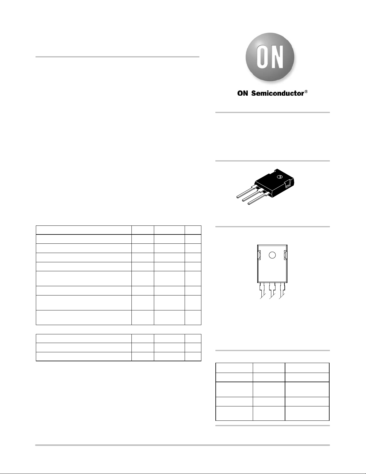
TO−247
CASE 340L
3 EMITTER
30 Units/Rail
30 Units/Rail
30 Units/Rail
© Semiconductor Components Industries, LLC, 2006
January, 2006 − Rev. 3
1 Publication Order Number:
MJW3281A/D
MJW3281A (NPN) MJW1302A (PNP)
ELECTRICAL CHARACTERISTICS (T
= 25°C unless otherwise noted)
C
Characteristic Symbol Min Typ Max Unit
OFF CHARACTERISTICS
Collector−Emitter Sustaining Voltage
(IC = 100 mAdc, IB = 0)
Collector Cutoff Current
(V
= 230 Vdc, IE = 0)
CB
Emitter Cutoff Current
(VEB = 5 Vdc, IC = 0)
SECOND BREAKDOWN
Second Breakdown Collector with Base Forward Biased
(VCE = 50 Vdc, t = 1 s (non−repetitive)
(VCE = 100 Vdc, t = 1 s (non−repetitive)
ON CHARACTERISTICS
DC Current Gain
(IC = 100 mAdc, VCE = 5 Vdc)
(IC = 1 Adc, VCE = 5 Vdc)
(IC = 3 Adc, VCE = 5 Vdc)
(IC = 5 Adc, VCE = 5 Vdc)
(IC = 7 Adc, VCE = 5 Vdc)
(IC = 8 Adc, VCE = 5 Vdc)
(IC = 15 Adc, VCE = 5 Vdc)
Collector−Emitter Saturation Voltage
(IC = 10 Adc, IB = 1 Adc)
Base−Emitter On Voltage
(IC = 8 Adc, VCE = 5 Vdc)
DYNAMIC CHARACTERISTICS
Current−Gain − Bandwidth Product
(IC = 1 Adc, VCE = 5 Vdc, f
= 1 MHz)
test
Output Capacitance
(VCB = 10 Vdc, IE = 0, f
= 1 MHz)
test
V
CEO(sus)
I
CBO
I
EBO
I
S/b
h
FE
V
CE(sat)
V
BE(on)
f
C
230 − −
Vdc
mAdc
− − 50
mAdc
− − 5
Adc
4
1
−
−
−
−
−
50
50
50
50
50
45
12
125
−
−
−
115
−
35
200
200
200
200
200
−
−
Vdc
− 0.4 2
Vdc
− − 2
T
ob
− 30 −
− − 600
MHz
pF
http://onsemi.com
2
 Loading...