

LG MJL3281A, MJL3281AG, MJL1302A, MJL1302AG Service Manual
MJL3281A (NPN)
MJL1302A (PNP)
Preferred Devices
Complementary Bipolar
Power Transistors
Features
• Exceptional Safe Operating Area
• NPN/PNP Gain Matching within 10% from 50 mA to 5 A
• Excellent Gain Linearity
• High BVCEO
• High Frequency
• Pb−Free Packages are Available
Benefits
• Reliable Performance at Higher Powers
• Symmetrical Characteristics in Complementary Configurations
• Accurate Reproduction of Input Signal
• Greater Dynamic Range
• High Amplifier Bandwith
Applications
• High−End Consumer Audio Products
♦Home Amplifiers
♦Home Receivers
• Professional Audio Amplifiers
♦Theater and Stadium Sound Systems
♦Public Address Systems (PAs)
MAXIMUM RATINGS (T
Rating
Collector−Emitter Voltage V
Collector−Base Voltage V
Emitter−Base Voltage V
Collector−Emitter Voltage − 1.5 V V
Collector Current − Continuous
Base Current − Continuous I
Total Power Dissipation @ TC = 25°C
Derate Above 25°C
Operating and Storage Junction
Temperature Range
THERMAL CHARACTERISTICS
Characteristic Symbol Max Unit
Thermal Resistance, Junction−to−Case R
Maximum ratings are those values beyond which device damage can occur.
Maximum ratings applied to the device are individual stress limit values (not
normal operating conditions) and are not valid simultaneously . If these limits are
exceeded, device functional operation is not implied, damage may occur and
reliability may be affected.
1. Pulse Test: Pulse Width = 5 ms, Duty Cycle < 10%.
= 25°C unless otherwise noted)
J
− Peak (Note 1)
Symbol Value Unit
stg
260 Vdc
260 Vdc
5.0 Vdc
260 Vdc
15
25
1.5 Adc
200
1.43
− 65 to
+150
0.625 °C/W
Adc
Watts
W/°C
°C
CEO
CBO
EBO
CEX
I
P
TJ, T
C
B
D
θ
JC
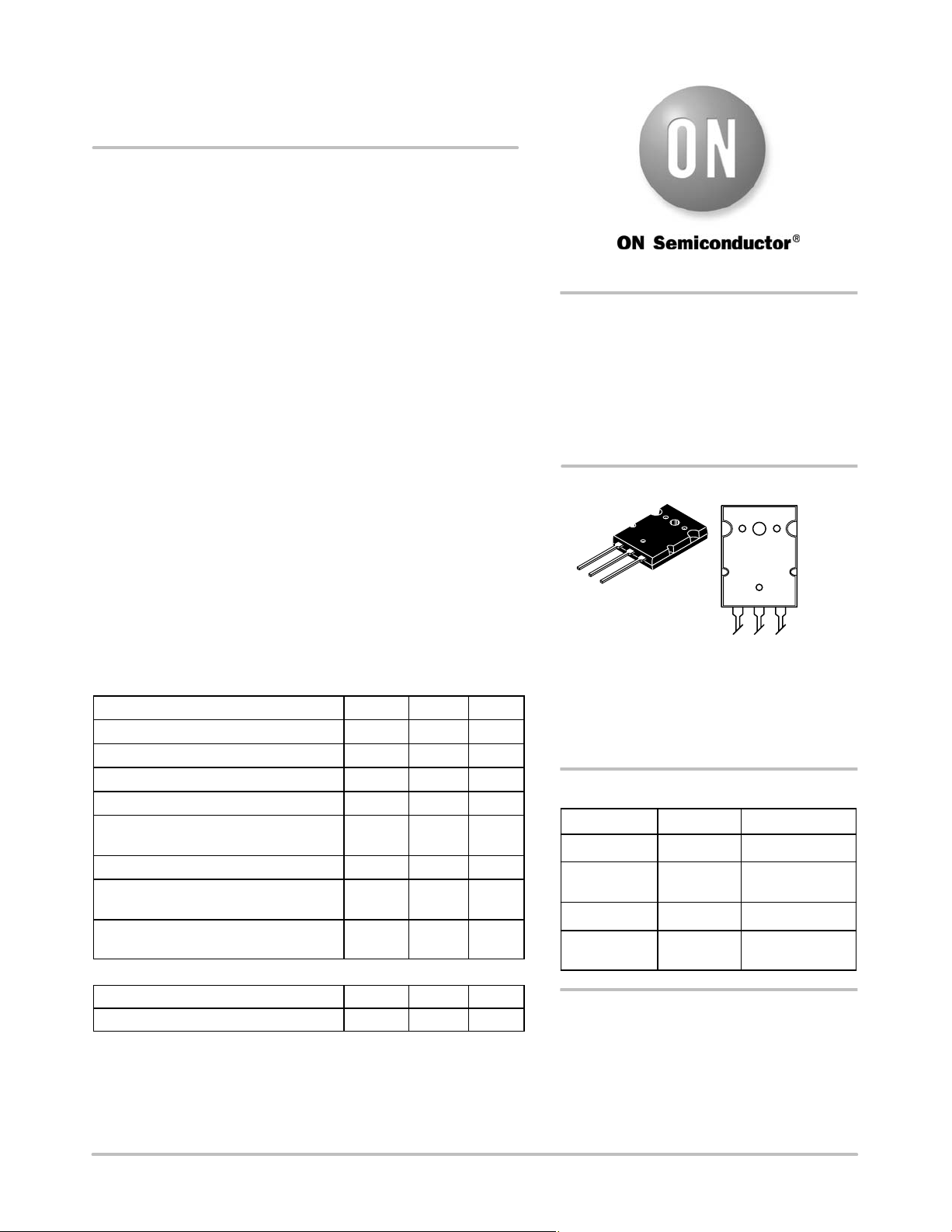
http://onsemi.com
15 AMPERES
COMPLEMENTARY
SILICON POWER
TRANSISTORS
260 VOLTS
200 WATTS
MARKING DIAGRAM
MJLxxxxA
1
BASE
2 COLLECTOR
AYYWWG
3
EMITTER
25 Units/Rail
25 Units/Rail
25 Units/Rail
1
2
3
TO−264
CASE 340G
STYLE 2
xxxx = 3281 or 1302
A = Location Code
YY = Year
WW = Work Week
G = Pb−Free Package
ORDERING INFORMATION
Device Package Shipping
MJL3281A TO−264
MJL3281AG TO−264
MJL1302A TO−264 25 Units/Rail
MJL1302AG TO−264
Preferred devices are recommended choices for future use
and best overall value.
(Pb−Free)
(Pb−Free)
© Semiconductor Components Industries, LLC, 2005
October, 2005 − Rev. 9
1 Publication Order Number:
MJL3281A/D
MJL3281A (NPN) MJL1302A (PNP)
ELECTRICAL CHARACTERISTICS (T
= 25°C unless otherwise noted)
C
Characteristic
OFF CHARACTERISTICS
Collector−Emitter Sustaining Voltage
(I
= 100 mAdc, IB = 0)
C
Collector Cutoff Current
= 260 Vdc, IE = 0)
(V
CB
Emitter Cutoff Current
(V
= 5 Vdc, IC = 0)
EB
SECOND BREAKDOWN
Second Breakdown Collector with Base Forward Biased
(V
= 50 Vdc, t = 1 s (non−repetitive)
CE
= 100 Vdc, t = 1 s (non−repetitive)
(V
CE
ON CHARACTERISTICS
DC Current Gain
(I
= 500 mAdc, VCE = 5 Vdc)
C
= 1 Adc, VCE = 5 Vdc)
(I
C
(I
= 3 Adc, VCE = 5 Vdc)
C
(I
= 5 Adc, VCE = 5 Vdc)
C
(I
= 8 Adc, VCE = 5 Vdc)
C
Collector−Emitter Saturation Voltage
(I
= 10 Adc, IB = 1 Adc)
C
DYNAMIC CHARACTERISTICS
Current−Gain − Bandwidth Product
(I
= 1 Adc, VCE = 5 Vdc, f
C
= 1 MHz)
test
Output Capacitance
(V
= 10 Vdc, IE = 0, f
CB
= 1 MHz)
test
Symbol Min Max Unit
V
CEO(sus)
Vdc
260 −
I
CBO
μAdc
− 50
I
EBO
μAdc
− 5
I
h
V
CE(sat)
S/b
FE
75
75
75
75
45
4
1
−
−
150
150
150
150
−
Adc
Vdc
− 3
f
T
MHz
30 −
C
ob
− 600
pF
http://onsemi.com
2
 Loading...