

LG MG300d Service Manual

Date: January, 2006 / Issue 1.0
Service Manual
Model : MG300d
Service Manual
MG300d
Z3X-BOX.COM

- 3 -
1. INTRODUCTION .............................. 5
1.1 Purpose................................................... 5
1.2 Regulatory Information............................ 5
1.3 Abbreviations .......................................... 7
2. PERFORMANCE.............................. 9
2.1 H/W Feature............................................ 9
2.2 RF Characteristics ................................ 15
2.3 Technical Specification ......................... 18
3. TECHNICAL BRIEF ....................... 23
3.1 Power Transceiver .................................23
3.2 13 MHz Clock.........................................30
3.3 Switchplexer for Triband ........................30
3.4 Digital Main Processor ...........................32
3.5 Analog Main & Power Management
Processor...............................................38
3.6 Chargind IC............................................46
3.7 CAMERA IC ...........................................49
3.8 MIDI IC...................................................51
3.9 Keypad Switches and Scanning ............55
3.10 Microphone ..........................................56
3.11 Main Speaker.......................................56
3.12 Headset Interface.................................57
3.13 MEMORY.............................................58
BLUETOOTH .......................................59
CAMERA CONNECTOR, CAMERA LDO ..60
FLASH LED CHARGE PUMP..............61
NAND MEMORY..................................62
FLIP SWITCH ......................................63
3.14 VIBRATOR...........................................64
4. TROUBLESHOOTING ................... 65
4.1 RX Trouble.............................................65
4.2 TX Trouble .............................................71
4.3 Power On Trouble..................................78
4.4 Charging Trouble ...................................80
4.5 Vibrator Trouble .....................................82
4.6 LCD Trouble...........................................84
4.7 BT Trouble .............................................87
4.8 Speaker Trouble ....................................90
4.9 SIM Card Interface Trouble....................92
4.10 Earphone Trouble ................................94
4.11 Receiver Trouble..................................96
4.12 Microphone Trouble .............................98
4.13 RTC Trouble ......................................100
5. DOWNLOAD AND CALIBRATION ..... 102
5.1 Download............................................ 102
5.2 Calibration........................................... 106
6. BLOCK DIAGRAM ....................... 113
7. CIRCUIT DIAGRAM ..................... 115
8. PCB LAYOUT............................... 125
9. ENGINEERING MODE ..................127
9.1 BB Test [MENU 1]................................128
9.2 RF Test [MENU 2]................................130
9.3 MF mode [MENU 3] .............................130
9.4 Trace option [MENU 4] ........................131
9.5 Call timer [MENU 5] .............................131
9.6 Fact. Reset [MENU 6] ..........................131
9.7 S/W version..........................................131
10. STAND ALONE TEST ................ 132
10.1 Introduction ........................................132
10.2 Setting Method...................................132
10.3 Means of Test ....................................133
Table Of Contents
Z3X-BOX.COM

- 4 -
11. AUTO CALIBRATION................. 135
11. AUTO CALIBRATION ..........................135
11.1 Overview ............................................135
11.2 Requirements.....................................135
11.3 Menu and Settings.............................135
11.4 AGC ...................................................137
11.5 APC....................................................137
11.6 ADC ...................................................137
11.7 Setting................................................137
11.8 How to do calibration .........................137
12. EXPLODED VIEW &
REPLACEMENT PART LIST ..... 140
12.1 EXPLODED VIEW ............................ 140
12.2 Replacement Parts
<Mechanic component>.................... 143
<Main component> ........................... 147
12.3 Accessory ......................................... 163
Z3X-BOX.COM

1. INTRODUCTION
- 5 -
1.1 Purpose
This manual provides the information necessary to repair, calibration, description and download the
features of this model.
1.2 Regulatory Information
A. Security
Toll fraud, the unauthorized use of telecommunications system by an unauthorized part (for example,
persons other than your company’s employees, agents, subcontractors, or person working on your
company’s behalf) can result in substantial additional charges for your telecommunications services.
System users are responsible for the security of own system. There are may be risks of toll fraud
associated with your telecommunications system. System users are responsible for programming and
configuring the equipment to prevent unauthorized use. The manufacturer does not warrant that this
product is immune from the above case but will prevent unauthorized use of common-carrier
telecommunication service of facilities accessed through or connected to it.
The manufacturer will not be responsible for any charges that result from such unauthorized use.
B. Incidence of Harm
If a telephone company determines that the equipment provided to customer is faulty and possibly
causing harm or interruption in service to the telephone network, it should disconnect telephone
service until repair can be done. A telephone company may temporarily disconnect service as long as
repair is not done.
C. Changes in Service
A local telephone company may make changes in its communications facilities or procedure. If these
changes could reasonably be expected to affect the use of the this phone or compatibility with the
network, the telephone company is required to give advanced written notice to the user, allowing the
user to take appropriate steps to maintain telephone service.
D. Maintenance Limitations
Maintenance limitations on this model must be performed only by the manufacturer or its authorized
agent.
The user may not make any changes and/or repairs expect as specifically noted in this manual.
Therefore, note that unauthorized alternations or repair may affect the regulatory status of the system
and may void any remaining warranty.
1. INTRODUCTION
Z3X-BOX.COM

1. INTRODUCTION
- 6 -
E. Notice of Radiated Emissions
This model complies with rules regarding radiation and radio frequency emission as defined by local
regulatory agencies. In accordance with these agencies, you may be required to provide information
such as the following to the end user.
F. Pictures
The pictures in this manual are for illustrative purposes only; your actual hardware may look slightly
different.
G. Interference and Attenuation
Phone may interfere with sensitive laboratory equipment, medical equipment, etc.Interference from
unsuppressed engines or electric motors may cause problems.
H. Electrostatic Sensitive Devices
ATTENTION
Boards, which contain Electrostatic Sensitive Device (ESD), are indicated by the sign.
Following information is ESD handling:
• Service personnel should ground themselves by using a wrist strap when exchange system boards.
• When repairs are made to a system board, they should spread the floor with anti-static mat which is
also grounded.
• Use a suitable, grounded soldering iron.
• Keep sensitive parts in these protective packages until these are used.
• When returning system boards or parts like EEPROM to the factory, use the protective package as
described.
Z3X-BOX.COM

1. INTRODUCTION
- 7 -
1.3 Abbreviations
For the purposes of this manual, following abbreviations apply:
APC Automatic Power Control
BB Baseband
BER Bit Error Ratio
CC-CV Constant Current - Constant Voltage
DAC Digital to Analog Converter
DCS Digital Communication System
dBm dB relative to 1 milli watt
DSP Digital Signal Processing
EEPROM Electrical Erasable Programmable Read-Only Memory
ESD Electrostatic Discharge
FPCB Flexible Printed Circuit Board
GMSK Gaussian Minimum Shift Keying
GPIB General Purpose Interface Bus
GSM Global System for Mobile Communications
IPUI International Portable User Identity
IF Intermediate Frequency
LCD Liquid Crystal Display
LDO Low Drop Output
LED Light Emitting Diode
OPLL Offset Phase Locked Loop
Z3X-BOX.COM

1. INTRODUCTION
- 8 -
PAM Power Amplifier Module
PCB Printed Circuit Board
PGA Programmable Gain Amplifier
PLL Phase Locked Loop
PSTN Public Switched Telephone Network
RF Radio Frequency
RLR Receiving Loudness Rating
RMS Root Mean Square
RTC Real Time Clock
SAW Surface Acoustic Wave
SIM Subscriber Identity Module
SLR Sending Loudness Rating
SRAM Static Random Access Memory
PSRAM Pseudo SRAM
STMR Side Tone Masking Rating
TA Travel Adapter
TDD Time Division Duplex
TDMA Time Division Multiple Access
UART Universal Asynchronous Receiver/Transmitter
VCO Voltage Controlled Oscillator
VCTCXO Voltage Control Temperature Compensated Crystal Oscillator
WAP Wireless Application Protocol
Z3X-BOX.COM

2. PERFORMANCE
- 9 -
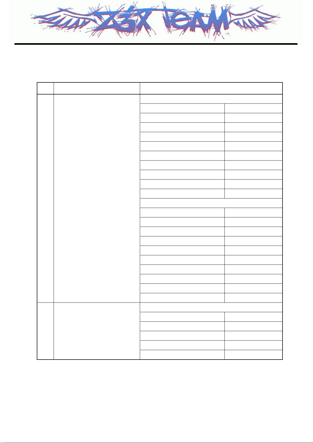
2.1 H/W Features
2. PERFORMANCE
Item Target Specification
Form Factor Clam Shell (Dual LCD)
Size 89.9 X 46.2 X 23 mm
Weight TBD
Battery 3.7V, 1000 mAh LI-Ion
Talk Time Up to 3h : GSM Tx Level 7
Standby Time Up to 200 hrs : Paging Period 9, RSSI 85dBm
Antenna Internal Antenna
LCD Main: 262K Colour 128*160 TFT / Sub: 65K Colour OLED 96*96
Camera Built-in CMOS 1.3M Pixels Camera
Back Light(Key Pad) LED
Back Light colour(Key) Blue
Vibrator Yes
Buzzer N/A
C-MIC Yes
Receiver Yes
Earphone Jack Yes / Jack
SIM Socket Yes (SIM Block Type) → 3V only
Volume Key Yes
Voice Key Yes
I/O Connect 24 Pin
Basic Accessory Travel Adaptor / Battery / Ear Phone + Mic Data Cable
Option N/A
Z3X-BOX.COM
2. PERFORMANCE
- 10 -
Function Target Specification
RSSI (5 Level)
Battery Charging (5 Level)
Display
RTC
Multi-Language (English, French, German, Spanish, Dutch, etc.)
Quick Access Mode(HOT KEY)
PLMN/Service Indicator
Number of Keys : 24 Key (including Soft key, side key)
Keypad
Soft Function Keys : 2
International Access (+)(long 0)
HotKey : OK,
Normal Features Last Dialled Number : 20
Last Received Number : 20
Last Missed Number : 10
Scratch Pad Memory(Save a phone number in call) : 1
Call Waiting
Call Swap
Call Retrieve
Any Key Answer
Auto Answer
Closed User Group
Call Management Automatic Redial
Calling Line Identification
Full Call divert
Speed Dialling
Last Number Redial
Multi-party Call (Conference Call)
Explicit Call Transfer
Voice Recording Voice Recording in idle (15 Sec/10 message)
Automatic Network Selection
Network Manual Network Selection
Network Service Status
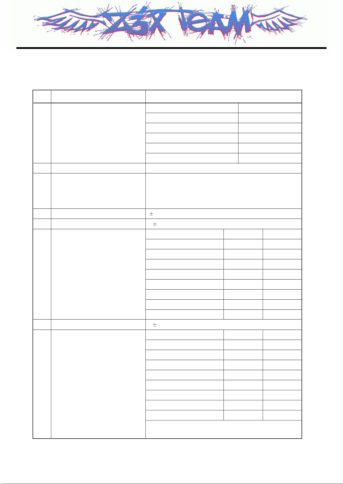
Z3X-BOX.COM
2. PERFORMANCE
- 11 -
Read Cell Broadcast
Cell Broadcast Cell Broadcast Categories
Cell Broadcast Message Language
Number Store and Recall
Alpha Store and Recall
Search the Phone Book in call
Scroll by alpha or number
Last Number Dialled (20)
Phone Book
Last Number Missed (10)
Last Number Received (20)
Copy & Move
Fixed Dial Number
Service Dial Number
Email Entry
Entry : 200 names
Last Call Timer
Last Call Charge Units
Call Cost Total Call Timer
Total Charge Units
Visible, Audible Call Time/Cost Indication
Key tone setting
Key / Ring Tone Volume (5 Level)
Ring Tone Pattern 20(fixed) + My Folder Ring tone 24(Default)
Audio Ring Type:
Silent / Vibrator & Ring / Ring only / Vibrator only/Ring after Vibrator
Earpiece Volume (5 Level)
Mute
DTMF
DTMF Signalling
DTMF Enable & Disable
Z3X-BOX.COM
2. PERFORMANCE
- 12 -
Call Forwarding All Incoming Calls
Call Forwarding On Busy
Call Forwarding No Reply
Call forwarding Not-reachable
Supplementary Services
Call Barring All Outgoing Calls
Call Barring All Outgoing International Calls
Call Barring All Outgoing int. Calls except to Home Country
Call Barring All incoming Calls
Call Barring All incoming Calls when roaming
Conference Call (up to 5 calls)
Plug-In Type : 3V Only
SIM
Service Provider Lock & Network Lock
SIM Toolkit (Class 1, 2, 3)
Prepaid SIM Operation
Read Message
Write and Edit Message
Send and Receive Message
Reply to Message
Forward Message
Extract Number from Message
Message Status
Short Message Message Unread Indicator
Settable Message Center Number,
Visible and Audible Message
Voice Mail
Settable Voice Mail Center Number
Message Protocol
Message Overflow Indicator
Message Center Number
Multi-Band Support of Multi-band & Mode
Development & Test Facility
Miscellaneous Function
Field Test Facility
Display Software Version
IMEI
Z3X-BOX.COM
2. PERFORMANCE
- 13 -
Text Input T9 (Predictive word input)
Organizer Scheduler & Calendar
World Time
Setting Local time
Number of Selectable Cities: 65
Unit converter Weight/Length/Square/Volume
Calculator Addition, Subtraction, Multiplication, Division
Edit, save and sending SMS on PC
Scheduler Sync
PC Sync Phone Book Sync
Internet Kit supporting PC OS (98,2000,ME,XP)
Contents D/Load (Wallpaper/Ringtone)
Data Circuit (up to 14.4kbps)
GPRS GPRS Multi slot Class 10
Game Java Download Games
Menu Quick Access Mode
Read Software Version
Handset Battery Charging Mode
Restore Factory Setting
Security
SIM Lock
Emergency Call
12/24 hour
Calendar with Automatic Leap Year Adjustment
Time Zone and Day Light Saving Adjustment
Real Time Clock
Alarm Manager
On Alarm Event
Display Message on Alarm Event
Others Profiles
Z3X-BOX.COM
2. PERFORMANCE
- 14 -
Read and Save MMS Message
Preview MMS Message
Send and Receive MMS Message
Previous, Next slide
MMS (3GPP R5)
Set timer
Remove media
Delete slide (up to 30 pages)
Attach MMS media (Text, Audio, Picture)
Audio: SP-MIDI, I-Melody (AMR: supported)
Picture: GIF87,GIF89a, PNG, JPEG, WBMP
WAP version 2.0 @ TELECA
JAVA MIDP 2.0 @ Esmertec
Z3X-BOX.COM

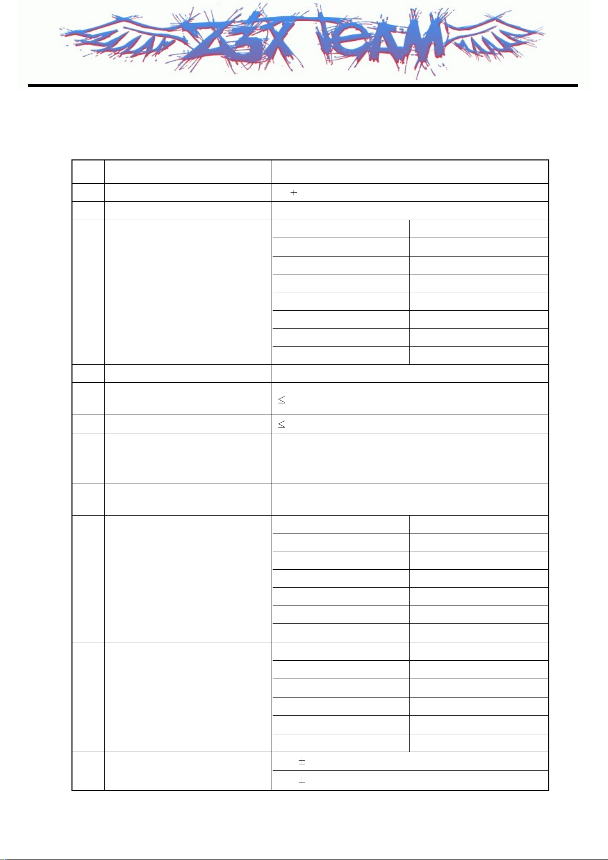
1) Transmitter
2. PERFORMANCE
- 15 -
2.2 RF Characteristics
NO Item GSM 850 DCS1800
100kHz ~ 1GHz -36dBm -36dBm
1GHz ~ 12.75GHz -30dBm
1GHz ~ 1710MHz -30dBm
1710MHz ~ 1785MHz -36dBm
1785MHz ~ 12.75GHz -30dBm
100kHz ~ 880MHz -57dBm -57dBm
880MHz ~ 915MHz -59dBm -59dBm
915MHz ~ 1GHz -57dBm -57dBm
1GHz ~ 1.710GHz -47dBm -47dBm
1.710GHz ~ 1.785GHz -53dBm -53dBm
1.785G ~ 12.75GHz -47dBm -47dBm
1GHz ~ 1.850GHz
1.850GHz ~ 1.910GHz
1.910GHz ~ 12.75GHz
30M ~ 1GHz -36dBm -36dBm
1G ~ 4GHz -30dBm
1G ~ 1710MHz -30dBm
1710M ~ 1785MHz -36dBm
1785M ~ 4GHz -30dBm
30M ~ 880MHz -57dBm
880M ~ 915MHz -59dBm
915M ~ 1GHz -57dBm
1G ~ 1710MHz -47dBm
1710M ~ 1785MHz -53dBm
1785M ~ 4GHz -47dBm
1G ~ 1850MHz
1850M ~ 1910MHz
1910M ~ 4GHz
Conducted
Spurious
Emission
MS allocated
Channel
Idle Mode
MS allocated
Channel
Idle Mode
Radiated
Spurious
Emission
Frequency Error
Phase Error
< 0.1ppm
Peak < 20 degrees RMS < 5 degrees
1
2
3
Z3X-BOX.COM
2. PERFORMANCE
- 16 -
NO Item GSM850 DCS1800
Frequency Error Under 3dB below reference sensitivity 3dB below reference sensitivity
Multipath and Interference RA250: ±300Hz RA130: ±400Hz
Condition HT100: ±180Hz HT100: ±350Hz
TU50: ±160Hz TU50: ±260Hz
TU3: ±230Hz TU1.5: ±320Hz
0 ~ 100kHz +0.5dB 0 ~ 100kHz +0.5dB
200kHz -30dB 200kHz -30dB
250kHz -33dB 250kHz -33dB
400kHz -60dB 400kHz -60dB
600 ~ 1800kHz -60dB 600 ~ 1800kHz -60dB
1800 ~ 3000kHz -63dB 1800 ~ 6000kHz -65dB
3000 ~ 6000kHz -65dB ≥ 6000kHz -73dB
≥ 6000kHz -71dB
400kHz -19dB 400kHz -22dB
600kHz -21dB 600kHz -24dB
1200kHz -21dB 1200kHz -24dB
1800kHz -24dB 1800kHz -27dB
Frequency offset 800kHz
Intermodulation product should
be Les s than 55dB below the
level of Wanted signal
Power control Power Tolerance Power control Power Tolerance
Level (dBm) (dB) Level (dBm) (dB)
533+3030+3
631+3128+3
729+3226+3
827+3324+3
925+3422+3
10 23
+
3520+3
11 21
+
3618+3
12 19
+
3716+3
13 17
+
3814+3
14 15
+
3912+4
15 13
+
31010+4
16 11
+
5118+4
17 9
+
5126+4
18 7
+
5134+4
19 5
+
5142+5
15 0
+
5
Output RF
Spectrum
Due to
modulation
Due to Switching
transient
Intermodulation attenuation
Transmitter Output Power
4
5
6
7
Z3X-BOX.COM
2. PERFORMANCE
- 17 -
2) Receiver
NO Item GSM850 DCS1800
Sensitivity (TCH/FS Class II) -105dBm -105dBm
Co-Channel Rejection
(TCH/FS Class II, RBER, TUhigh/FH)
C/Ic= 7dB C/Ic= 7dB
Adjacent Channel Rejection
200kHz C/Ia1= -12dB C/Ia1= -12dB
400kHz C/Ia2= -44dB C/Ia2= -44dB
Wanted Signal: -98dBm Wanted Signal: -96dBm
Intermodulation Rejection 1’st interferer: -44dBm 1’st interferer: -44dBm
2’nd interferer: -45dBm 2’nd interferer: -44dBm
Blocking Response
Wanted Signal: -101dBm Wanted Signal: -101dBm
(TCH/FS Class II, RBER)
Unwanted Signal: Depend Unwanted Signal: Depend
on freq. on freq.
1
2
3
4
5
Z3X-BOX.COM
2. PERFORMANCE
- 18 -
2.3 Technical Specification
Item Description Specification
GSM850
Tx = 824+(N-128)X0.2 MHz
Rx = 869+(N-128)X0.2 MHz(N=128~251)
DCS
1Frequency Band
TX: 1710 + (n-512) x 0.2 MHz
RX: 1805 + (n-512) x 0.2 MHz (n=512~885)
PCS
TX: 1810 + (n-512) x 0.2 MHz
RX: 1905 + (n-512) x 0.2 MHz (n=512~885)
2 Phase Error
RMS < 5 degrees
Peak < 20 degrees
3 Frequency Error < 0.1 ppm
GSM, EGSM
Level Power Toler. Level Power Toler.
5 33 dBm 2dB 13 17 dBm 3dB
6 31 dBm 3dB 14 15 dBm 3dB
7 29 dBm 3dB 15 13 dBm 3dB
8 27 dBm 3dB 16 11 dBm 5dB
9 25 dBm 3dB 17 9 dBm 5dB
10 23 dBm 3dB 18 7 dBm 5dB
11 21 dBm 3dB 19 5 dBm 5dB
4 Power Level 12 19 dBm 3dB
DCS, PCS
Level Power Toler. Level Power Toler.
0 30 dBm 2dB 8 14 dBm 3dB
1 28 dBm 3dB 9 12 dBm 4dB
2 26 dBm 3dB 10 10 dBm 4dB
3 24 dBm 3dB 11 8 dBm 4dB
4 22 dBm 3dB 12 6 dBm 4dB
5 20 dBm 3dB 13 4 dBm 4dB
6 18 dBm 3dB 14 2 dBm 5dB
7 16 dBm
3dB 15 0 dBm 5dB
Z3X-BOX.COM
2. PERFORMANCE
- 19 -
Item Description Specification
GSM, EGSM
Offset from Carrier (kHz). Max. dBc
100 +0.5
200 -30
250 -33
400 -60
600 ~ 1,200 -60
1,200 ~ 1,800 -60
1,800 ~ 3,000 -63
3,000 ~ 6,000 -65
5
Output RF Spectrum 6,000 -71
(due to modulation) DCS, PCS
Offset from Carrier (kHz). Max. dBc
100 +0.5
200 -30
250 -33
400 -60
600 ~ 1,200 -60
1,200 ~ 1,800 -60
1,800 ~ 3,000 -65
3,000 ~ 6,000 -65
6,000 -73
GSM, EGSM
Offset from Carrier (kHz) Max. (dBm)
Output RF Spectrum 400 -19
6
(due to switching transient) 600 -21
1,200 -21
1,800 -24
Z3X-BOX.COM
2. PERFORMANCE
- 20 -
Item Description Specification
DCS, PCS
Offset from Carrier (kHz) Max. (dBm)
Output RF Spectrum 400 -22
6
(due to switching transient) 600 -24
1,200 -24
1,800 -27
7 Spurious Emissions Conduction, Emission Status
GSM, EGSM
8 Bit Error Ratio
BER (Class II) < 2.439% @-102dBm
DCS, PCS
BER (Class II) < 2.439% @-100dBm
9 Rx Level Report Accuracy 3 dB
10 SLR 8 3 dB
Frequency (Hz) Max.(dB) Min.(dB)
100 -12 –
200 0 –
300 0 -12
11 Sending Response 1,000 0 -6
2,000 4 -6
3,000 4 -6
3,400 4 -9
4,000 0 –
12 RLR 2 3 dB
Frequency (Hz) Max.(dB) Min.(dB)
100 -12 –
200 0 –
300 2 -7
500
*
-5
13 Receiving Response 1,000 0 -5
3,000 2 -5
3,400 2 -10
4,000 2
*
Mean that Adopt a straight line in between 300 Hz and
1,000 Hz to be Max. level in the range.
Z3X-BOX.COM
2. PERFORMANCE
- 21 -
Item Description Specification
14 STMR 13 5 dB
15 Stability Margin > 6 dB
dB to ARL (dB) Level Ratio (dB)
-35 17.5
-30 22.5
-20 30.7
16 Distortion
-10 33.3
0 33.7
7 31.7
10 25.5
17 Side Tone Distortion Three stage distortion < 10%
18
System frequency
2.5 ppm
(13 MHz) tolerance
19 32.768KHz tolerance 30ppm
At least 65 dBspl under below conditions:
20 Ringer Volume 1. Ringer set as ringer.
2. Test distance set as 50 cm
21 Charge Current
Fast Charge : < 430 mA
Slow Charge: < 160 mA
Antenna Bar Number Power
5 -85 dBm ~
4 -90 dBm ~ -86 dBm
22 Antenna Display 3 -95 dBm ~ -91 dBm
2 -100 dBm ~ -96 dBm
1 -105 dBm ~ -101 dBm
0~ -105 dBm
Battery Bar Number Voltage
0 3.36 ~ 3.54 V
23 Battery Indicator 1 3.55 ~ 3.66 V
2 3.67 ~ 3.72 V
3 3.73 ~ 3.84 V
4 3.85 V ~
24 Low Voltage Warning
3.55 0.03V (Call)
3.48 0.03V (Standby)
Z3X-BOX.COM
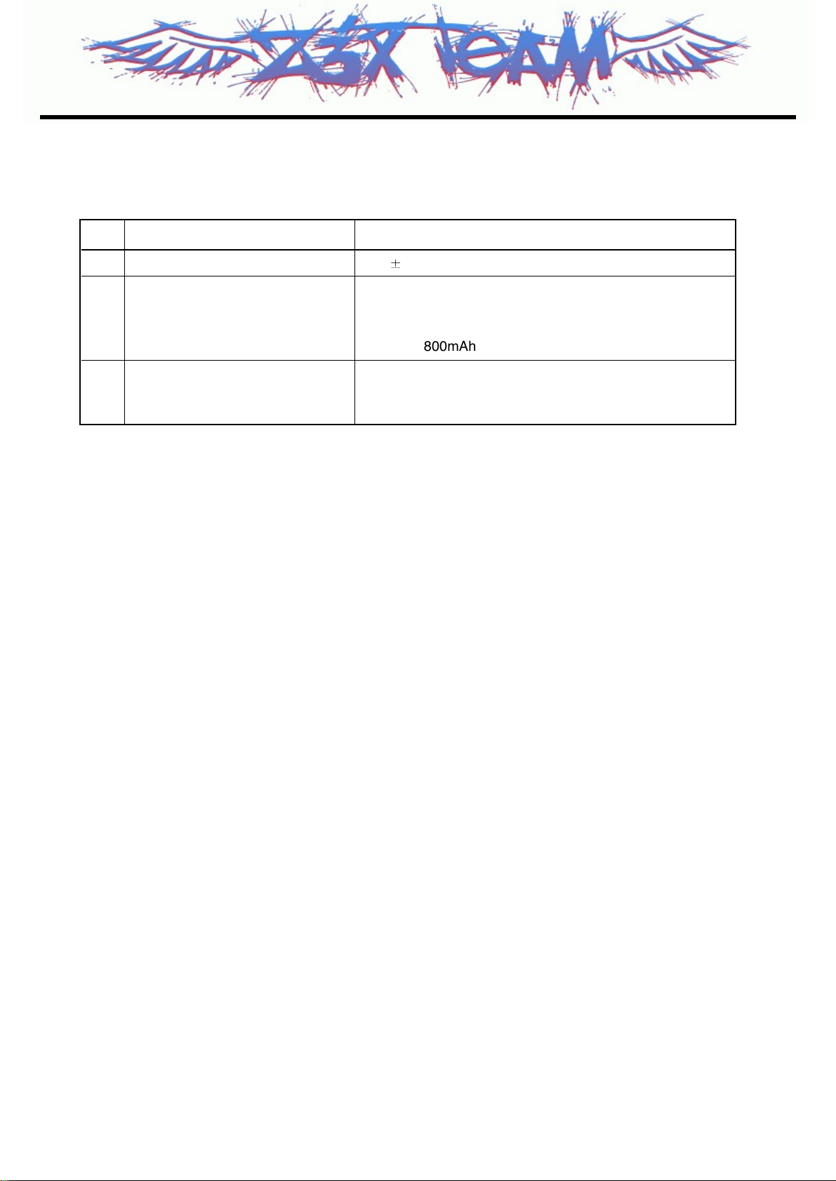
2. PERFORMANCE
- 22 -
Item Description Specification
25 Forced shut down Voltage 3.35 0.03 V
1 Li-ion Battery
26 Battery Type
Standard Voltage = 3.7 V
Battery full charge voltage = 4.2 V
Capacity: 800mAh
Switching-mode charger
27 Travel Charger Input: 100 ~ 240 V, 50/60Hz
Out put: 5.2V, 800mA
Z3X-BOX.COM

3. TECHNICAL BRIEF
- 23 -
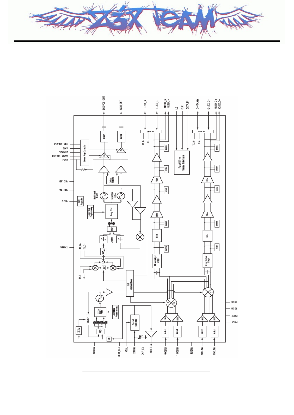
3.1 Power Transceiver (SKY74400, U500)
The RF parts consist of a transmitter part, a receiver part, a frequency synthesizer part, a voltage
supply part, and a VCTCXO part.
The SKY74400 power transceiver is a highly integrated device for quad-band Global System for
Mobile Communications (GSM), General Packet Radio Service (GPRS), and Enhanced Data for GSM
Evolution (EDGE) handsets. The device supports GSM850, EGSM900, DCS1800, and PCS1900
applications.
The power transceiver consists of a direct conversion receiver and power amplifier (PA) with an
integrated PA Control (iPAC) function, fully integrated into a single module. All RF inputs and outputs
of the device are fully matched to 50Ω.
The receiver path implements a direct down-conversion architecture that eliminates the need for
Intermediate Frequency(IF) components. Four integrated Low Noise Amplifiers (LNAs) are internally
matched to 50Ω, which eliminates the need for external matching components. The receiver path also
contains a quadrature demodulator, selectable receiver baseband filter bandwidths, low droop DCoffset correction sequencer, and integrated 2nd order Intercept Point (IP2) calibration circuitry.
The SKY74400 also features an integrated, fully programmable, sigma-delta fractional-N synthesizer
suitable for EGPRS multi-slot operation. The reference frequency for the synthesizer is supplied by an
integrated Voltage Controlled Crystal Oscillator (VCXO) circuit that enables the use of a low-cost
crystal.
The VCXO also provides a buffered output to supply other devices in the system.
The transmit path uses a translation loop architecture. This architecture consists of an In-phase and
Quadrature (I/Q) modulator and a frequency translation loop to perform frequency up-conversion with
high spectral purity. The translation loop also contains a phase-frequency detector, charge pump,
mixer, programmable dividers, and high power transmit Voltage Controlled Oscillators (VCOs) with no
external tank required. The transmit loop is directly connected to the PA section of the power
transceiver, which consists of separate GSM850/EGSM900 and DCS1800/PCS1900 blocks fabricated
on a single GaAs Heterojunction Bipolar Transistor (HBT) die, impedance matching circuitry for 50Ω
output, and a custom BiCMOS PA control block with an internal current-sense resistor.
• Receive section. Includes four integrated LNAs with 50Ω inputs, quadrature demodulator circuitry
that performs direct down-conversion, baseband amplifier circuitry with I/Q outputs, baseband filter
with programmable bandwidths, five stages of DC offset correction, and IP2 calibration circuitry.
• Synthesizer section. Includes an integrated VCO locked by a fractional-N synthesizer loop, a crystal
oscillator to supply the reference frequency, a reference frequency output buffer, and an integrated
loop filter.
• Transmit section. The transmit section is designed with a translation loop architecture that consists of
an I/Q modulator, integrated high power VCOs, offset mixer, programmable divider,
Phase/Frequency Detector (PFD), charge pump, and loop filter. The transmit section also includes a
PA for GSM850/EGSM900 and DCS1800/PCS1900 operation with common power supply pins, 50Ω
output impedance matching circuitry, and a Power Amplifier Controller (PAC) block with an internal
current-sense resistor.
3. TECHNICAL BRIEF
Z3X-BOX.COM
3. TECHNICAL BRIEF
- 24 -
Figure. 3-1 SKY74400 FUNCTIONAL BLOCK DIAGRAM
Z3X-BOX.COM

3. TECHNICAL BRIEF
- 25 -
(1) Receiver Part
A. LNA and Quadrature Demodulator
Four separate LNAs are integrated in the SKY74400 to address different bands of operation. These LNAs have
separate singleended 50Ωinputs. The LNA gain is switchable between high and low settings using the three-wire
bus. The LNA outputs feed into a quadrature demodulator that downconverts the RF signals directly to baseband.
The baseband I and Q paths consist of cascaded amplifiers and low pass filter sections. The baseband section
provides eight programmable bandwidth settings ranging between 90 kHz and 160 kHz to allow for added
flexibility when interfacing to any mixed signal baseband device.
No external capacitors are required for baseband filtering. The filter chain consists of two fixed real poles, two
fixed conjugate pole pairs, and one programmable conjugate pole pair. The result is a flat passband with minimal
group delay distortion at any bandwidth setting.
B. DC Offset Correction
Five DC offset correction loops ensure that DC offsets generated in the SKY74400 do not overload the
baseband chain at any point. After correction, the corrected voltages are held digitally for the duration of the
receive slot(s). The positive edge of the RXENA signal starts the digital DC offset correction. Since the correction
is digital, a system clock is required.
To generate the clock, the reference frequency is divided down internally. A special, fast DC offset correction is
carried out every time the receiver gain is programmed while RXENA is high. This ensures that a DC offset
correction is complete in the time available, even if the gain is changed between slots in multislot mode.
C. AM Suppression and IP2 Calibration
For direct conversion GSM applications, it is imperative to have extremely low second-order distortion.
Mathematically, secondorder distortion of a constant tone generates a DC term proportional to the square of the
amplitude. In general, a strong interfering Amplitude Modulated (AM) signal is, therefore, demodulated by secondorder distortion, which generates an Acinterfering baseband signal. The SKY74400 can effectively handle such
AM-modulated interferers. A commonly used measure for receiver second-order distortion is the second-order
intercept point, IP2. For example, to ensure that the unwanted baseband signals are 9 dB below the wanted signal
required under the AM suppression test for type approval (see 3GPP TS 51.010-1), an input IP2 of 43 dBm is
required. The SKY74400 RF transceiver includes a circuit that minimizes second-order distortion. This IP2
calibration circuit effectively compensates for any second-order distortion in the receive chain that would
otherwise generate unwanted baseband signals in the presence of strong interfering signals. When calibrated
correctly, the SKY74400 IP2 meets the GSM AM suppression test requirements in all bands with good margin.
A one-time factory calibration procedure produces a set of I/Q compensation coefficients that are programmed in
the device to minimize the DC voltage shift resulting from the second-order distortion. The IP2 performance is
optimized when the DC due to the interfering signal is minimized. The determined coefficients are transmitted to
the serial interface, stored in nonvolatile memory, and programmed to the SKY74400 upon each power-up as part
of device initialization. The optimization process is performed internal to the SKY74400.
D. Flexible Receiver Bandwidth Control
The receive baseband filters have programmable bandwidths with eight possible settings.
Z3X-BOX.COM
3. TECHNICAL BRIEF
- 26 -
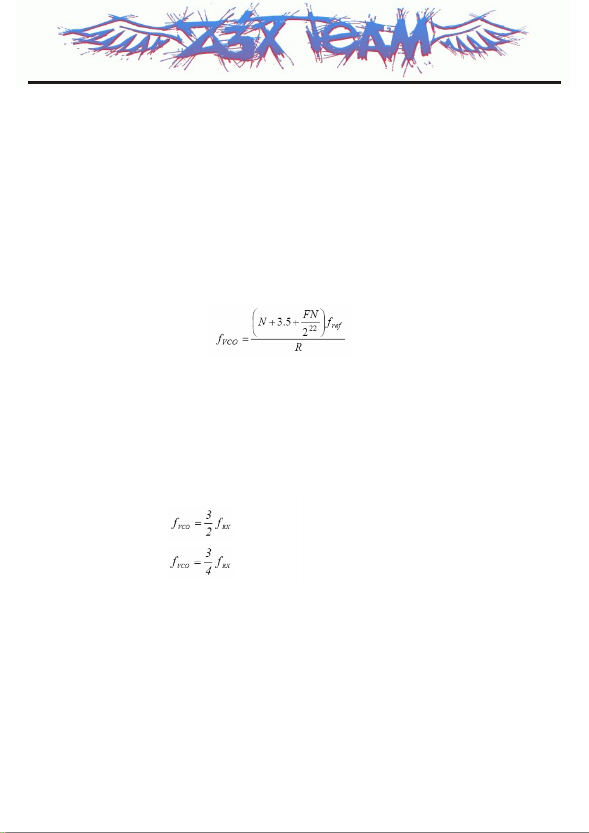
(2) Synthesizer Section
The SKY74400 includes a fully integrated UHF VCO and 3rd order loop filter. A single sigma-delta
fractional-N synthesizer phaselocks the Local Oscillator (LO) used in both transmit and receive paths
to a precision frequency reference input. Fractional-N operation offers low phase noise and fast
settling times, allowing for multiple slot applications such as GPRS.
The SKY74400 frequency stepping function with a 3 Hz resolution allows quad band operation in both
transmit and receive bands using a fully integrated UHF VCO. The fine synthesizer resolution allows
direct compensation or adjustment for reference frequencyerrors.
The generated frequency is given by the following equation:
where: fvco = Generated VCO frequency
N = N-divider ratio, integer part
FN = Fractional setting
R = R-divider ratio
fref = Reference frequency
A. UHF VCO Frequency Setting
To tune the receiver’s receive frequency (fRX), the VCO frequency (fVCO) is set according to the
following equations:
GSM850/EGSM900:
DCS1800/PCS1900:
B. Digital Frequency Centering
The SKY74400 re-centers the UHF VCO frequency range each time the synthesizer is programmed.
This proprietary Skyworks technique, called Digital Frequency Centering (DFC) extends the VCO
frequency coverage, speeds up settling time, and ensures robust performance since the VCO is
always operated at the center of its tuning range. Each time the synthesizer is programmed, the DFC
circuit is activated and the VCO is centered to the programmed frequency in less than 20 µs. After this,
normal Phase Locked Loop (PLL) operation is resumed and the fine settling of the frequency is
finalized. DFC typically adjusts the VCO center frequency to within a few MHz and no more than 5
MHz offset, and presets the tuning voltage to the center of the range before the PLL takes over.
Z3X-BOX.COM

3. TECHNICAL BRIEF
- 27 -
This speeds up frequency settling and ensures that the PLL control voltage never operates close to
the rails. DFC is the result of an adaptive circuit that corrects for any VCO center frequency errors
caused by variations of the integrated VCO circuit such as temperature, supply voltage, or aging. The
VCO can be centered at any frequency in the range from 990 MHz to 1550 MHz. Once centered, the
VCO has a minimum analog tuning range of 20 MHz. No calibration or data storage is needed for DFC
operation. It is activated by one of two events:
• When the synthesizer is programmed, the rising edge of the LE signal starts the DFC cycle
• When the SXENA signal level is changed from low to high, which enables the synthesizer, the rising
edge of the SXENA signal starts the DFC cycle.
C. Integrated Loop Filters
Both loop filters (for the UHF PLL and for the transmit PLL) are fully integrated. Several adjustments
can be made to the loop filter transfer functions. The UHF loop filter has two synchronized charge
pumps. The frequency of the “zero” factor (z1) in the PLL phase transfer function can be adjusted by
varying the charge pump currents, and the values of the internal R3 resistor and C3 capacitor.
Charge Pump Current Compensation for Constant PLL Bandwidth The VCOs in the SKY74400 use
Skyworks DFC technique. The nature of the DFC circuit increases the VCO control sensitivity (KVCO)
as the VCO frequency is increased. Without any compensation, this leads to an increase in the PLL
loop gain and an increased loop bandwidth for higher frequencies. In a classical PLL design, KVCO is
typically regarded as a constant. In this case, the loop gain decreases with increased frequency as the
division ratio of the loop is increased proportionally to frequency. Since it is usually desirable to keep
the loop bandwidth constant over the frequency range of interest, the SKY74400 includes a circuit that
compensates the charge pump current to keep the overall loop gain constant.
Charge pump current compensation for the UHF PLL can be programmed to one of three settings
(nominal, high, or low) or the charge pump current can be programmed to a constant value without
compensation. Refer to the Skyworks Programming Guide SKY74117 RF Transceiver for Standalone
Devices or Embedded MCMs for details.
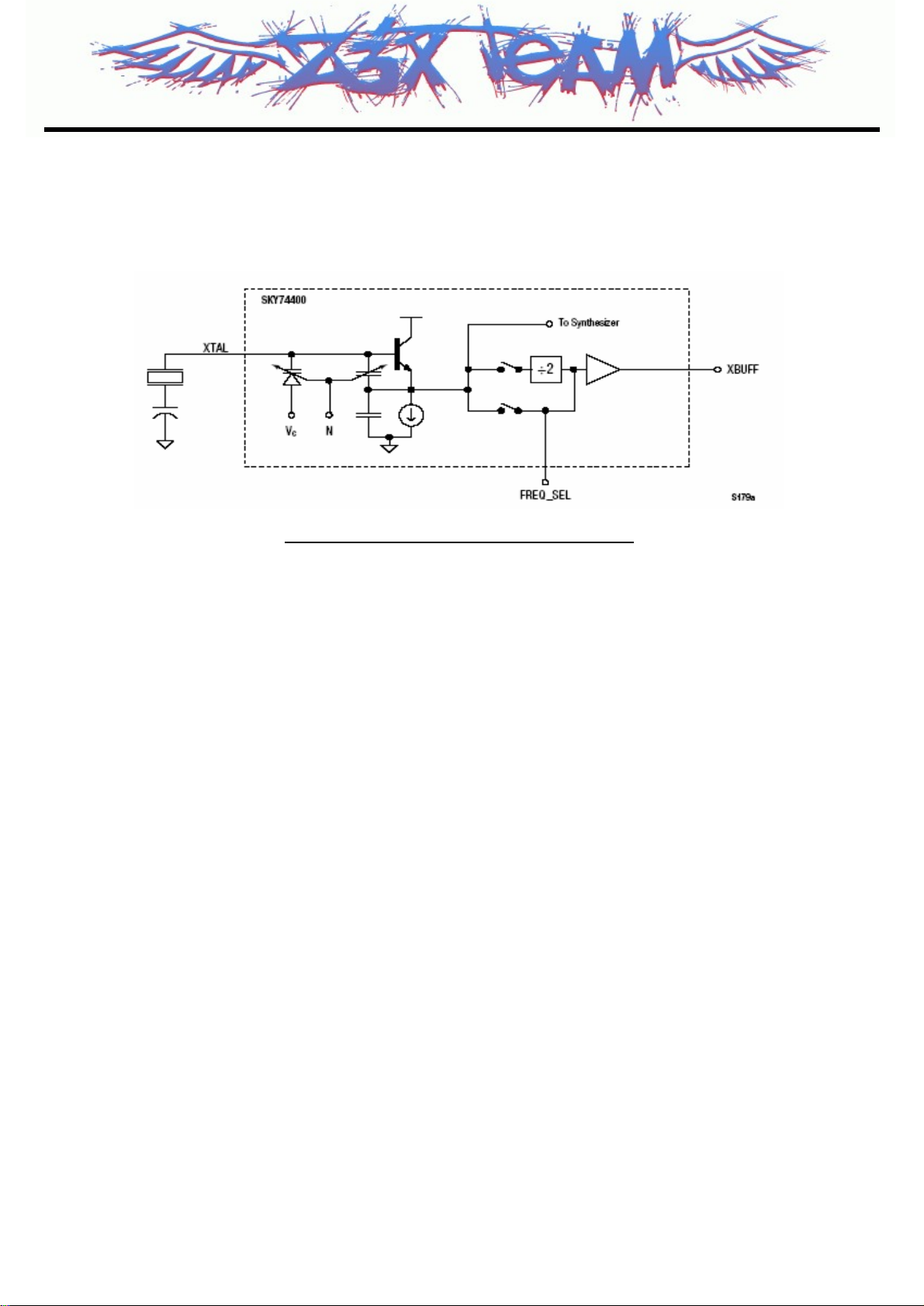
D. Crystal Oscillator
A 26 MHz crystal oscillator provides the reference frequency for the synthesizer. the oscillator uses an
external 26 MHz crystal to generate an accurate oscillation frequency. The reference frequency can be
changed through coarse-tuning with an integrated capacitor array or fine-tuning with the integrated
varactor diode. The oscillator is coarse-tuned by switching in and out (using a digital word
programmed with the serial interface) the capacitor network (CAP_A and CAP_B) located at the input
of the integrated buffer. The oscillator is fine-tuned by providing a tuning voltage to the integrated
varactor diode.
An output buffer is provided to drive the baseband circuitry. The frequency of the output is determined
by the FREQ_SEL signal. When this signal is connected to ground, the output is 13 MHz; when
connected to VCC or left floating, the output is 26 MHz. The oscillator core powers up when the
SXENA signal is set to logic 1.
Z3X-BOX.COM
3. TECHNICAL BRIEF
- 28 -
(3) Transmitter Part
To minimize the post-PA filtering requirements and any additional post-power amp losses, the transmit path
consists of a vector modulator and a frequency translation loop. The translation loop consists of the
following:
• PFD and charge pump
• In-loop modulator
• One programmable divider
• Integrated transmit loop filter
• Two transmit VCOs and output buffers
A. Translation Loop
The translational loop includes a vector modulator and a frequency translation loop to minimize the post-PA
filtering requirements. the loop functions as a PLL with a mixer in the feedback path and a modulator in the
reference path. The loop provides a PFD and charge pump, integrated loop filters, two transmit VCOs,
down-conversion mixer in the feedback path, a frequency divider for frequency plan flexibility, and the
modulator. The mixers in the feedback path provide either high side or low side injection to provide flexibility
in the frequency plan. The modulator in the reference path uses a vector summing technique to reject the
unwanted image and to also sufficiently attenuate the 3rd and 5th harmonics. Therefore, no external IF
filters are required. The loop filter required for the transmit VCOs is integrated in the SKY74400.
B. Transmit VCOs
Two integrated transmit VCOs are designed to meet GSM850, EGSM900, DCS1800, and PCS1900
requirements. The transmit VCOs use the same DFC technique as the synthesizer section to lock the
translation loop. The rising edge on TXENA initializes the transmit DFC. The output buffers feed the signal
to the PAs. Two transmit buffers are provided, one for the low band VCO and the other for the high band
VCO.
Figure. 3-2 Crystal Oscillator BLOCK DIAGRAM
Z3X-BOX.COM

3. TECHNICAL BRIEF
- 29 -
C. Power Amplifier (PA)
The PA functionality of the SKY74400 consists of separate GSM850/EGSM900 and DCS1800/PCS1900
blocks, impedancematching circuitry for 50Ωoutput impedances, and a PAC block with an internal
currentsense resistor. The custom BiCMOS integrated circuit provides the internal PAC function and
interface circuitry. Fabricated onto a single Gallium Arsenide (GaAs) die, one Heterojunction Bipolar
Transistor (HBT) PA block supports the GSM850 and EGSM900 bands, and the other supports the
DCS1800 and PCS1900 bands. Both PA blocks share common power supply pins to distribute current. The
RF output ports of the SKY74400 are internally matched to a 50 load to reduce the number of external
components for a quad-band design. The PA also contains band-select switching circuitry to select GSM
(logic 0) or DCS/PCS (logic 1) as determined from the BAND_SELECT signal. The VBAT pin connects to an
internal current-sense resistor and interfaces to an iPAC function, which is insensitive to variations in
temperature, power supply, and process.
The ENABLE input allows initial power-on of PA circuitry to minimize battery drain.
(4) Low Drop-Out (LDO) Linear Voltage Regulators
The SKY74400 includes integrated LDO linear voltage regulators to eliminate the need for a separate power
management integrated circuit or discrete voltage regulators. Each functional block in the SKY74400
includes a separate, internal LDO voltage regulator.
Z3X-BOX.COM
3. TECHNICAL BRIEF
- 30 -
3.2 13 MHz Clock (VCTCXO, X500)
The 13 MHz clock(X500) consists of a TCXO(Temperature Compensated Crystal Oscillator) which
oscillates at a frequency of 13 MHz. It is used within the SKY74400, analog base band chipset (U101,
AD6535), digital base band chipset (U102, AD6527B).
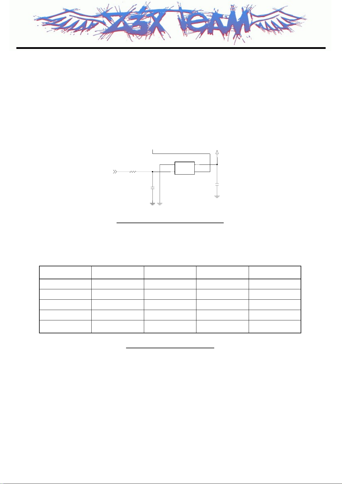
3.3 Switchplexer for Triband(FL500)
Figure 3-3 VCTCXO CIRCUIT DIAGRAM
Vc1 Vc2 Vc3 Current
GSM850 -Tx 0.0-0.1V 0.0-0.1V 2.3-3.0V 10mA Max
GSM850 -Rx 0.0-0.1V 0.0-0.1V 0.0-0.1V ≈ 0mA
DCS/PCS-Tx 0.0-0.1V 2.3-3.0V 0.0-0.1V 10mA Max
DCS-Rx 0.0-0.1V 0.0-0.1V 0.0-0.1V ≈ 0mA
PCS-Rx 2.3-3.0V 0.0-0.1V 0.0-0.1V 10mA Max
Table 3-1 FEM CONTROL LOGIC
2V75_VVCXO
1M
13MHz
GND
VCC
AFC
R505
10K
C530
1000p
2
1
VCONT
X500
OUT
4
3
C529
(1005)
1u
Z3X-BOX.COM
3. TECHNICAL BRIEF
- 31 -
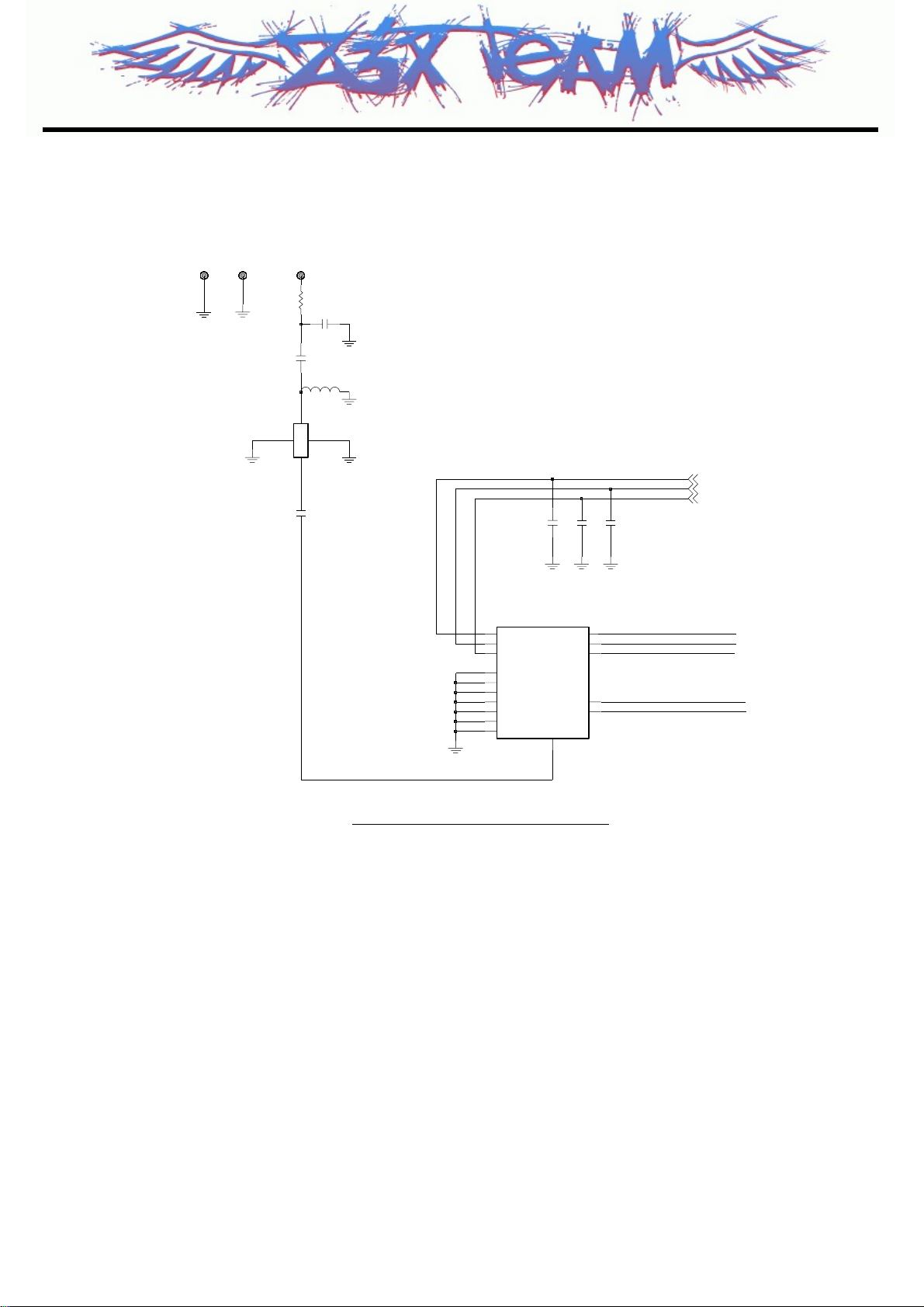
Figure 3-4 FEM CIRCUIT DIAGRAM
TP501
ANT
G1
G2
RF
KMS-506
SW500
NA
L500
C500
ANT
8.2nH
C503 27p
0
C531
1.8p
R500
7
GND4
GND5
14
15
GND6
GND7
16
GSM18001900_TX
8
GSM1800_RX
4
GSM1900_RX
6
GSM900_RX
2
10
GSM900_TX
VC1
11
9
VC2
VC3
12
LMSP54LA-445TEMP
FL500
13
ANT
1
GND1
GND2
3
5
GND3
C505 27p
27pC504
C502
1000p
TP500
ANT_SW2
ANT_SW3
ANT_SW1
Z3X-BOX.COM
 Loading...