

LG MG 280 Diagram

Service Manual
Model : MG280
Service Manual
MG280
Date: February, 2007 / Issue 1.0
Presione tecla Cáma
4:11 am 05/01 Vie

- 3 -
1. INTRODUCTION ...............................5
1.1 Purpose .................................................. 5
1.2 Regulatory Information............................ 5
1.3 Abbreviations .......................................... 7
2. PERFORMANCE...............................9
2.1 H/W Features...........................................9
2.2 Technical Specification ..........................10
3. TECHNICAL BRIEF ........................15
3.1 Power Amplifier (SKY77318, U600).......15
3.2 Transceiver (AD6549, U601) .................17
3.3 FEM for Triband(FL600) ........................19
3.4 26 MHz Clock (VCTCXO, X500)............20
3.5 Baseband Processor (AD6720 , U101)..21
3.6 Battery Charging Block ..........................26
3.7 Display and Interface .............................28
3.8 Camera IC(AIT701G , U401) .................30
3.9 Keypad Switches and Scanning ............32
3.10 Microphone ..........................................34
3.11 Main Speaker.......................................34
3.12 Headset Interface.................................36
3.13 Key Back-light Illumination...................37
3.14 LCD Back-light Illumination..................38
3.15 VIBRATOR...........................................39
3.16 Bluetooth..............................................40
4. TROUBLE SHOOTING ...................41
4.1 RF Component.......................................41
4.2 RX Trouble.............................................42
4.3 TX Trouble .............................................47
4.4 Power On Trouble..................................53
4.5 Charging Trouble ...................................55
4.6 Vibrator Trouble .....................................57
4.7 LCD Trouble...........................................59
4.8 Camera Trouble .....................................62
4.9 Speaker Trouble ....................................65
4.10 SIM Card Interface Trouble..................67
4.11 Earphone Trouble ................................69
4.12 KEY backlight Trouble .........................71
4.13 Receiver Trouble..................................73
4.14 Microphone Trouble .............................75
4.15 RTC Trouble ........................................77
4.16 Slide on/off Trouble..............................79
5. DOWNLOAD.......................................81
5.1 Download ...............................................81
6. BLOCK DIAGRAM ..........................87
7. Circuit Diagram ..............................89
8. pcb layout .......................................99
9. ENGINEERING MODE ..................105
9.1 BB Test [MENU 1]................................106
9.2 RF Test [MENU 2]................................108
9.3 MF mode [MENU 3] .............................108
9.4 Trace option [MENU 4] ........................109
9.5 Call timer [MENU 5] .............................109
9.6 Fact. Reset [MENU 6] ..........................109
9.7 S/W version..........................................109
10. STAND ALONE TEST .................110
10.1 Introduction ........................................110
10.2 Setting Method...................................110
10.3 Means of Test ....................................111
11. AUTO CALIBRATION..................113
11.1 Overview ............................................113
11.2 Equipment List ...................................113
11.3 Test Jig Operation..............................114
11.4 Procedure ..........................................115
11.5 AGC ...................................................118
11.6 APC....................................................118
11.7 ADC ...................................................118
12. EXPLODED VIEW &
REPLACEMENT PART LIST ..... 119
12.1 Exploded View .................................. 119
12.2 Replacement Parts ............................121
12.3 Accessory ......................................... 137
Table Of Contents

- 4 -

1. INTRODUCTION
- 5 -
1.1 Purpose
This manual provides the information necessary to repair, calibration, description and download the
features of this model.
1.2 Regulatory Information
A. Security
Toll fraud, the unauthorized use of telecommunications system by an unauthorized part (for example,
persons other than your company’s employees, agents, subcontractors, or person working on your
company’s behalf) can result in substantial additional charges for your telecommunications services.
System users are responsible for the security of own system. There are may be risks of toll fraud
associated with your telecommunications system. System users are responsible for programming and
configuring the equipment to prevent unauthorized use. The manufacturer does not warrant that this
product is immune from the above case but will prevent unauthorized use of common-carrier
telecommunication service of facilities accessed through or connected to it.
The manufacturer will not be responsible for any charges that result from such unauthorized use.
B. Incidence of Harm
If a telephone company determines that the equipment provided to customer is faulty and possibly
causing harm or interruption in service to the telephone network, it should disconnect telephone
service until repair can be done. A telephone company may temporarily disconnect service as long as
repair is not done.
C. Changes in Service
A local telephone company may make changes in its communications facilities or procedure. If these
changes could reasonably be expected to affect the use of the this phone or compatibility with the
network, the telephone company is required to give advanced written notice to the user, allowing the
user to take appropriate steps to maintain telephone service.
D. Maintenance Limitations
Maintenance limitations on this model must be performed only by the manufacturer or its authorized
agent. The user may not make any changes and/or repairs expect as specifically noted in this manual.
Therefore, note that unauthorized alternations or repair may affect the regulatory status of the system
and may void any remaining warranty.
1. INTRODUCTION

1. INTRODUCTION
- 6 -
E. Notice of Radiated Emissions
This model complies with rules regarding radiation and radio frequency emission as defined by local
regulatory agencies. In accordance with these agencies, you may be required to provide information
such as the following to the end user.
F. Pictures
The pictures in this manual are for illustrative purposes only; your actual hardware may look slightly
different.
G. Interference and Attenuation
Phone may interfere with sensitive laboratory equipment, medical equipment, etc.Interference from
unsuppressed engines or electric motors may cause problems.
H. Electrostatic Sensitive Devices
ATTENTION
Boards, which contain Electrostatic Sensitive Device (ESD), are indicated by the sign.
Following information is ESD handling:
• Service personnel should ground themselves by using a wrist strap when exchange system boards.
• When repairs are made to a system board, they should spread the floor with anti-static mat which is
also grounded.
• Use a suitable, grounded soldering iron.
• Keep sensitive parts in these protective packages until these are used.
• When returning system boards or parts like EEPROM to the factory, use the protective package as
described.

1. INTRODUCTION
- 7 -
1.3 Abbreviations
For the purposes of this manual, following abbreviations apply:
APC Automatic Power Control
BB Baseband
BER Bit Error Ratio
CC-CV Constant Current - Constant Voltage
DAC Digital to Analog Converter
DCS Digital Communication System
dBm dB relative to 1 milli watt
DSP Digital Signal Processing
EEPROM Electrical Erasable Programmable Read-Only Memory
ESD Electrostatic Discharge
FPCB Flexible Printed Circuit Board
GMSK Gaussian Minimum Shift Keying
GPIB General Purpose Interface Bus
GSM Global System for Mobile Communications
IPUI International Portable User Identity
IF Intermediate Frequency
LCD Liquid Crystal Display
LDO Low Drop Output
LED Light Emitting Diode
OPLL Offset Phase Locked Loop

1. INTRODUCTION
- 8 -
PAM Power Amplifier Module
PCB Printed Circuit Board
PGA Programmable Gain Amplifier
PLL Phase Locked Loop
PSTN Public Switched Telephone Network
RF Radio Frequency
RLR Receiving Loudness Rating
RMS Root Mean Square
RTC Real Time Clock
SAW Surface Acoustic Wave
SIM Subscriber Identity Module
SLR Sending Loudness Rating
SRAM Static Random Access Memory
PSRAM Pseudo SRAM
STMR Side Tone Masking Rating
TA Travel Adapter
TDD Time Division Duplex
TDMA Time Division Multiple Access
UART Universal Asynchronous Receiver/Transmitter
VCO Voltage Controlled Oscillator
VCTCXO Voltage Control Temperature Compensated Crystal Oscillator
WAP Wireless Application Protocol
2. PERFORMANCE
- 9 -
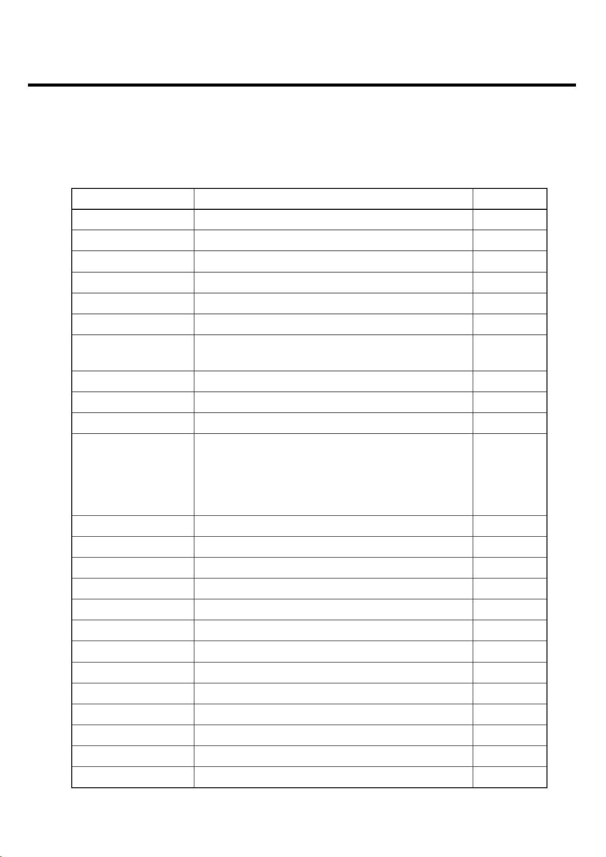
2.1 H/W Features
2. PERFORMANCE
Item Feature Comment
Standard Battery Li-ion Polymer, 3.7V 800mAh
Stand by TIME Up to 200 hrs : Paging Period 5, RSSI 85dBm
Talk time Up to 200min : GSM Tx Level 7
Stand by time Up to 200 hours (Paging Period: 5, RSSI: -85 dBm)
Charging time Approx. 3 hours
RX Sensitivity GSM, EGSM: -109dBm, DCS: -109dBm
TX output power
GSM, EGSM: 32.5dBm(Level 5),
DCS , PCS: 29.5dBm(Level 0)
GPRS compatibility Class 10
SIM card type 3V Small
Display LCD : TFT 128 × 160 pixel 262K Color
Hard icons. Key Pad
0 ~ 9, #, *, Touch Key(Up/Down Navigation Key
Status Indicator Menu Key, Clear Key, Back Key, Confirm Key
Send Key, Soft Key(Left/Right))
Volume Key, PWR Key, Camera Key
ANT Internal
EAR Phone Jack Yes (mono)
PC Synchronization Yes
Speech coding EFR/FR/HR
Data and Fax Yes
Vibrator Yes
Loud Speaker Yes
Voice Recoding Yes
Microphone Yes
Speaker/Receiver One way speaker
Travel Adapter Yes
MIDI 64 Poly (Mono SPK)
Camera VGA
2. PERFORMANCE
- 10 -
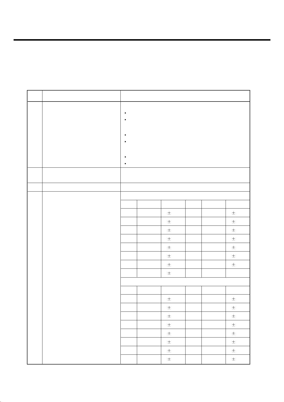
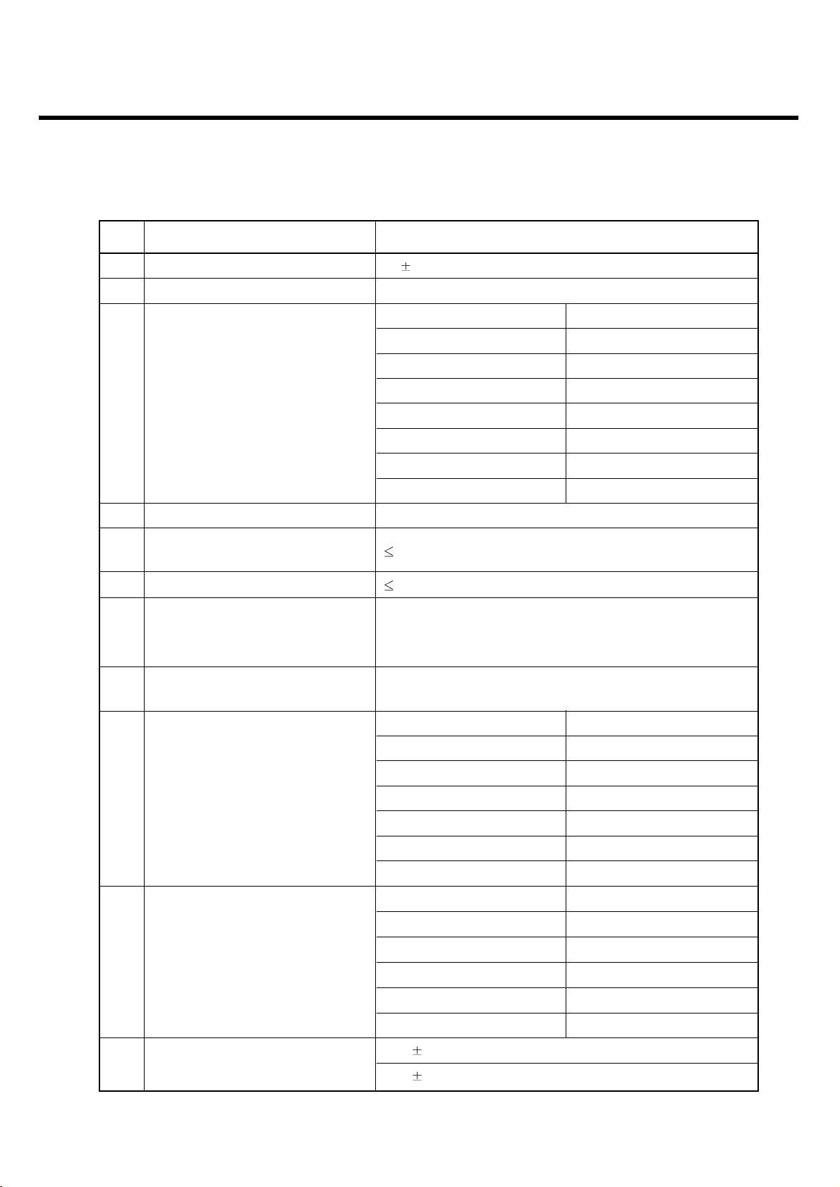
2.2 Technical Specification
Item Description Specification
GSM850
TX: 890 + n x 0.2 MHz
RX: 935 + n x 0.2 MHz (n=1~124)
PCS
1Frequency Band TX: 1850 + (n-512) x 0.2 MHz
RX: 1930+ (n-1512) x 0.2 MHz (n=512~810)
DCS
TX: 1710 + (n-512) x 0.2 MHz
RX: 1805 + (n-512) x 0.2 MHz (n=512~885)
2 Phase Error
RMS < 5 degrees
Peak < 20 degrees
3 Frequency Error < 0.1 ppm
GSM
Level Power Toler. Level Power Toler.
5 33 dBm 2dB 13 17 dBm 3dB
6 31 dBm 3dB 14 15 dBm 3dB
7 29 dBm 3dB 15 13 dBm 3dB
8 27 dBm 3dB 16 11 dBm 5dB
9 25 dBm 3dB 17 9 dBm 5dB
10 23 dBm 3dB 18 7 dBm 5dB
11 21 dBm 3dB 19 5 dBm 5dB
4 Power Level 12 19 dBm 3dB
DCS/PCS
Level Power Toler. Level Power Toler.
0 30 dBm 2dB 8 14 dBm 3dB
1 28 dBm 3dB 9 12 dBm 4dB
2 26 dBm 3dB 10 10 dBm 4dB
3 24 dBm 3dB 11 8 dBm 4dB
4 22 dBm 3dB 12 6 dBm 4dB
5 20 dBm 3dB 13 4 dBm 4dB
6 18 dBm 3dB 14 2 dBm 5dB
7 16 dBm 3dB 15 0 dBm 5dB
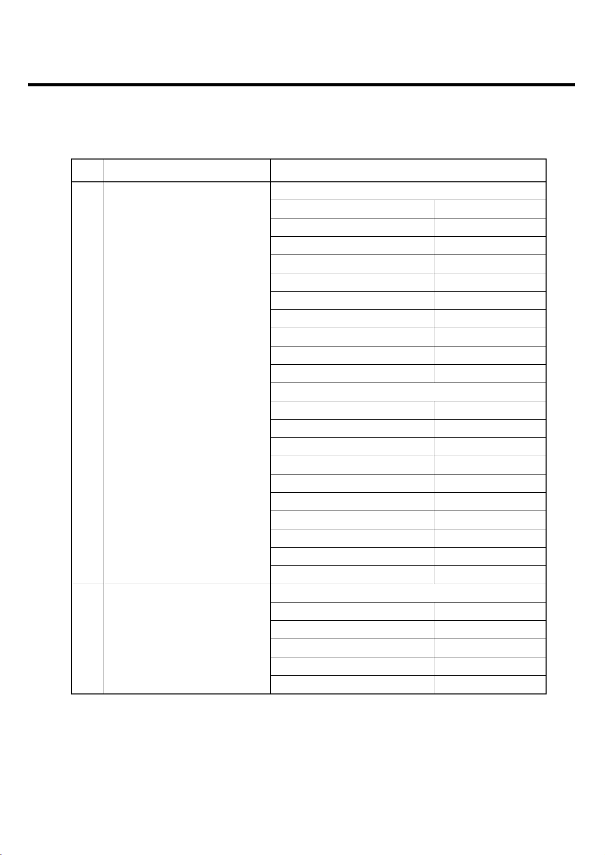
2. PERFORMANCE
- 11 -
Item Description Specification
GSM, EGSM
Offset from Carrier (kHz). Max. dBc
100 +0.5
200 -30
250 -33
400 -60
600~ <1,200 -60
1,200~ <1,800 -60
1,800~ <3,000 -63
3,000~ <6,000 -65
5
Output RF Spectrum 6,000 -71
(due to modulation) DCS/PCS
Offset from Carrier (kHz). Max. dBc
100 +0.5
200 -30
250 -33
400 -60
600~ <1,200 -60
1,200~ <1,800 -60
1,800~ <3,000 -65
3,000~ <6,000 -65
6,000 -73
GSM, EGSM
Offset from Carrier (kHz) Max. (dBm)
Output RF Spectrum 400 -19
6
(due to switching transient) 600 -21
1,200 -21
1,800 -24
2. PERFORMANCE
- 12 -
Item Description Specification
DCS/PCS
Offset from Carrier (kHz). Max. (dBm)
Output RF Spectrum 400 -22
6
(due to switching transient) 600 -24
1,200 -24
1,800 -27
7 Spurious Emissions Conduction, Emission Status
GSM, EGSM
8Bit Error Ratio
BER (Class II) < 2.439% @-102 dBm
DCS,PCS
BER (Class II) < 2.439% @-100 dBm
9 RX Level Report Accuracy 3 dB
10 SLR 8 3 dB
Frequency (Hz) Max.(dB) Min.(dB)
100 -12 -
200 0 -
300 0 -12
11 Sending Response 1,000 0 -6
2,000 4 -6
3,000 4 -6
3,400 4 -9
4,000 0 -
12 RLR 2 3 dB
Frequency (Hz) Max.(dB) Min.(dB)
100 -12 -
200 0 -
300 2 -7
500
*
-5
13 Receiving Response 1,000 0 -5
3,000 2 -5
3,400 2 -10
4,000 2
*
Mean that Adopt a straight line in between 300 Hz
and 1,000 Hz to be Max. level in the range.
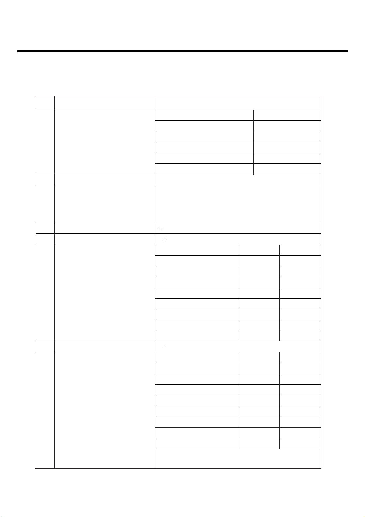
2. PERFORMANCE
- 13 -
Item Description Specification
14 STMR 13 5 dB
15 Stability Margin > 6 dB
dB to ARL (dB) Level Ratio (dB)
-35 17.5
-30 22.5
-20 30.7
16 Distortion
-10 33.3
0 33.7
7 31.7
10 25.5
17 Side Tone Distortion Three stage distortion < 10%
18
System frequency
2.5ppm
(13 MHz) tolerance
19 32.768KHz tolerance 30ppm
At least 65 dBspl under below conditions:
20 Ringer Volume 1. Ringer set as ringer.
2. Test distance set as 50 cm
21 Charge Current
Fast Charge : < 430 mA
Slow Charge : < 160 mA
Antenna Bar Number Power
5 -85 dBm ~
4-90 dBm ~ -86 dBm
22 Antenna Display 3 -95 dBm ~ -91 dBm
2-100 dBm ~ -96 dBm
1-105 dBm ~ -101 dBm
0~ -105 dBm
Battery Bar Number Voltage
0 3.48 ~ 3.63 V
23 Battery Indicator 1 3.63 ~ 3.70 V
2 3.70 ~ 3.76 V
3 3.76 ~ 3.89 V
43.89 V ~
24 Low Voltage Warning
3.63 0.03V (Call) every 1 minutes
3.48 0.03V (Standby)
2. PERFORMANCE
- 14 -
Item Description Specification
25 Forced shut down Voltage 3.33 0.03 V
1 Li-ion Battery
26 Battery Type
Standard Voltage = 3.7 V
Battery full charge voltage = 4.2 V
Capacity: 830mAh
Switching-mode charger
27 Travel Charger Input: 100 ~ 240 V, 50/60 Hz
Output: 5.2 V, 800 mA
3. TECHNICAL BRIEF
- 15 -
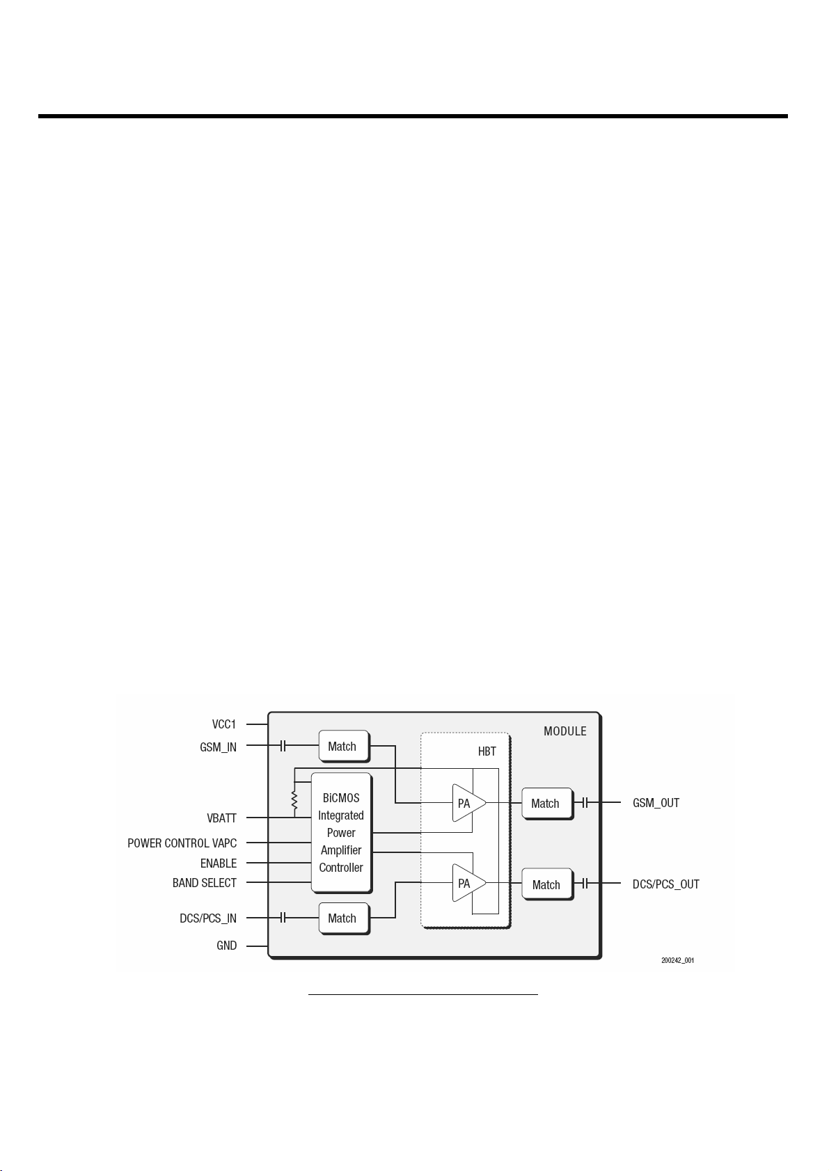
3.1 Power Amplifier (SKY77318, U600)
The SKY77318 Power Amplifier Module (PAM) is designed in a low profile (1.2 mm), compact form
factor for quad-band cellular handsets comprising GSM850/900, DCS1800, and PCS1900 operation.
The PAM also supports Class 12 General Packet Radio Service (GPRS) multi-slot operation. The
module consists of separate GSM850/900 PA and DCS1800/PCS1900 PA blocks,
impedancematching circuitry for 50 Ω input and output impedances, and a Power Amplifier Control
(PAC) block with an internal current-sense resistor. The custom BiCMOS integrated circuit provides
the internal PAC function and interface circuitry. Fabricated onto a single Gallium Arsenide (GaAs) die,
one Heterojunction Bipolar Transistor (HBT) PA block supports the GSM850/900 bands and the other
supports the DCS1800 and PCS1900 bands. Both PA blocks share common power supply pins to
distribute current. The GaAs die, the Silicon (Si) die, and the passive components are mounted on a
multi-layer laminate substrate. The assembly is encapsulated with plastic overmold. RF input and
output ports of the SKY77318 are internally matched to a 50 Ω load to reduce the number of external
components for a quad-band design. Extremely low leakage current (2.5 µA, typical) of the dual PA
module maximizes handset standby time. The SKY77318 also contains band-select switching circuitry
to select GSM (logic 0) or DCS/PCS (logic 1) as determined from the Band Select (BS) signal. In
Figure 1 below, the BS pin selects the PA output (DCS/PCS OUT or GSM850/900 OUT) and the
Analog Power Control (VAPC) controls the level of output power. The VBATT pin connects to an
internal current-sense resistor and interfaces to an integrated power amplifier control (iPAC™)
function, which is insensitive to variations in temperature, power supply, process, and input power.
The ENABLE input allows initial turn-on of PAM circuitry to minimize battery drain. Figure 1.
Functional Block Diagram
3. TECHNICAL BRIEF
Figure1. Functional Block Diagram
3. TECHNICAL BRIEF
- 16 -
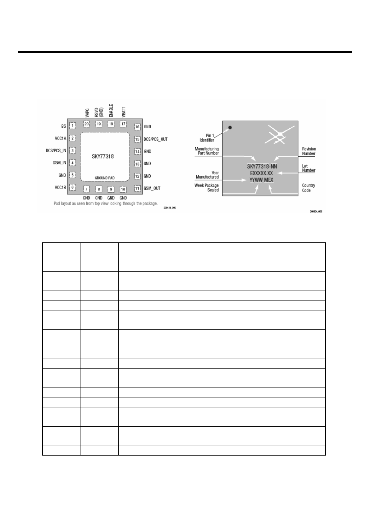
SKY77318 PAM Pin Configuration-20-Pin
Leadless (Top View)
Figure 6. Typical Case Makings
Table 4. SKY77328 Pin Names and Signal Descriptions
Pin Mame Description
1BSBand Select
2 VCC1A VCC (to GSM 1st stage, DCS/PCS 1st stages, BiCMOS PAC)
3 DCS/PCS IN RF input 1710-1910 MHz (DCS1800, PCS1900)
4 GND IN RF input 880-915 MHz (GSM)
5 GND RF and DC Ground
6 VCC1B VCC (to GSM 2nd stage, DCS/PCS 2nd stages)
7 GND RF and DC Ground
8 GND RF and DC Ground
9 GND RF and DC Ground
10 GND RF and DC Ground
11 GSM OUT RF Output 880-915 MHz (GSM)
12 GND RF and DC Ground
13 GND RF and DC Ground
14 GND RF and DC Ground
15 DCS/PCS OUT RF Output 1710-1910 MHz (DCS 1800, PCS1900)
16 GND RF and DC Ground
17 VBATT Battery input to high side of intemal sense resistor
18 ENABLE BiCMOS Enable
19 RSVD(GND) RF and DC Ground
20 VAPC Power Control Bias Voltage
GMD PAD GND Ground Pad, device underside
3. TECHNICAL BRIEF
- 17 -
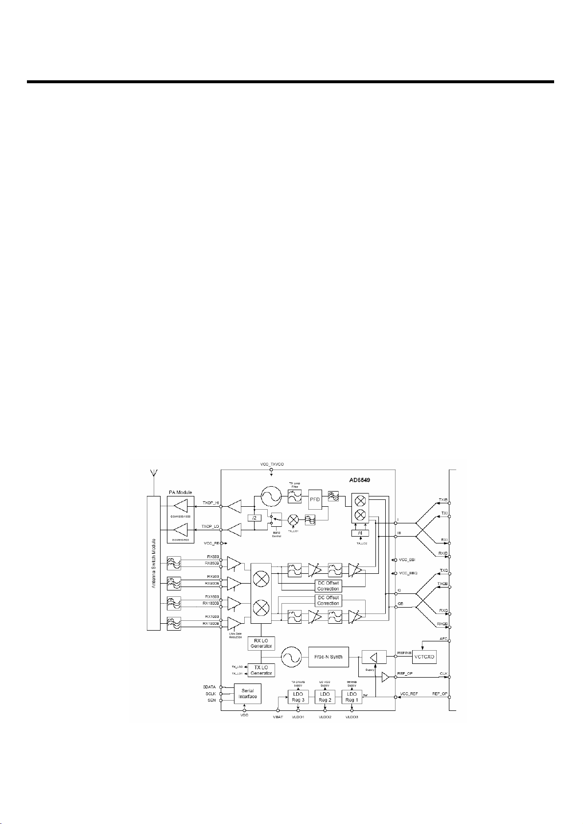
3.2 Transceiver (AD6549, U601)
The AD6548/9 provides a highly integrated direct conversion radio solution that combines, on a single chip, all
radio and power management functions necessary to build the most com-pact GSM radio solution possible. The
only external components required for a complete radio design are the Rx SAWs, PA, Switchplexer and a few
passives enabling an extremely small cost effective GSM Radio solution. The AD6548/9 uses the industry proven
direct conversion re-ceiver architecture of the OthelloTM family. For Quad band appli-cations the front end
features four fully integrated programmable gain differential LNAs. The RF is then downconverted by quad-rature
mixers and then fed to the baseband programmable-gain amplifiers and active filters for channel selection. The
Receiver output pins can be directly connected to the baseband analog processor. The Receive path features
automatic calibration and tracking to remove DC offsets. The transmitter features a translation-loop architecture
for di-rectly modulating baseband signals onto the integrated TX VCO. The translation-loop modulator and TX
VCO are extremely low noise removing the need for external SAW filters prior to the PA. The AD6548/9 uses a
single integrated LO VCO for both the receive and the transmit circuits. The synthesizer lock times are optimized
for GPRS applications up to and including class 12. AD6548 incorporates a complete reference crystal calibration
system. This allows the external VCTCXO to be replaced with a low cost crystal. No other external components
are required. The AD6549 uses the traditional VCTCXO reference source. The AD6548/9 also contains on-chip
low dropout voltage regula-tors (LDOs) to deliver regulated supply voltages to the functions on chip, with a battery
input voltage of between 2.9V and 5.5V. Comprehensive power down options are included to minimize power
consumption in normal use. A standard 3 wire serial interface is used to program the IC. The interface features
low-voltage digital interface buffers compatible with logic levels from 1.6V to 2.9V.
Figure 2 AD6549 Block Diagram
3. TECHNICAL BRIEF
- 18 -
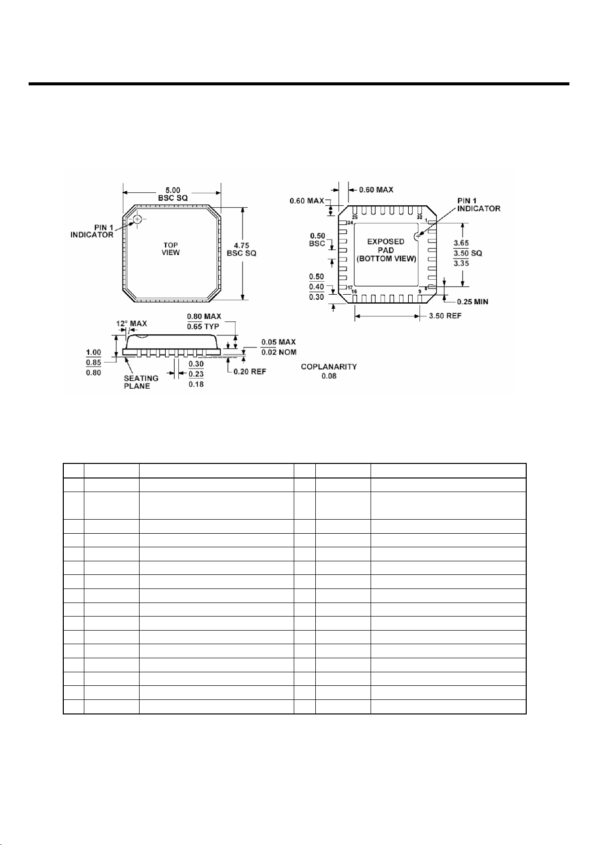
Table 1 AD6548/9 Pin Descriptions
No Name Description No Name Description
1 VCC_FE Front end supply (IP) 17 VCC_REF Reference Oscillator Supply (IP)
2I I baseband input/output 18 VAFC/ AD6548 Crystal Freq control (IP)
N/C AD6549: Spare Pin
3IBI baseband input/output 19 REFIN Crystal Connection
4 VCC_BBI Baseband I, TX path supply (IP) 20 REFINB Crystal Connection
5 SDATA Serial port data 21 REF_OP Reference Frequency Output
6 SCLK Serial port clock 22 QB Q baseband input/output
7 SEN Serial port enable 23 Q Q baseband input/output
8 N/C Not connected 24 VCC_BBQ Baseband Q supply (IP)
9 VLDO3 TX LDO Output (1) 25 RX1900B PCS 1900 LNA input
10 TXOP_LO Transmit O/P (850/900MHz) 26 RX1900 PCS 1900 LNA input
11 TXOP_HI Transmit O/P (1800/1900MHz) 27 RX1800B DCS 1800 LNA input
12 VCC_TXVCO TX VCO supply (1) 28 RX1800 DCS 1800 LNA input
13 VDD Serial interface supply 29 RX900B E-GSM LNA input
14 VBAT Battery I/P for LDO reg’s 30 RX900 E-GSM LNA input
15 VLDO1 LDO regulator Output (2) 31 RX850B GSM 850 LNA input
16 VLDO2 LO VCO Supply (3) 32 RX850 GSM 850 LNA input
GOMPLIANT TO JEDEC STANDARDS MO-220-VHHD-2
3. TECHNICAL BRIEF
- 19 -
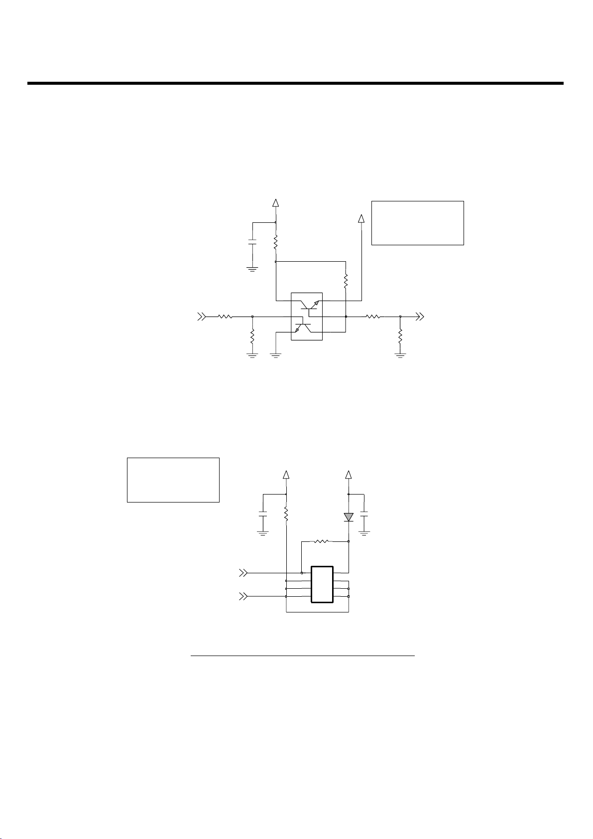
3.3 FEM for Triband(FL600)
Table 3-1 Band SW Logic Table
Figure 3- 2 FEM CIRCUIT DIAGRAM
R617 100ohm
GND6
19
GND7
20
10
GSM1800_1900_TX
5
GSM1800_RX_OUT1
6
GSM1800_RX_OUT2
GSM1900_RX_OUT1
7
8
GSM1900_RX_OUT2
GSM850_900_TX
12
GSM850_RX_OUT1
1
2
GSM850_RX_OUT2
GSM900_RX_OUT1
3
GSM900_RX_OUT2
4
VC1
14
VC2
15
LSHS-M085FJFL600
17
ANT
GND1
9
GND2
11
13
GND3
GND4
16
18
GND5
C630
39p
39p
C631
100ohmR616
22p
C615
ANT_SW2
ANT_SW1
ANT_SW1 ANT_SW2
GSM_TX High Low
DCS/PCS_TX Low High
GSM_RX Low Low
DCS_RX Low Low
PCS_RX Low Low
3. TECHNICAL BRIEF
- 20 -
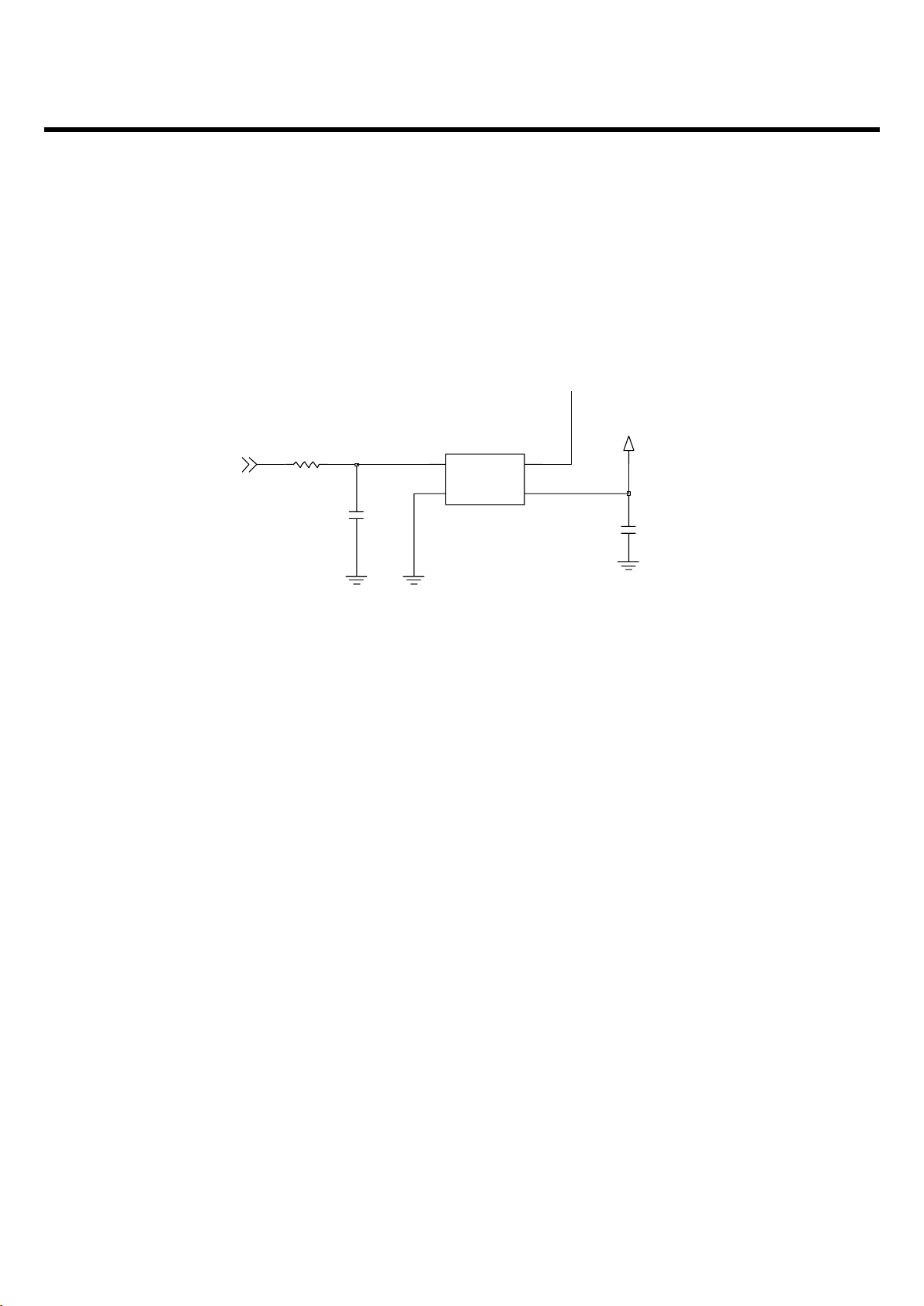
3.4 26 MHz Clock (VCTCXO, X500)
The 26 MHz clock(X600) consists of a TCXO(Temperature Compensated Crystal Oscillator) which
oscillates at a frequency of 26 MHz. It is used within the SKY77318, base band
processor(AD6720,U101), Midi(U204, YMU792) , CAMERA( U401,AIT701G )
Figure 3-3. VCTCXO CIRCUIT DIAGRAM
2V75_VVCXO
X600
1
2
VCONT
GND
OUT
VCC
3
4
26MHz
TG-5010LH-26M
EXSK0008101
C648
2.2u
AFC
R622
15K
C647
1000p

3. TECHNICAL BRIEF
- 21 -
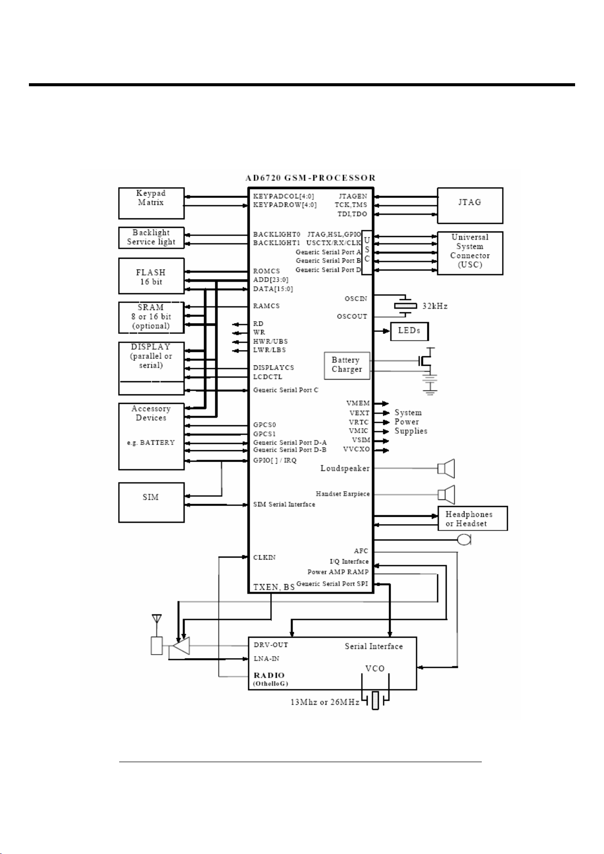
3.5 Baseband Processor (AD6720 , U101)
• AD6720 is an ADI designed processor
• AD6720 consists of
1. Control Processor Subsystem including:
• 32-bit MCU ARM7TDMI® Control Processor
• 39 MHz operation at 1.8V
• 1Mb of on-chip System SRAM Memory
2. DSP Subsystem including:
• 16-bit Fixed Point DSP Processor
• 91 MIPS[1] at 1.8V
• Data and Program SRAM
• Program Instruction Cache
• Full Rate, Enhanced Full Rate and Half Rate
• Speech Encoding/Decoding
• Capable of Supporting AMR & PDC Speech Algorithms
3. Peripheral Functions
• Parallel and Serial Display Interface
• Keypad Interface
• Flash Memory Interface
• Page-Mode Flash Support
• 1.8V and 3.0V, 64 kbps SIM Interface
• Universal System Connector Interface
• Data Services Interface
• Battery Interface (e.g. Dallas)
4. Other
• Supports 13 MHz and 26 MHz Input Clocks
• 1.8V Typical Core Operating Voltages
• 289-Ball Package (12x12mm), 0.65mm Ball pitch
5. The AD6720 baseband transmit section supports the following mobile station GMSK modulation
power classes:
• GSM 900/850 power classes 4 and 5,
• DCS 1800 power classes 1 and 2, and
• PCS 1900 power classes 1 and 2
3. TECHNICAL BRIEF
- 22 -
Figure 3-4 SYSTEM INTERCONECTION OF AD6720 EXTERNAL INTERFACE
3. TECHNICAL BRIEF
- 23 -
3.5.1 Interconnection with external devices
A. RTC block interface
Countered by external X-TAL
The X-TAL oscillates 32.768KHz
B. LCD module interface
The LCD module is controlled by CAMERA IC, AIT701G
If AIT701G is in the state of by-pass mode, the LCD control signals from AD6720 are by-passed
through AIT701G.
In operating mode, the AIT701G controls the LCD module through L_MAIN_LCD_CS,
L_SUB_LCD_CS, LCD_RESET, LCD_RS, LCD_WR, LCD_RD, L_DATA[15-00], 2V85_VCAM,
IF_MODE, LCD_ID[1:3].
Signals Description
L_MAIN_LCD_CS MAIN LCD driver chip enable. MAIN LCD driver IC has own CS pin
LCD_ID Select LCD modoule maker(2.4V : BYD, 0V : LGIT)
LCD_RESET This pin resets LCD module. This signal comes from AD6720 directly.
LCD_WR Enable writing to LCD Driver.
LCD_RD Enable reading to LCD Driver.
LCD_RS This pin determines whether the data to LCD module are display
data or control data. LCD_RS can select 16 bit parallel bus.
2V8_VLCD 2.8V voltage is supplied to LCD driver IC.
IF_MODE
Select 16bits or 8bits interface mode for MAIN LCD.
For the future
Table 3-2 . LCD CONTRON SIGNALS DISCRIPTION
3. TECHNICAL BRIEF
- 24 -
The backlight of LCD module is controlled by AD6720 via AAT3157, U201. The control signals related
to Backlight LED are given bellow.
C. RF interface
The AD6720 control RF parts through PA_BAND, ANT_SW1, ANT_SW2, ANT_SW3, CLKON,
PA_EN, S_EN, S_DATA, S_CLK
Signals Description
MLED Current source for backlight LED
LCD_DIM_CTL Control LCD backlight level in 16 steps
MLED[1:3] This pins are returned-paths for backlight LED current source (MLED)
Table 3-3. DESCRIPTION OF LCD BACKLIGHT LED CONTROL
Signals Description
PA_BAND (GPO 17) PAM Band Select
ANT_SW1 (GPO 9) Antenna switch Band Select
ANT_SW2 (GPO 10) Antenna switch Band Select
PA_EN (GPO 16) PAM Enable/Disable
S_EN (GPO 19) PLL Enable/Disable
S_DATA (GPO 20) Serial Data to PLL
S_CLK (GPO 21) Clock to PLL
Table 3-4. RF CONTROL SIGNALS DESCRIPTION
3. TECHNICAL BRIEF
- 25 -
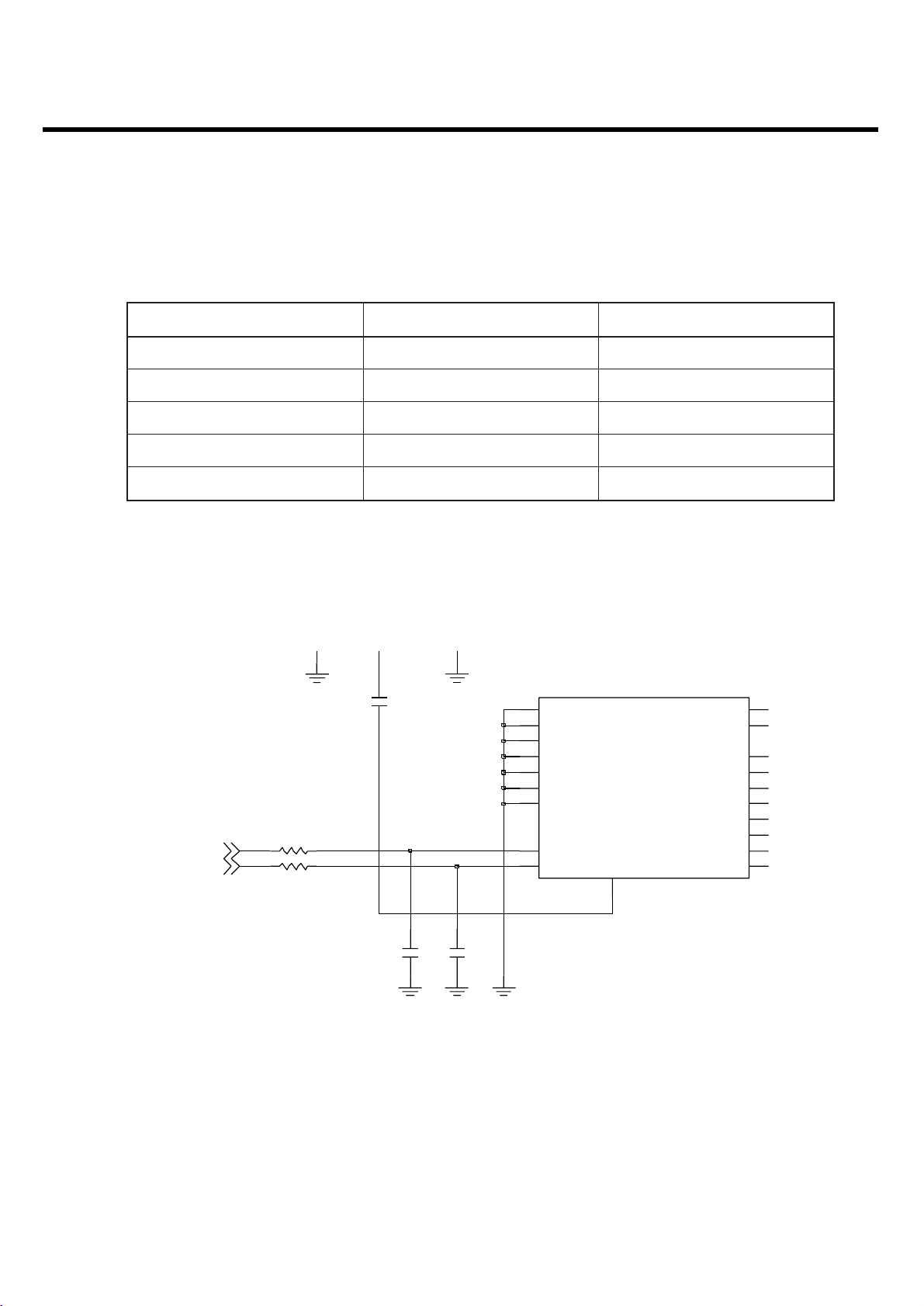
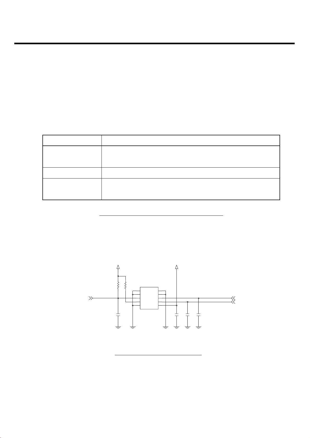
D. SIM interface
The AD6720 provides SIM Interface Module. The AD6720 checks status periodically during
established call mode whether SIM card is inserted or not, but it doesn't check during deep Sleep
mode. In order to communicate with SIM card, 3 signals SIM_DATA, SIM_CLK,
SIM_RST(GPIO_23) are required. The descriptions about the signals are given by bellow Table 3-5
in detail.
Signals Description
SIM_DATA
This pin receives and sends data to SIM card.
This model can support only 3.0 volt interface SIM card.
SIM_CLK Clock 3.25MHz frequency.
SIM_RST
Reset SIM block
(GPIO_23)
Table 3-5. SIM CONTROL SIGNALS DESCRIPTION
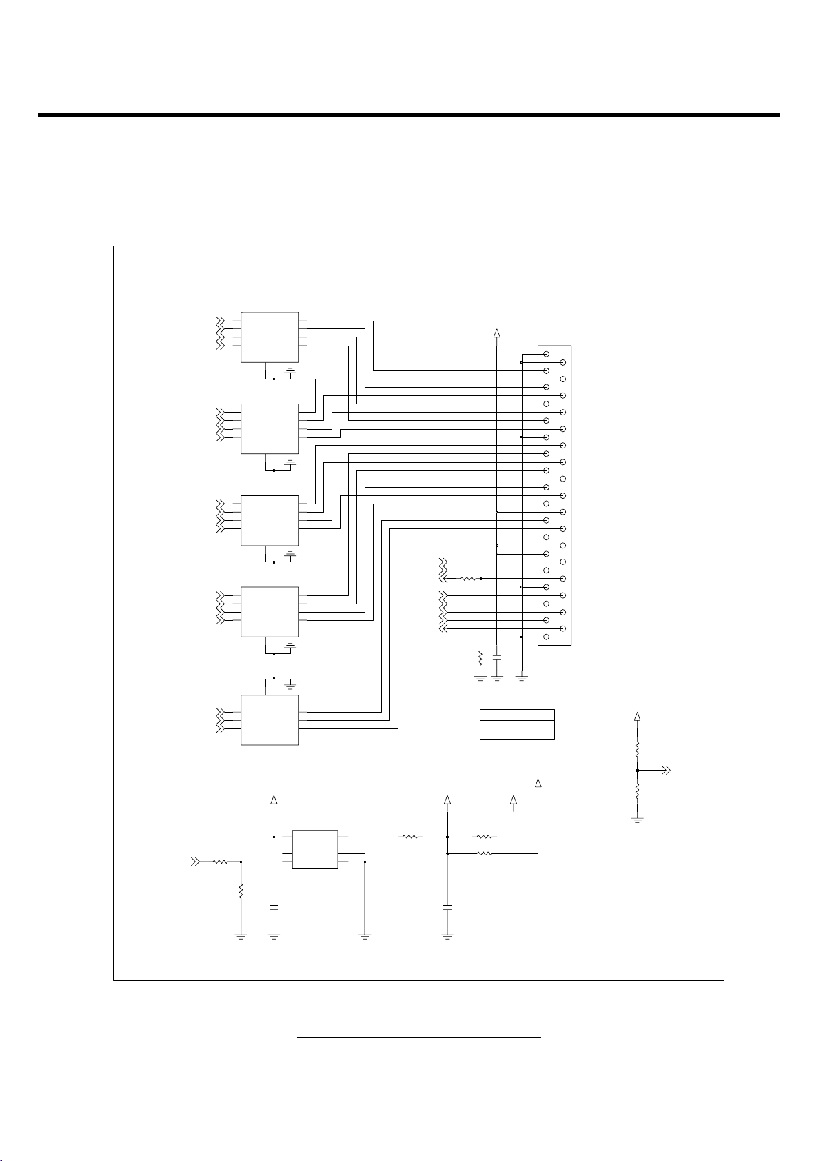
Figure 3-5. SIM Interface of AD6720
SIM CONNECTOR
220n
C317
R303
NA
NA
C319
2V85_VSIM
3
CLK
GND1
4
7
GND2
GND3
89
GND4
GND5
10
6
IO
RST
2
VCC
1
5
VPP
ENSY0014601
J300
HSSC-6p-23
1000p
C318
C316
NA
2V85_VSIM
R315
15K
SIM_CLKSIM_DATA
SIM_RST

3. TECHNICAL BRIEF
- 26 -
E. LDO Block
There are 8 LDOs in the AD6720.
- VCORE : supplies Digital baseband Processor core and AD6720 digital core
- VMEM : supplies external memory and the interface to the external memory on the digital
baseband processor (1,8V or 2.8V, 150mA)
- VEXT : supplies Radio digital interface and high voltage interface (2.8V, 170mA)
- VSIM : supplies the SIM interface circuitry on the digital processor and SIM card (2.85V, 20mA)
- VRTC : supplies the Real-Time Clock module (1.8 V, 20 µA)
- VABB : supplies the analog portions of the AD6720
- VMIC : supplies the microphone interface circuitry (2.5 V, 1 mA)
- VVCXO : supplies the voltage controlled crystal oscillator ( 2.75 V, 10 mA)
3.6 Battery Charging Block
1. It can be used to charge Lithium Ion batteries.
Charger initialization, trickle charging, and Li-Ion charging control are implemented in hardware.
2. Charging Process
- Check charger is inserted or not
- If AD6720 detects that Charger is inserted, the CC-CV charging starts.
- Exception : When battery voltage is lower than 3.2V, the precharge(low current charge mode)
starts firstly.
- And the battery voltage reach to 3.2V the CC-CV charging starts.
3. Pins used for charging
- VCHG : charger supply.
- GATEDRIVE : charge DAC output
- ISENSE : charge current sense input
- VBATSENSE : battery voltage sense input.
- BATTYPE : battery type identification input
- REFCHG : voltage reference output
4. TA (Travel Adaptor)
- Input voltage: AC 85V ~ 260V, 50~60Hz
- Output voltage: DC 5.2V (0.2 V)
- Output current: Max 800mA (50mA)
5. Battery
- Li-ion battery (Max 4.2V, Nom 3.7V)
- Standard battery: Capacity - 830mAh
3. TECHNICAL BRIEF
- 27 -
Figure 3-6. CIRCUIT FOR BATTERY CHARGING
PRE
CHARGING
NORMAL
CHARGING
VCHARGE
VBAT
ECCH0000182
R217
10K
R211
0
Q201
31
2
UMX1NTN
R214
1K
4
56
R216
7.5K
C224
0.1u
PRE_CHARGE_R INDLED_R
R215
1.5K
R218
10K
GATEDRV
ISENSE
C225
1u
10V Under
VBAT
R212
0.2
ECCH0004904
R213
330
Q200
G5S
4
D36D4
3
D2
D5
2
D1
D6
1
TPCF8102-TE85L-F
VCHARGE
D200
CUS02
7
8
C223
4.7u
10V Over
ECCH0005704
3. TECHNICAL BRIEF
- 28 -
3.7 Display and Interface
• Main LCD
Controlled by L_MAIN_LCD_CS, LCD_RESET, LCD_RS, LCD_WR, LCD_RD, IFMODE,
L_DATA[00:15] ports
• L_MAIN_LCD_CS : MAIN LCD driver chip enable. MAIN LCD driver IC has own CS pin
• LCD_RST : This pin resets LCD module. This signal comes from AD6720 directly.
• LCD_RS: This pin determines whether the data to LCD module are display data or control data.
• L_WR : Write control Signal
• L_RD : Read control Signal. But this pin used only for debugging.
• L_DATA[00:15] : Parallel data lines.
• LCD_ID[1:2] : LCD type selection signals
- LCD_ID1 : LCD maker(2.4V is BYD, 0V is LGIT)
- LCD_ID[2:3] : for the future using
• For using 262K color, data buses should be 16 bits.
Properties Spec. Unit
Active Screen Size 28.032*35.04 mm
Color Depth 262,144 colors
Resolution 128 X RGB X 160 dots
3. TECHNICAL BRIEF
- 29 -
L_DATA00
Figure 3-7. LCD INTERFACE CIRCUIT
L_DATA02
L_DATA04
L_DATA06
(50 ohm, 15pF)
L_DATA01
L_DATA03
L_DATA05
L_DATA07
(50 ohm, 15pF)
L_DATA08
L_DATA10
L_DATA12
L_DATA14
(50 ohm, 15pF)
L_DATA09
L_DATA11
L_DATA13
L_DATA15
(50 ohm, 15pF)
L_MAIN_LCD_CS
LCD_RS
LCD_WR
(50 ohm, 15pF)
* NA : U103, C110
LCD_LDO_EN
LCD CONNECTOR 35pin(ZIP)
FL101
R113
4.7K
R115
100K
1
2
3
4
1
2
3
4
1
2
3
4
1
2
3
4
4
3
2
1
EVRC14S03Q030050R
INOUT_A1
INOUT_A2
INOUT_A3
INOUT_A4
FL102
EVRC14S03Q030050R
INOUT_A1
INOUT_A2
INOUT_A3
INOUT_A4
FL103
EVRC14S03Q030050R
INOUT_A1
INOUT_A2
INOUT_A3
INOUT_A4
FL104
EVRC14S03Q030050R
INOUT_A1
INOUT_A2
INOUT_A3
INOUT_A4
INOUT_A4
INOUT_A3
INOUT_A2
INOUT_A1
FL105
EVRC14S03Q030050R
C110
9
INOUT_B1
8
INOUT_B2
7
INOUT_B3
6
INOUT_B4
G110G2
5
9
INOUT_B1
8
INOUT_B2
7
INOUT_B3
6
INOUT_B4
G15G2
10
9
INOUT_B1
8
INOUT_B2
7
INOUT_B3
6
INOUT_B4
G110G2
5
9
INOUT_B1
8
INOUT_B2
7
INOUT_B3
6
INOUT_B4
G15G2
10
5G110
G2
INOUT_B4
6
INOUT_B3
7
INOUT_B2
8
INOUT_B1
9
VBAT
U103
1
VDD3VOUT
4
GND1
NC
6
CE
GND2
R1114D281D-TR-F
1u
* CON Pin 16, LCD Pin 20 : _LCD_RD
2
5
LCD_RESET
IF_MODE
LCD_ID
MLED
MLED1
MLED2
MLED3
VSYNCOUT
2V8_VLCD 2V8_VCAM
R110
NA
C112
1u
2V8_VLCD
R106
100K
R107
100K
R111 0
C109
1u
IF_MODE
H
L
NAR112
CN101
35
33
31
29
27
25
23
21
19
17
15
13
11
XF2B-3545-31A-P
ENQY0010901
9671S-35A-GF
LCD IF
9 BIT I/F
16BIT I/F
2V8_VEXT
* LCD CON : Top Contact Type
34
32
30
28
26
24
22
20
18
16
14
12
10
9
8
7
6
5
4
3
2
1
2V8_VLCD
NA
47K
R108
R109
IF_MODE
10V Under
ECCH0004904
ECCH0004904
3. TECHNICAL BRIEF
- 30 -
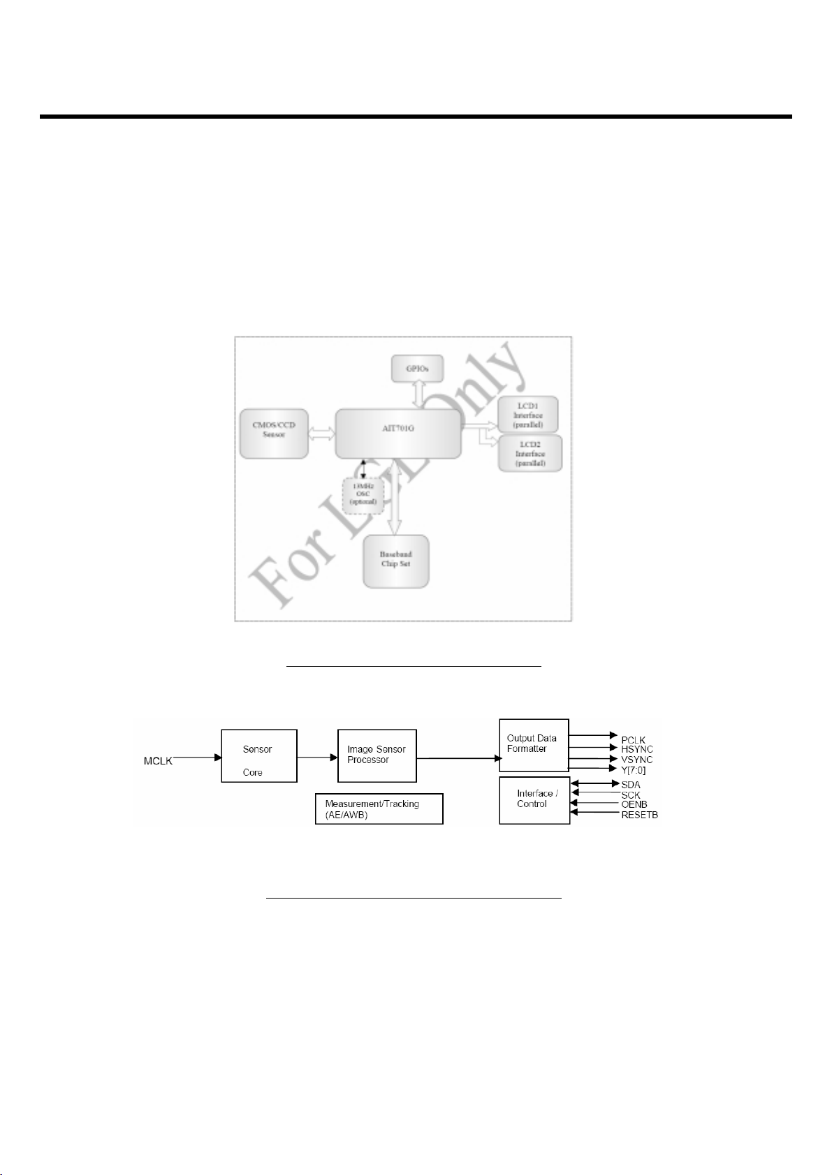
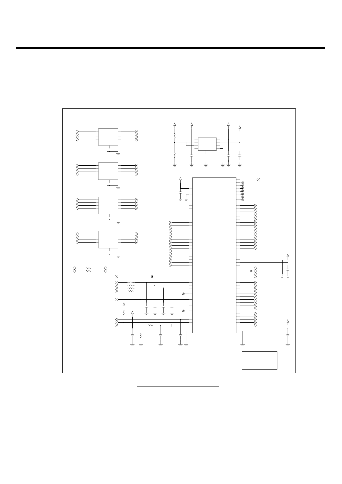
3.8 Camera IC(AIT701G , U401)
This model has a built-in VGA(640 x 480) camera module. And the camera produces JPG pictures.
Camera module is controlled by AIT701G. Interface is done by I2C and YCbCr format. I2C is a control
signal and YCbCr is real data interface signal.
Figure 3-8. AIT701G BLOCK DIAGRAM
Figure 3-9. SENSOR CHIP BLOCK DIAGRAM
3. TECHNICAL BRIEF
- 31 -
Figure 3-10. AIT701G CIRCUIT
CAM_PWR_EN
ACTIVELOW
DEACTIVE
STATUS
10V Under
CAMERA CTL IC
HIGH
15p 100 15p
TP403
TP404
2V8_VCAM
TP407
7.5p
C424
TP405
5
G110G2
1
INOUT_A1
INOUT_A2
2
3
INOUT_A3
INOUT_A4
4
INOUT_B1
9
8
INOUT_B2
INOUT_B3
7
6
INOUT_B4
1u
SFEY0013201
EVRC14S03Q030100RFL403
ECCH0004904
C400
R428 100ohm
NA
R403
C420
NA
7.5p
C426
R421
100K
0R427
100ohmR429
R430 100ohm
2V8_VCAM
C417
TP401
33p
CAM_INT
C425
7.5p
VBAT
R426 0
100ohmR425
TP406
C422
1uF
0.01u
C403
C404
1u
1V8_VCAM
VDD_IO2
E8
B3
PLCD_A0
A3
PLCD_RD_
PLCD_WE_
A4
PMCLK
J2 F1
PPXL_CLK
K3
PRST_
D3
PSCAN_EN
PSCK
G2
PSDA
H2
H1
PSEN
PS_RST_
F2
PTEST_EN
E10
G1
PVSYNC
H5
VDD_CORE
G3
VDD_IO0 VDD_IO1
H8
B5
PLCD12
PLCD13
A6
PLCD14
C4
A5
PLCD15
PLCD16
B4
C3
PLCD17
PLCD1_CS_
B2
A9
PLCD2
PLCD2_CS_
A2
C9
PLCD3
PLCD4
D8
PLCD5
A8
PLCD6
B8
PLCD7
C8
C7
PLCD8
PLCD9
C6
PHD7
J6
PHD8
K10
J9
PHD9
PHGPIO_CS_
J10
PHINT
J8
PHLCD2_CS_
K8
J7
PHLCD_A0
K7
PHLCD_BY
J1
PHRD_
E3
PHSYNC
K9
PHWAIT_
PHWE_
K2
PLCD0
A10
PLCD1
B10
PLCD10
B6
C5
PLCD11
F9
PGPIO6
PGPIO7
D10
K1
PHCS_
J3
PHD0
H3
PHD1
PHD10
H10
H9
PHD11
PHD12
G10
G9
PHD13
PHD14
G8
PHD15
F10
PHD2
K4
PHD3
J4
K5
PHD4
J5
PHD5
PHD6
K6
GND_IO2
F8
PD0
E2
E1
PD1
D1
PD2
PD3
D2
PD4
C2
C1
PD5
A1
PD6
B1
PD7
F3
PDCLK
E9
PGPIO0
D9
PGPIO1
PGPIO2
C10
B9
PGPIO3
A7
PGPIO4
B7
PGPIO5
U401 AIT701G
GND_CORE
H6
GND_IO0
H4 H7
GND_IO1
TP400
R431 0
1u
ECCH0004904
C401
INOUT_B3
INOUT_B4
6
FL401 EVRC14S03Q030100R
SFEY0013201
G15G2
10
INOUT_A1
1
2
INOUT_A2
INOUT_A3
3
4
INOUT_A4
9
INOUT_B1
INOUT_B2
8
7
4
INOUT_A4
9
INOUT_B1
INOUT_B2
8
7
INOUT_B3
INOUT_B4
6
2V8_VCAM
FL404 EVRC14S03Q030100R
SFEY0013201
G15G2
10
INOUT_A1
1
2
INOUT_A2
INOUT_A3
3
R400
100K
2V8_VCAM
CAM_HOLD
9
8
INOUT_B2
INOUT_B3
7
6
INOUT_B4
1V8_VCAM
EVRC14S03Q030100RFL402
5
G110G2
1
INOUT_A1
INOUT_A2
2
3
INOUT_A3
INOUT_A4
4
INOUT_B1
SFEY0013201
1u
ECCH0004904
C402
EN1
EN2
3
5
GNDNC1
4
NC2
6
PGND
9
VIN1VOUT1
8
7
VOUT2
RT9011-MGPQW
U400
2
C423
1uF
TP402
68K
R418
C418
2V8_VEXT
1000p
LCD_RD
2V8_VCAM
27p
C427
A_DATA09
_LCD_CS
ADD01
A_WR
A_RD
_RD
_WR A_WR
A_RD
13M_AIT_DBB
A_DATA00
A_DATA01
A_DATA10
A_DATA11
A_DATA12
A_DATA13
A_DATA14
A_DATA15
A_DATA02
A_DATA03
A_DATA04
A_DATA05
A_DATA06
A_DATA07
A_DATA08
DATA05
DATA04
DATA11
DATA10
DATA09
DATA08
DATA15
DATA14
DATA13
DATA12
C_SDA
DATA03
DATA02
DATA01
DATA00
DATA07
DATA06
_WAIT
VSYNCOUT
C_HS
A_DATA03
A_DATA04
A_DATA05
A_DATA06
A_DATA07
A_DATA08
A_DATA09
L_MAIN_LCD_CS
L_DATA07
L_DATA08
L_DATA09
LCD_RD
LCD_WRCAM_HOLD
CAM_RST
A_DATA00
A_DATA01
A_DATA10
A_DATA11
A_DATA12
A_DATA13
A_DATA14
A_DATA15
A_DATA02
C_SCK
C_VS
LCD_RS
L_DATA00
L_DATA01
L_DATA10
L_DATA11
L_DATA12
L_DATA13
L_DATA14
L_DATA15
L_DATA02
L_DATA03
L_DATA04
L_DATA05
L_DATA06
C_CD00
C_CD01
C_CD02
C_CD03
C_CD04
C_CD05
C_CD06
C_CD07
C_MCLK
C_PCLK
CAM_PWR_EN
C_RST
 Loading...