

LG MG191A Service Manual

lau
naMec
i
v
re
S
:
l
edo
MMG191a
Service Manual
MG191a
P/N : MMBD0048101 Date : April 2005
REVISED HISTORY
Editor Date IssueContents of Changes S/W Version
Y.M. CHO 29/DEC/2003 Issue 0.1 INITIAL RELEASE
Y.M. CHO 25/JAN/2004 Issue 0.2 SECOND RELEASE
* The information in this manual is subject to change without notice and should not be construed as a
commitment by LGE Inc. Furthermore, LGE Inc. reserves the right, without notice, to make changes to
equipment design as advances in engineering and manufacturing methods warrant.
* This manual provides the information necessary to install, program, operate and maintain the MG191a.
-
1
-


Table of Contents
1. Introduction ................................. 5
1.1. Purpose
1.2. Regulatory Information ......................5
1.2.1. Security ...................................... 5
1.2.2. Incidence of Harm ...................... 5
1.2.3. Changes in Service .................... 5
1.2.4. Maintenance Limitations ............. 5
1.2.5. Notice of Radiated Emissions .... 6
1.2.6. Pictures ....................................... 6
1.2.7. Interference and Attenuation ...... 6
1.2.8. Electrostatic Sensitive Devices ... 6
1.3 Abbreviation ....................................... 6
.............................................5
2. General Performance ................. 8
2.1. H/W Feature ..................................... 8
2.2. Technical Specification ................... 10
3.3. Analog Baseband(ABB) Processor.. 23
3.3.1. General Description .................. 23
3.3.2. Audio Signal Processing &
Interface ................................... 24
3.3.3. Baseband Codec (BBC) ........... 25
3.3.4. Voltage Regulation (VREG) ..... 26
3.3.5. ADC Channels .......................... 27
3.3.6. Charging ................................... 28
3.3.7. Switch ON/OFF ......................... 29
3.3.8. Memory
3.3.9. Display & FPC Interface ......... 29
3.3.10. Keypad Switching &
Scanning ................................. 31
3.3.11. Audio ....................................... 32
3.3.12. Keypad back-light
Illumination ............................. 35
3.3.13. LCD Illumination ..................... 35
.................................. 29
3. H/W Circuit Description ............ 15
3.1. RF Circuit ........................................ 15
3.1.1. Front End Part .......................... 15
3.1.2. Receiver Part ............................ 16
3.1.3. Synthesizer Part ....................... 17
3.1.4. Transmitter Part ........................ 17
3.1.5. Power Amplifier ......................... 18
3.1.6. 26 MHz Clock ........................... 18
3.2. Digital Baseband(DBB) Processor
3.2.1. General Description .................. 19
3.2.2. Block Description ...................... 23
3.2.3. External Devices connected to
memory interface ...................... 21
3.2.4. RF Interface
...................... 21
block)
TSP
(TPU,
3.2.5. SIM interface ............................ 21
3.2.6. UART Interface ........................ 22
3.2.7. GPIO map
................................ 23
.
. 19
3.4. Camera Circuit ................................ 36
A. BaseBand Components
(Component Side)
B. BaseBand Components
(Keypad Side) ................................ 37
Digital Baseband (DBB)
C.
Processor ....................................... 37
D. Analog Main Processor (ABB) ....... 38
E. Memory
F. Voltage Regulation (LDO) .............. 40
G. MIDI ............................................... 41
H. Charging ......................................... 41
I. KEY Back-light Illumination .............. 42
J. SIM
K. Keypad
.......................................... 39
.................................................. 42
........................................... 43
.......................... 36
-
3
-

4. TROUBLE SHOOTING ................ 44
4.1. Baseband Components
(Component Side) ........................... 44
4.2. Baseband Components
(Keypad Side + Button Side) .......... 45
4.3. Power On Trouble ........................... 46
4.4. Charging Trouble ............................ 47
4.5. LCD Display Trouble ....................... 49
4.6. Speaker/Receiver Trouble .............. 51
A. Receiver Trouble ............................ 53
B. Speaker Trouble ............................. 53
4.7. Microphone Trouble ........................ 54
4.8. Vibrator Trouble .............................. 55
4.9. Keypad Backlight Trouble ............... 57
4.10. SIM Detect Trouble ....................... 59
4.11. Earphone Trouble ......................... 61
4.12. The Block Diagram of
the RF Part ................................... 64
4.13. Tx / Rx Part Description ............... 66
9. STAND ALONE TEST &
CALIBRATION ........................ 103
A. What is Standalone Test? ............ 103
B. Standalone Test
Equipment Setup ...............
C. Rx Standalone Test ...................... 104
D. Tx Standalone Test ...................... 104
E. What is Calibration? ..................... 105
F. Calibration program ...................... 106
G. Calibration Equipment Setup ....... 107
H. Calibrate MG191a with ChiWoo ... 108
............... 103
10. EXPLODED VIEW &
REPLACEMENT PART LIST ... 113
10.1. EXPLODED VIEW .......................... 113
10.2. Replacement Parts
<Mechanic component> .................... 115
10.2. Replacement Parts
<Main component> ........................... 117
10.3. Accessory ....................................... 128
4.14. Receiver Part Description ............. 67
4.15. Transmitter Part Description ......... 71
4.16. RX Part Trouble Shooting ............. 74
4.17. TX Part Trouble Shooting ............. 80
5. DOWNLOAD AND
CALIBRATION ............................ 85
6. BLOCK DIAGRAM ...................... 91
7. CIRCUIT DIAGRAM .................... 95
8. PCB LAYOUT............................. 100
- 4 -

1. INTRODUCTION
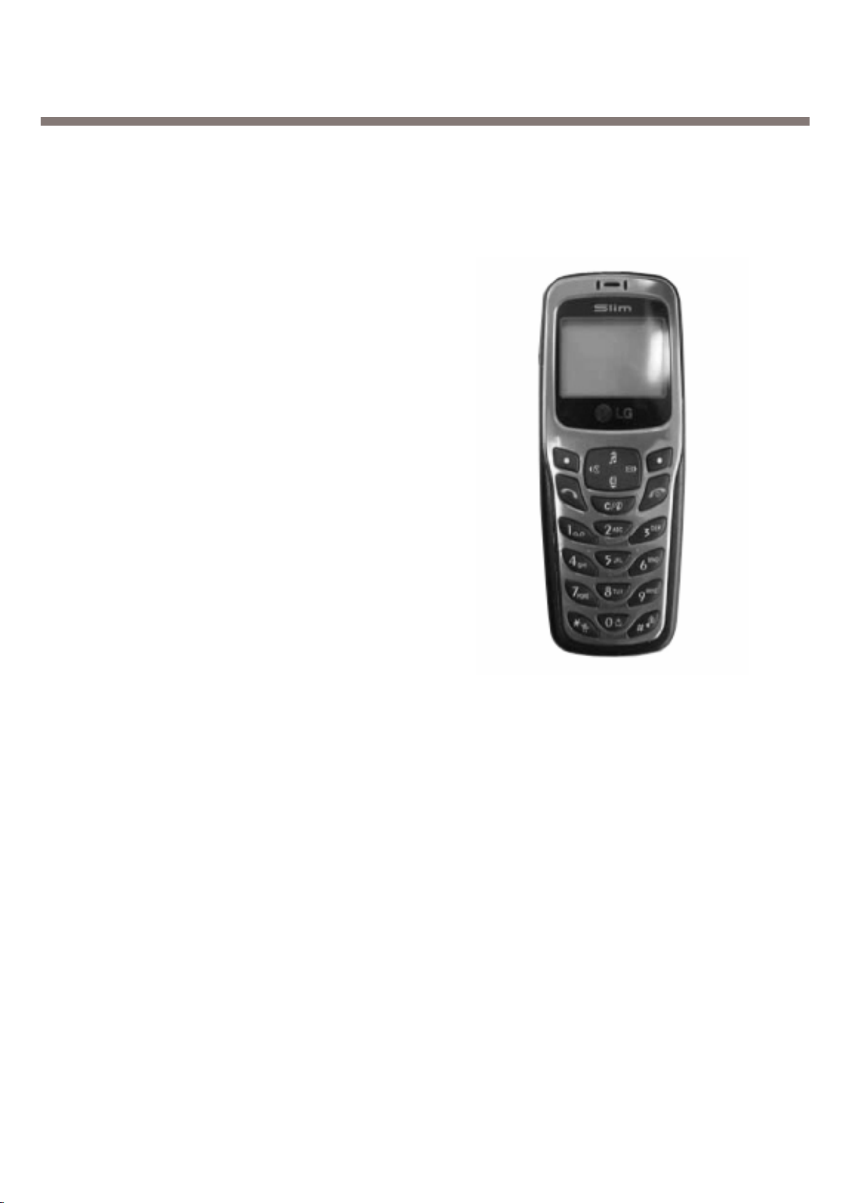
1. Introduction
1.1. Purpose
This manual provides the information necessary to repair, calibration, description and download the
features of the MG191a.
1.2. Regulatory Information
1.2.1. Security
Toll fraud, the unauthorized use of telecommunications system by an unauthorized part (for example,
persons other than your company’s employees, agents, subcontractors, or person working on your
company’s behalf) can result in substantial additional charges you’re your telecommunications
services. System users are responsible for the security of own system. There are may be risks of toll
fraud associated with your telecommunications system. System users are responsible for
programming and configuring the equipment to prevent unauthorized use. LGE does not warrant that
this product is immune from the above case but will prevent unauthorized use of common-carrier
telecommunication service of facilities accessed through or connected to it. LGE will not be
responsible for any charges that result from such unauthorized use.
1.2.2. Incidence of Harm
If a telephone company determines that the equipment provided to customer is faulty and possibly
causing harm or interruption in service to the telephone network, it should disconnect telephone
service until repair can be done.
as repair is not done.
A telephone company may temporarily disconnect service as long
1.2.3. Changes in Service
local telephone company may make changes in its communications facilities or procedure. If these
A
changes could reasonably be expected to af
network, the telephone company is required to give advanced written notice to the user
user to take appropriate steps to maintain telephone service.
fect the use of the MG191a or compatibility with the
, allowing the
1.2.4. Maintenance Limitations
Maintenance limitations on the MG191a must be performed only by the LGE or its authorized agent.
The user may not make any changes and/or repairs expect as specifically noted in this manual.
Therefore, note that unauthorized alternations or repair may affect the regulatory status of the system
and may void any remaining warranty
.
-
5
-

1. INTRODUCTION
APC Automatic Power Control
BB Baseband
BER Bit Error Ratio
CC-CV Constant Current ? Constant Voltage
CLA Cigar Lighter Adapter
DAC Digital to Analog Converter
DCS Digital Communication System
dBm dB relative to 1 milliwatt
DSP Digital Signal Processing
EEPROM Electrical Erasable Programmable Read-Only Memory
1.2.5. Notice of Radiated Emissions
The MG191a complies with rules regarding radiation and radio frequency emission as defined by loca
regulatory agencies. In accordance with these agencies, you may be required to provide information
such as the following to the end user.
1.2.6. Pictures
The pictures in this manual are for illustrative purposes only; your actual hardware may look slightly
different.
1.2.7. Interference and Attenuation
An MG191a may interfere with sensitive laboratory equipment, medical equipment, etc. Interference
from unsuppressed engines or electric motors may cause problems.
1.2.8. Electrostatic Sensitive Devices
ATTENTION
Boards, which contain Electrostatic Sensitive Device (ESD), are indicated by the sign. Following
information is ESD handling: Service personnel should ground themselves by using a wrist strap
when exchange system boards.
When repairs are made to a system board, they should spread the floor with anti-static mat which is
also grounded. Use a suitable, grounded soldering iron. Keep sensitive parts in these protective
packages until these are used. When returning system boards or parts such as EEPROM to the
, use the protective package as described.
factory
1.3 Abbreviation
Para os propósitos do manual, a seguir as abreviações aplicadas.
-
6
-
EL Electroluminescence
ESD
Electrostatic Discharge
FPCB
Flexible Printed Circuit Board
GMSK Gaussian Minimum Shift Keying
GPIB General Purpose Interface Bus
GPRS General Packet Radio Service
GSM Global System for Mobile Communications
IPUI International Portable User Identity
IF Intermediate Frequency
LCD Liquid Crystal Display
LDO Low Drop Output
LED Light Emitting Diode
LGE LG Electronics
OPLL Offset Phase Locked Loop
PAM Power Amplifier Module
PCB Printed Circuit Board
PGA Programmable Gain Amplifier
PLL Phase Locked Loop
PSTN Public Switched Telephone Network
RF Radio Frequency
RLR Receiving Loudness Rating
RMS Root Mean Square
RTC Real Time Clock
SAW Surface Acoustic Wave
SIM Subscriber Identity Module
SLR Sending Loudness Rating
SRAM Static Random Access Memory
STMR Side Tone Masking Rating
TA Travel Adapter
TDD Time Division Duplex
TDMA Time Division Multiple Access
UART Universal Asynchronous Receiver/Transmitter
VCO Voltage Controlled Oscillator
VCTCXO Voltage Control Temperature Compensated Crystal Oscillator
WAP Wireless Application Protocol
-
7
-
1. INTRODUCTION
2. General Performance
2. General Performance
2.1 H/W Feature
A. Hardware Feature
• GSM 850 / PCS 1900 Dual Band
• Mono(120x64) Single LCD
• 830mAh Li-Ion Battery
• 3V plug-in type SIM card socket
• 40 poly MIDI sound Ring-tone
• Jack type Ear-microphone
• Dimension : 103.3 x 42.8 x 15.5mm, Weight : 68 g
B. Software Feature
• WAP Supported
• GPRS Class 10 Compatible
• FR/EFR Speech Coding
• 5-Level Volume Control (Voice, Ringtone, etc..)
• SMS
• Phone Book
–255 entries
• Language : English & Spanish
• T9 Text
-
8
-
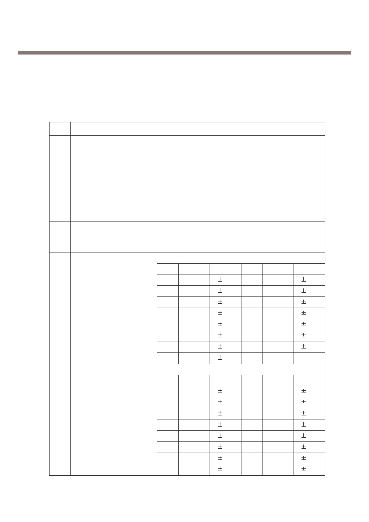
2. General Performance
ItemFeature
Standard Battery Li-ion, 830mAh
AVG TCVR Current GSM850: 250mA, PCS: 200mA
Standby Current < 4.0mA
Talk time < 4 hours (GSM TX Level 7), 3hours 30min
Standby time 200 hours (Paging Period 2, RSSI:-85dBm)
Charging time 2.5 hours
RX Sensitivity GSM850 : -108dBm, PCS : -107dBm
TX output power GSM850: 33dBm (Level 5)
PCS190: 30dBm (Level 0)
GPRS compatibility Class 10
SIM card type 1.8V/3V Small
Display 120 x 64 dots LCD
Soft icons
Key Pad
Status Indicator 0 ~ 9, #, *, Navigation Key, Menu Key,
Confirm Key,
Send Key, END/PWR Key
ANT Internal
EAR Phone Jack 3 pole earphone jack
PC Synchronization Yes
Speech coding EFR/FR
Data and Fax Yes
Vibrator Yes
Buzzer No
Voice Recoding Yes
C-Mic Yes
Receiver Yes
Travel Adapter Yes
Options No
MP(-104 dBm)
႘ၸ
Comment
Size:4.3(T)x34(W)x50(L)mm
Weight: 17g
-
9
-
2. General Performance
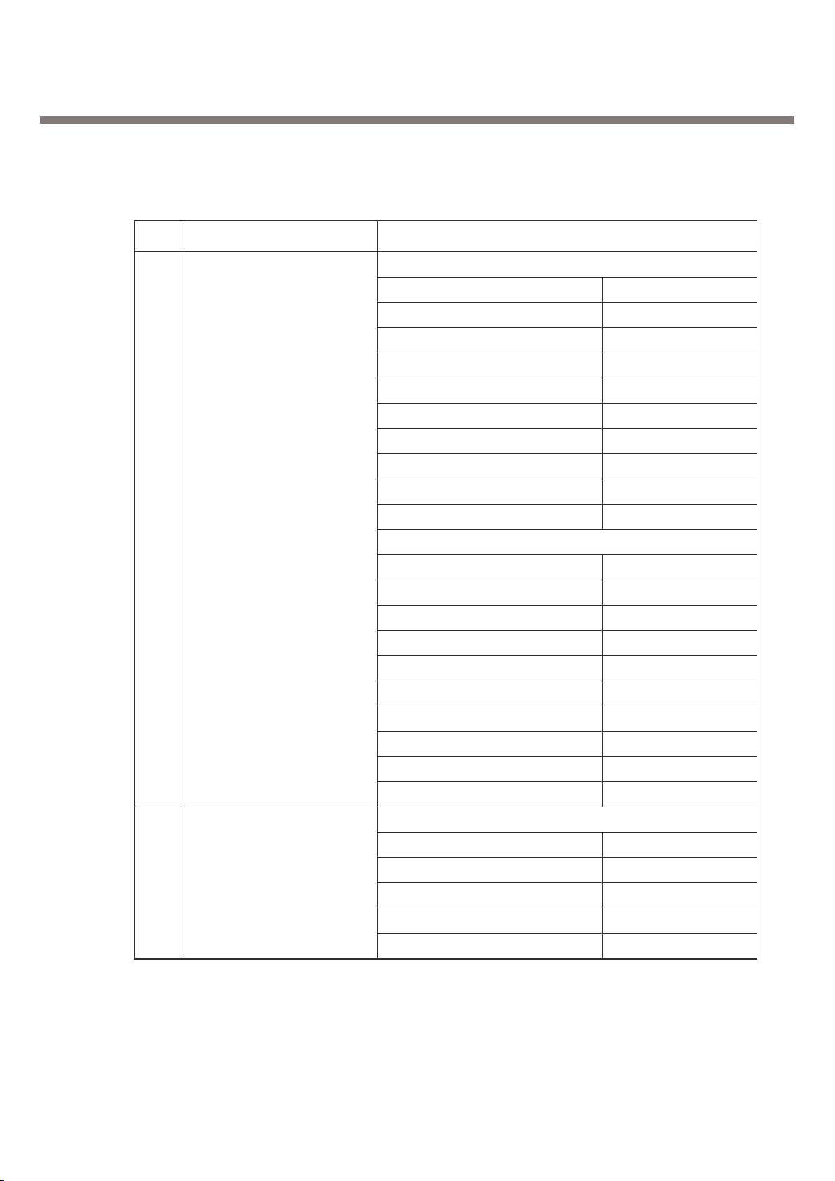
Item Description Specification
GSM 850 TX : 824-849Mhz
1 Frequency Band
2 Phase Error
RMS < 5 degrees
Peak < 20 degrees
3 < 0.1ppm
GSM850
Level Power Toler. Level Power Toler.
5 33 dBm 2dB 13 17 dBm 3dB
6 31 dBm 3dB 14 15 dBm 3dB
7 29 dBm 3dB 15 13 dBm 3dB
8 27 dBm 3dB 16 11 dBm 5dB
9 25 dBm 3dB 17 9 dBm 5dB
10 23 dBm 3dB 18 7 dBm 5dB
11 21 dBm 3dB 19 5 dBm 5dB
4 12 19 dBm 3dB
PCS
Level Power Toler. Level Power Toler.
0 30 dBm 2dB 8 14 dBm 3dB
1 28 dBm 3dB 9 12 dBm 4dB
2 26 dBm 3dB 10 10 dBm 4dB
3 24 dBm 3dB 11 8 dBm 4dB
4 22 dBm 3dB 12 6 dBm 4dB
5 20 dBm 3dB 13 4 dBm 4dB
6 18 dBm 3dB 14 2 dBm 5dB
7 16 dBm 3dB 15 0 dBm 5dB
Frequency Error
Power Level
GSM 850 RX : 869-894Mhz
PCS 1900 RX : 1930-1990Mhz
PCS 1900 TX : 1850-1910Mhz
2.2 Technical Specification
10
-
-
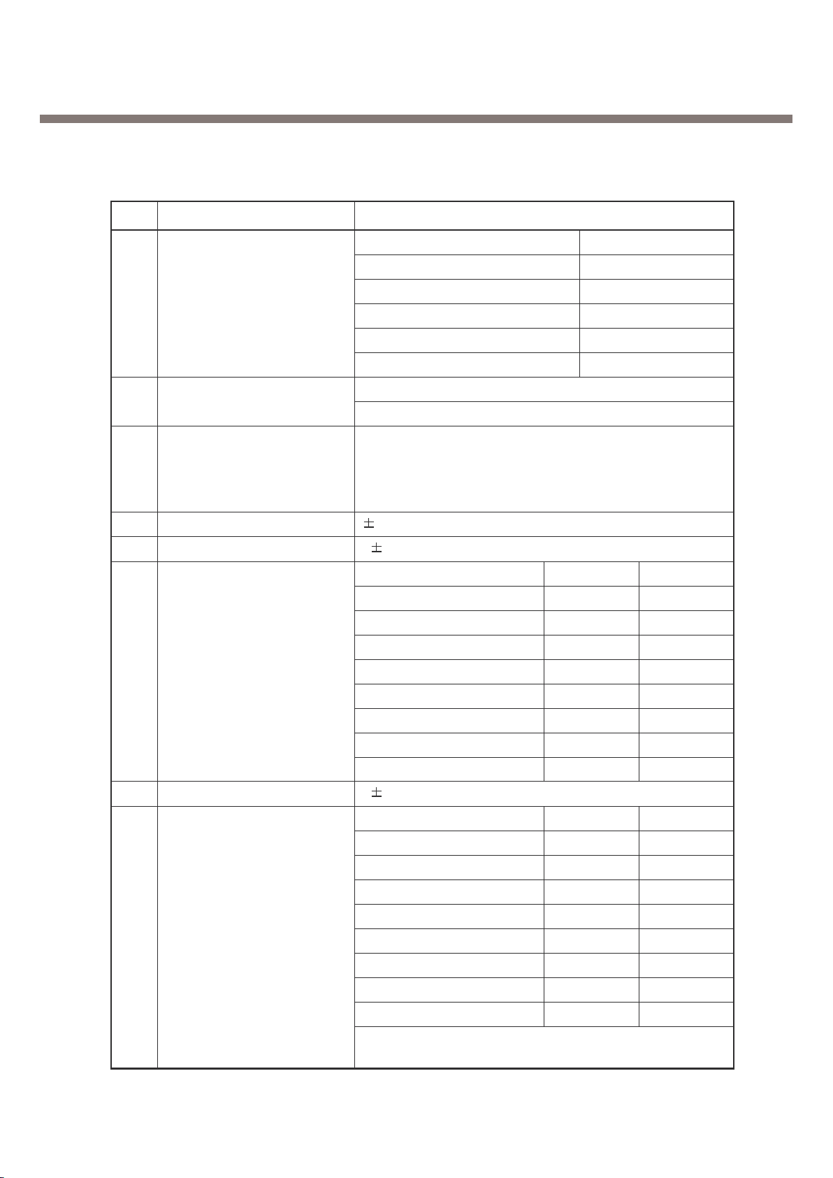
GSM850
Offset from Carrier (kHz) Max. dBc
100 +0.5
200 -30
250 -33
400 -60
600 ~ 1,200 -60
1,200 ~ 1,800 -60
1,800 ~ 3,000 -63
3,000 ~ 6,000 -65
5
Output RF Spectrum 6,000 -71
(due to modulation) PCS
Offset from Carrier (kHz) Max. dBc
100 +0.5
200 -30
250 -33
400 -60
600 ~ 1,200 -60
1,200 ~ 1,800 -60
1,800 ~ 3,000 -65
3,000 ~ 6,000 -65
6,000 -73
GSM850
Offset from Carrier (kHz) Max. (dBm)
Output RF Spectrum 400 -19
6
(due to switching transient) 600 -21
1,200 -21
1,800 -24
Ite
m Description Specification
2. General Performance
-
11
-
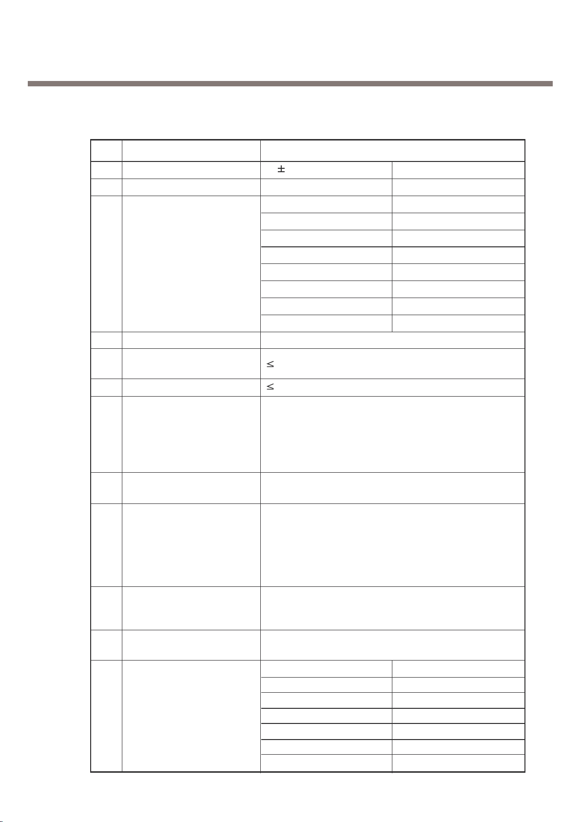
2. General Performance
PCS
Offset from Carrier (kHz) Max. (dBm)
Output RF Spectrum 400 -22
6
(due to switching transient) 600 -24
1,200 -24
1,800 -27
7 Spurious Emissions
Conduction, Emission Status
Conduction, Emission Status
GSM850
8 Bit Error Ratio
BER (Class II) < 2.439% @-102dBm
PCS
BER (Class II) < 2.439% @-100dBm
9 Rx Level Report accuracy 3 dB
10 SRL 8 3 dB
Frequency (Hz) Max.(dB) Min.(dB)
100 -12 /
200 0 /
300 0 -12
11 Sending Response 1,000 0 -6
2,000 4 -6
3,000 4 -6
3,400 4 -9
4,000 0 /
12 RLR 2 3 dB
Frequency (Hz) Max.(dB) Min.(dB)
100 -12 /
200 0 /
300 2 -7
500
*
-5
13 Receiving Response 1,0000-5
3,000 2 -5
3,400 2 -10
4,000 2
*
Mean that Adopt a straight line in between 300 Hz and
1,000 Hz to be Max. level in the range.
Item Description Specification
-
12
-
14 STMR 13 5 dB
15 Stability Margin > 6 dB
dB to ARL (dB)Level Ratio (dB)
-35 17.5
-30 22.5
-20 30.7
16 Distortion
-10 33.3
0 33.7
7 31.7
10 25.5
17 Side tone Distortion Three stage distortion < 10%
18
<Change> System frequency
(26 MHz) tolerance
19
<Change> 32.768KHz tolerance
30ppm
2.5 ppm
Full power
Standby
- Normal Mode 4.0mA(Mix. power)
- Using Test mode on DSP Sleep function 6mA
20 Power consumption
< 250mA (GSM850) ; < 200mA (PCS)
21 Talk Time
GSM850/Lvl 7 (Battery Capacity 830mA):230 min
GSM850/Lvl 12(Battery Capacity 830mA):380 min
Under conditions, at least 200 hours:
1. Brand new and full 740mAh battery
22 Standby Time
2. Full charge, no receive/send and keep GSM in idle mode.
3. Broadcast set off.
4. Signal strength display set at 3 level above.
5. Backlight of phone set off.
At least 80 dB under below conditions:
23 Ringer Volume 1. Ringer set as ringer.
2. Test distance set as 50 cm
24 Charge Voltage
Fast Charge : < 500 mA
Slow Charge: < 60mA
Antenna Bar Number Power
5-85 dBm ~
4-90 dBm ~ -86 dBm
25 Antenna Display 3-95 dBm ~ -91 dBm
2-100 dBm ~ -96 dBm
1-105 dBm ~ -101 dBm
0 ~ -105 dBm
Item Description Specification
Ž
Ž
2. General Performance
-
13
-
2. General Performance
Item Description Specification
Battery Bar Number Voltage ( 0.03V)
0 3.61V~ 3.50V
26 Battery Indicator 1 3.71V ~ 3.62V
2 3.78V ~ 3.72V
3
4
3.92V ~ 3.79V
4.2V ~ 3.93V
27 Low Voltage Warning 3.62V 0.03V (Standby)
28 Forced shut down Voltage 3.35 0.03 V
1 Li-ion Battery
29 Battery Type Standard Voltage = 3.7 V
Battery full charge voltage = 4.2 V
Capacity: 830mAh
Switching-mode charger
30 Travel Charger Input: 100 ~ 240 V, 50/60Hz
Out put: 5.2V, 800mA
- 14 -
3. H/W Circuit Description
Table 3-1. The Logic and Current
VC1 CurrentVC2
GSM TX 2.4 ~ 2.8V 0V
2.4 ~ 2.8 V
0 V
8.0mA max
< 0.1mA
PCS TX
GSM/PCS RX
8.0mA max0 V
0 V
3. H/W Circuit Description
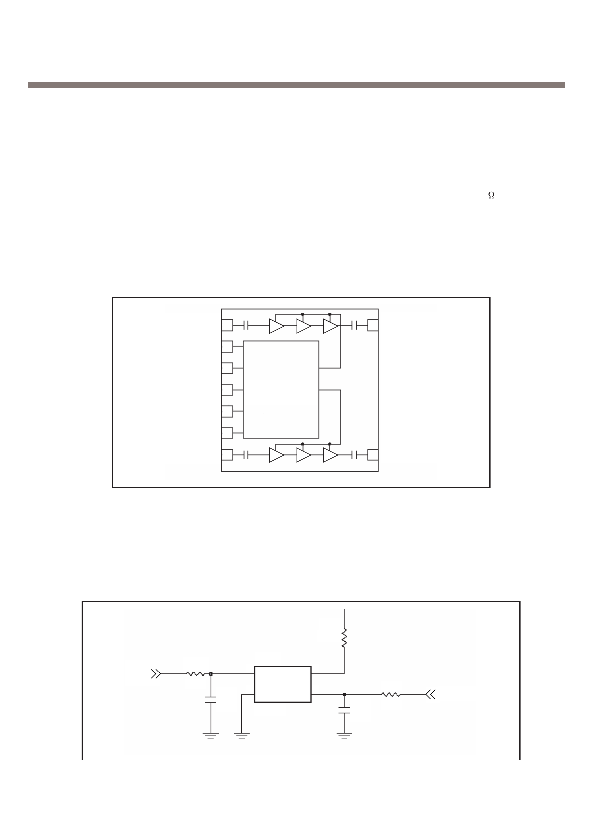
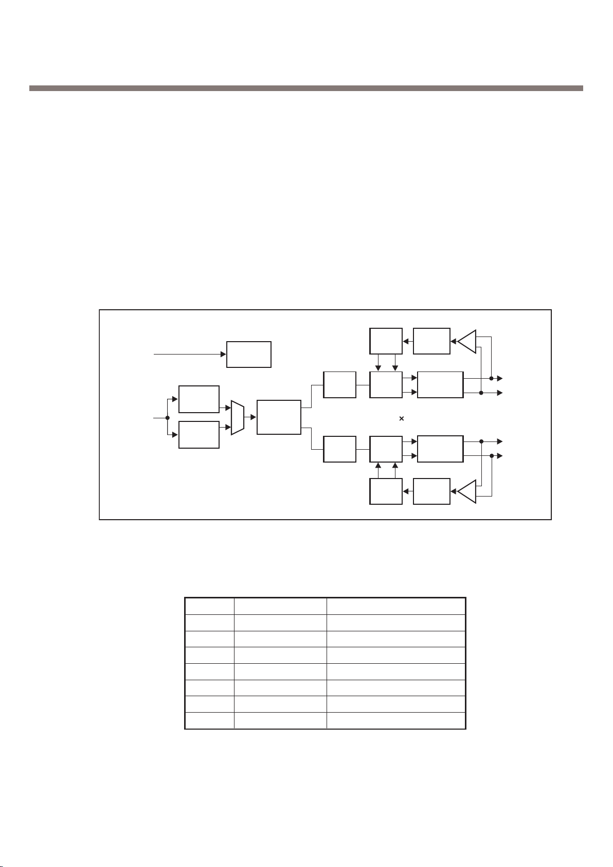
3.1. RF Circuit
The RF parts consist of a transmitter part, a receiver part, a frequency synthesizer part and a
VCTCXO part.
The TexasInstuments transceiver is composed of one RF chipset TRF6151C which is a quadrupleband GSM/GPRS wireless communications.
This device integrates a receiver based on direct conversion architecture, a transmitter based on
modulation-loop architecture, frequency synthesizing including a 26-MHzVCXO, a main N-integer
synthesizer, two main VCOs, a programmable main-loop filter, two TX VCOs, a TX loop filter, voltage
regulators to supply on-chip and off-chip RF functions, and a power-amplifier controller.
3.1.1. Front End Part
RF front end consists of Antenna Switch(FL502), dual band LNAs integrated in transceiver The
Received RF signals(GSM 869MHz ~ 894MHz, PCS 1930MHz ~ 1990MHz) are fed into the antenna
or mobile switch. An antenna matching circuit is between the antenna and the mobile switch. The
Antenna Switch is used for control the Rx and Tx paths. And, the input signals VC1 and VC2 of a
FL502, 1 are directly connected to baseband controller to switch either Tx or Rx path on. Ant S/W
module(FL502) is an antenna switch module for dual band phone. The logic and current is given
below Table 1.
RF saw filters consists of FL500, FL501. RF saw filters is Low-loss RF filter for mobile telephone
GSM850 and PCS systems. Input port Unbalanced to output port balanced operation.
-
15
-
3. H/W Circuit Description
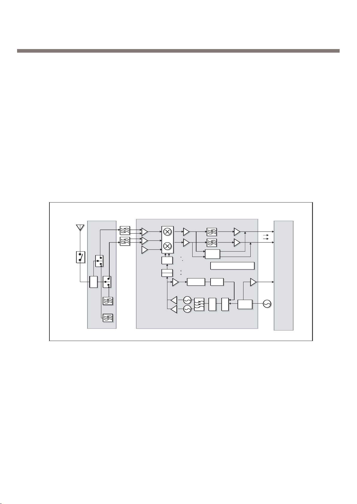
Figure 1. Receiver Part Block Diagram
U501/TRF6151
Baseband
(TI)
U101
+
U100
Calypso
Lite
FL500
Antenna Switch
LNA
FL50
1
FL50
2
SW500
Mobile
Switch
0••••/
90••••
D
I
P
PCS
PCS
DCS
GSM
GSM
VGA
1VGA3
DAC
5b
Serial interface
Prescaler
64/65
A/B
Count
MAIN VCO1
MAIN VCO2
CP
PFD
REF div
X500
VC-TCXO
26MHz
I
Q
0 /
90
4: GSM
2: PCS
3.1.2. Receiver Part
• A GSM850 LNA (LNAGSM) with switchable gain
• A PCS1900 LNA (LNAPCS) with switchable gain
• Demodulators for GSM850 (MIXGSM), PCS1900 (MIXPCS) bands with programmable gain
• Two baseband amplifiers with digitally-programmable gain
• Two fully-integrated baseband channel filters
• Two dc-offset compensation systems
• A divider by 4 for LO generation in GSM850 in order to minimize dc offset generated by self- mixing
and the LO reradiation
• A divider by 2 for LO generation in PCS1900 in order to minimize dc offset generated by self-mixing
and LO reradiation
-
-
16
3. H/W Circuit Description
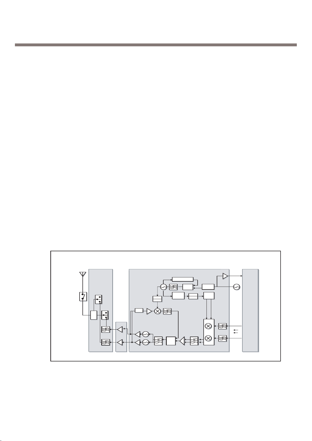
Figure 2. Transmitter Block Diagram
TX Block Diagram (GSM850+PCS1900)
U501/TRF6151
PAM
U503
RF3146
Baseband
(TI)
U101
IOTA
+
U100
Calypso
Lite
X500
VC-TCXO
26MHz
I
Q
N Divider
MAIN VCO
Phase
Comp
REF div
O · · /
90 · ·
Div
by 13
PAD
TX HB VCO
PFD
CP
TX LB VCO
PCS
GSM
FL500
Antenna Switch
SW500
Mobile
Switch
D
I
P
• 4
: GSM
• 2 : PCS
• 4
: GSM
• 2 : PCS
3.1.3. Synthesizer Part
• A 26-MHz VCXO with external
• A 26-MHz buffer to drive the DBBs
• Two main VCOs fully integrated
• A main N-integer synthesizer
• A programmable main loop filter
• Three voltage regulators to supply
• A digital serial interface
3.1.4. Transmitter Part
• Transceiver
Transmit section:
• An offset PLL with post-IQ modulator and post-offset mixer filters fully integrated on the chip
• Two TX VCOs fully integrated on the chip
• A TX loop filter fully integrated on the chip
• A divider by 4 for local oscillator (LO) generation in GSM900 and GSM850
• A divider by 2 for LO generation in DCS1800 and PCS1900
• A programmable M divider for IF generation
• A power-amplifier controller including all the functions required to design a power-sensing control
loop, except for the sensing diodes
17
-
-
3. H/W Circuit Description
BAND SELECT
TX ENABLE
VBATT
VBATT
DCS/PCS IN
VRAMP
GSM IN
DCS/PCS OUT
GSM OUT
40
41
42
43
37
37
37
45
48
Full
y Integrated
Power Control Circuit
Figure 3. Power Amp Block Diagram
AFC
R504
10K
C548
X500
VCONT
GND
26MHz
VCC
OUT
1 3
4
2
0.01u
R519
100
R523
TCXOEN
0
C558
1u
Figure 4. VC-TCXO Circuit
3.1.5. Power Amplifier
The RF3146[U501] is a high-power, high-efficiency power amplifier module with integrated power
control. The device is a self-contained 7mmx7mmx0.9mm lead frame module(LFM) with 50 input
and output terminals. The power control function is also incorporated, eliminating the need for
directional couplers, detector diodes, power control ASICs and other power control circuitry; this
allows the module to be driven directly from the DAC output. The device is designed for use as the
final RF amplifier in GSM850, EGSM900, DCS and PCS handheld digital cellular equipment and
other applications in the 824MHz to 849MHz, 880MHz to 915MHz, 1710MHz to 1785MHz and
1850MHz to 1910MHz bands.
3.1.6. 26 MHz Clock
The 26 MHz clock(X500) consists of a TCXO(Temperature Compensated Crystal Oscillator) which
oscillates at a frequency of 13 MHz. It is used within the TRF6151C RF Main Chip, BB Analog chipset(IOTA), Digital chip-set(Calypso Lite).
-
18
-
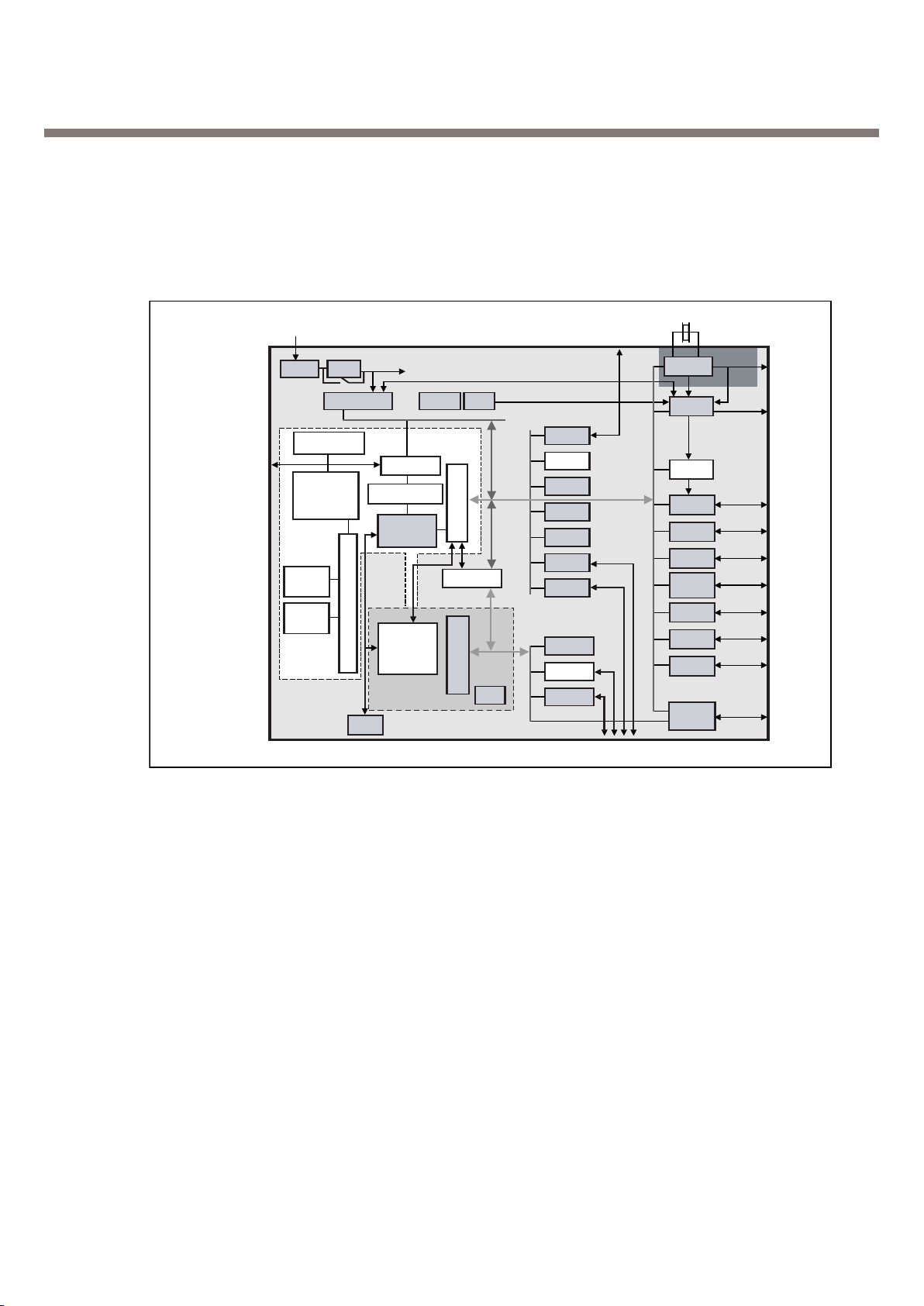
3.2. Digital Baseband(DBB) Processor
Figure 5. Top level block diagram of the Calypso lite
13 MHz
or 26 MHz TCXO
SLICER
External
ARM7
Momories
DIV-2
DPLL & CLKM
13MHz
WTDOG
INTH
MCU top-cdll
Boot Rom
Memory
Protect
U
nit
MEMIF
Debug Unit
ARM7
B
R
I
D
G
E
W
r
i
t
e
b
u
f
.
1 Mbit
SRAM
1 Mbit
SRAM
cDSP
S28C128
JTAG
DSP subchip
B
R
I
D
G
E
DMA (4+)
1NTH
RHEA bus
CRYPT
RIF
MCSI
uWIRE
ARMI
O
TIMER1
TIMER2
Die ID
RHEA bus
GEA
SPI
Asywchro mms WAKE_UP
ENABLE-CK13Mhz
CK 32Khs
32 Mhz CRYSTAL
TT
Alarm
RTC
ULPD
GSM time
TPU
TSP
SIM
PWL
UART
IRDA
PWT
LPG
12C
UART
modem
SK API
3. H/W Circuit Description
3.2.1. General Description
CALYPSO lite is a chip implementing the digital base-band processes of a GSM/GPRS mobile
phone.
This chip combines a DSP
Controller core with emulation facilities (ARM7TDMIE), internal 8Kb of Boot ROM memory, 2M bit
SRAM memory, a clock squarer cell, several compiled single-port or 2-ports RAM and CMOS gates.
The chip will fully support the Full-Rate, Enhanced Full-Rate and Half-Rate speech coding.
CALYPSO lite implements all features for the structural test of the logic (full-SCAN, BIST, PMT,
0JTAG boundary-SCAN).
sub-chip (LEAD2 CPU) with its program and data memories, a Micro- -
-
19
-

3. H/W Circuit Description
3.2.2. Block Description
CALYPSO lite architecture is based on two processor cores ARM7 and DSP using the generic RHEA
bus standard as interface with their associated application peripherals.
CALYPSO lite is composed from the following blocks:
• ARM7TDMIE : ARM7TDMI CPU core
• DSP subchip
• ARM peripherals:
General purpose peripherals
• ARM Memory Interface for external RAM, Flash or ROM
• 2 Mbit Static RAM with write-buffer
Application peripherals
• ARM General purposes I/O with keyboard interface and two PWM modulation signals
• UART 16C750 interface (UART_IRDA) with
- IRDA control capabilities (SIR)
- Software flow control (UART mode).
• UART 16C750 interface (UART_MODEM) with
- hardware flow protocol (DCD, CTS/RTS)
- autobaud function
• SIM Interface.
• TPU(Time Processing Unit) : Processing for GSM time base
• TSP(Time Serial Port) : GSM data interface with RF and ABB
* Calypso lite is internally 39MHz machine (25ns machine cycle), so it requires 3 wait-state for 80ns
access(25*4 = 100 ns).
-
20
-
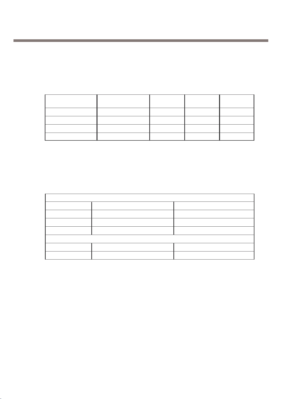
3.2.3. External Devices connected to memory interface
Table 3-2. Memory interface
Device Name MakerWrite Read
Access TimeAccess Time
FLASH 1
SRAM
LCD
Melody IC
TH50VPF5683CDSB
TH50VPF5683CDSB
RB187Z10A
YMU762
70ns
70ns
50ns
50ns
70ns
50ns
70ns
80ns
Toshiba
Toshiba
SII
Yamaha
Interface SPEC
TSP (Time Serial Port)
Resource Interconnection Description
TSPDO ABB & RF main Chip Control Data
TSPEN0 ABB ABB Control Data Enable Signal
TSPEN1 RF main Chip RF Control Data Enable Signal
TPU (Time Processing Unit) Parallel Port
TSPACT00 RESET_RF RF main Chip Reset Signal
TSPACT05 PA_ON Power Amp ON signal
Table 3-3. RF Interface Spec.
3.2.4. RF Interface (TPU, TSP block)
3. H/W Circuit Description
Calypso lite uses this interface to control Nausica_CS(ABB Processor) and Clara(RF Processor) with
GSM Time Base
3.2.5. SIM interface
SIM interface scheme is shown in (Figure 6). SIM_IO, SIM_CLK, SIM_RST ports are used to
communicate DBB with
ABB and the Charge Pump in
ABB enables 1.8V/3V SIM operation
SIM Interface
] SIM_CLK ------------- SIM card reference clock
] SIM_RST ------------- SIM card async/sync reset
] SIM_IO ---------------- SIM card bidirectional data line
] SIM_PWCTRL ------ SIM card power activation
] SIM_RnW ------------ SIM card data line direction
] SIM_CD -------------- SIM card presence detection
-
21
-
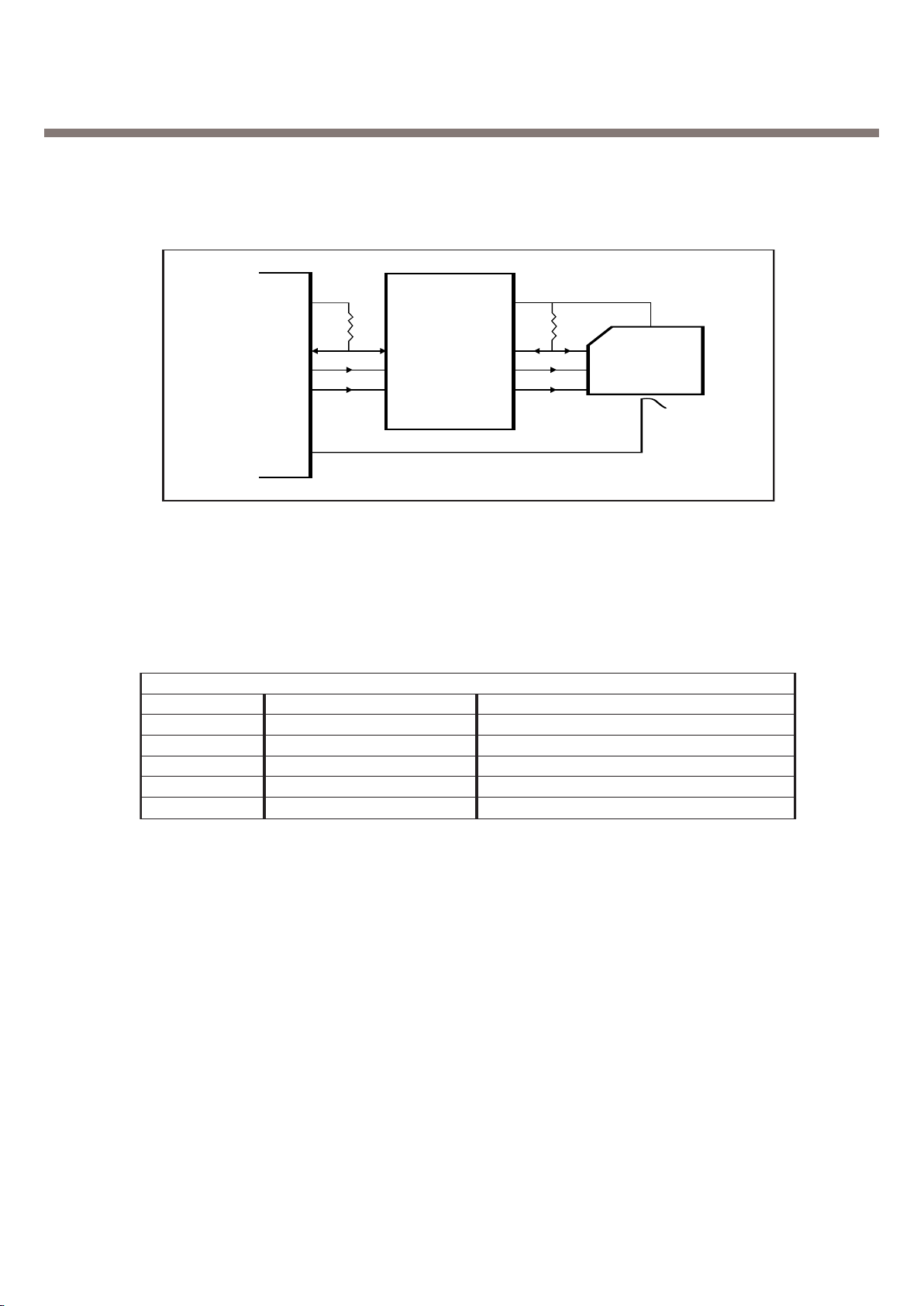
3. H/W Circuit Description
Fig
ure
6.
SIM
Int
erfa
ce
ABB
CARD
VDD
20K
20K
IO
CLK
RST
SIM_PWCTRL
SIM_IO
SIM_CLK
SIM-RST
SIM_CD
SVDO
SRST5
SIO5
SCLK5
SRST5
SIO5
SCLK5
Figure 3-4. UART Interface Spec.
UART MODEM(UART)
Resource Name Remark
TX_MODEM TXD Transmit Data
RX_MODEM RXD Receive Data
CTS_MODEM CTS ClearTo Sen d
RTS_MODEM RTS RequestTo
Sen
d
GPIO 3 DSR Data Set Ready
3.2.6. UART Interface
MG191 has two UART Drivers as follow :
- UART : Hardware Flow Control / Fax&Data Modem
-
22
-
I/O #
I/O (2)
I/O (3)
I/O (4)
I/O (5)
I/O #
LCD BACKLIGHT
MELODY IRQ
LED ON
DSR
NC
SIM PWCTRL
NC
LCD BACKLIGHT
LCD RESET
LCD BACKLIGHT
MIDI RESET
INLED R
INLED G
PCM SYNC
BHE
BLE
GPIO
GPIO
GPIO
GPIO
GPIO
GPIO
GPIO
GPIO
GPIO
GPIO
GPIO
GPIO
SIM
GPIO
MEMORY
HIGH
HIGH
LOW
HIGH
HIGH
LOW
HIGH
LOW
LOW
HIGH
HIGH
HIGH
LOW
LOW
LOW
HIGH
LOW
LOW
HIGH
LOW
HIGH
HIGH
LOW
LOW
HIGH
HIGH
I/O (6)
I/O (7)
I/O (8)
I/O (9)
I/O (11)
I/O (12)
I/O (13)
I/O (14)
I/O (15)
I/O (10)
I
O
I
O
I
O
O
O
O
O
O
I
O
O
O
(Open) (Closed)
I/O # I/OApplication
Resource
State
Inactive
State
Active
State
Table 3-5. GPIO Map Table
3. H/W Circuit Description
3.2.7. GPIO map
In total 16 allowable resources, MG191 is using 13 resources except 3 resources dedicated to SIM
and Memory. MG191 GPIO(General Purpose Input/Output) Map, describing application, I/O state,
and enable level, is shown in below table.
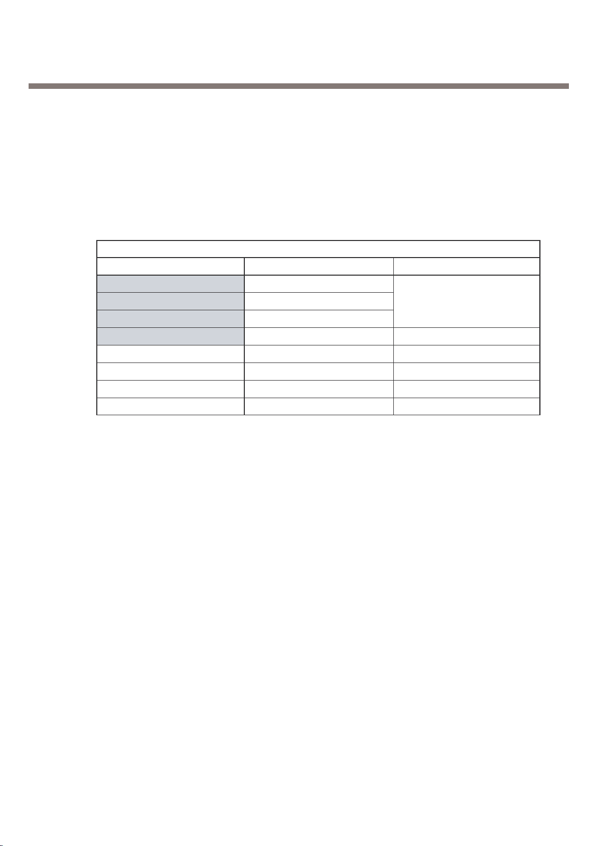
3.3. Analog Baseband(ABB) Processor
3.3.1. General Description
IOTA is Analog Baseband (ABB)Chip supports GSM900, DCS1800, PCS, GPRS Class 10 with Digital
Basband Chip(Calypso G2).
IOTA processes GSM modulation/demodulation and power management operations.
Block Description
Audio Signal Processing & Interface
-
- Baseband in-phase(I), quadrature(Q) Signal Processing
- RF interface with DBB (time serial port)
- Supply voltage regulation
- Battery charging control
- Switch ON/OFF
- 1.8V/3V SIM card Interface
- 4 internal & 4external ADC channels
-
23
-

3. H/W Circuit Description
Figure 7. Audio Interace Block Diagram
HSMICP
10 dB
SLR = (8 dB + 3 dB)
AUXI
4.6 dB or
28.2 dB
MICAMP
25.6 dB
STMR = (13 dB + 5 dB)
AUXAMP
-5 dB
HSOAMP
-5 dB
DAC and
Smoothing
Filter 0 dB
Digital
Modulator
0 dB
PGA
Gain : 0 dB
-6 dB to 6 dB
1-dB Step
DL Filter
0 dB
Volume
Control
0 dB to - 24 dB
+ Mute
3 dBm0
Full Scale
16 Bits
ADC
2.48 dB
VREF 1.75V
UL Filter
3.25 dB
PGA :
Gain : 0dB
12 dB to - 12 dB
1-dB Step
3 dBm0
Full Scale
16 Bits
1b + 1b
620 mV
RMS
365 mV
RMS
78 mV
RMS
Sensitivity
-49.3 dBv/Pa
Sensitivity
106.7 dBspl/Vrm
RLR = (2 dB + 3 dB)
32.5 mV
RMS
1.385 V
RMS
1.237 V
RMS
692 mV
RMS
346 mV
RMS
EARAMP
1 dB
Sidetone :
1 dB to - 23 dB
Mute
3.3.2. Audio Signal Processing & Interface
Audio signal processing is divided Uplink path and downlink path.
The uplink path amplifies the audio signal from MIC and converts this analog signal to digital signal
and then transmit it to DBB Chip. This transmitted signal is reformed to fit in GSM Frame format and
delivered to RF Chip.
MICBIAS is 2.0V level. The downlink path amplifies the signal from DBB chip and outputs it to
Receiver(or Speaker).
-
24
-
3. H/W Circuit Description
Figure 8. Baseband codec Block Diagram
Output Voltage Usage
VRDBB 1.5V Digital Core of DBB
VRI O 2.8V Peripheraldevices
VRM EM 2.8V External memor y
VRRAM 2.8V LCD & peripheral devices
VRABB 2.8V Analog Block of ABB
VRSIM 2.85 SIM card driver
VRRTC 1.5V RTC & 32kHz-crystal
From TSP
From BSP
Burst
Buffer 1
Timing
Control
GMSK
Modulator
6-Bit
DAC
Off
set
Register
Offset
Register
Low-Pass
Filter
Low-Pass
Filter
BULQM
BULQP
BULIM
BULIP
16 270 kHz
6-Bit
DAC
Burst
Buffer 2
270 kHz
Cosine
Ta b
le
Sine
Ta ble
10-Bit
DAC
10-Bit
DAC
3.3.3. Baseband Codec (BBC)
Baseband codec is composed of baseband uplink path(BUL) and baseband downlink path(BDL).
BUL makes GMSK(Gaussian Minimum Shift Keying) modulated signal which has In-phase(I) component and quadrature(Q) component with burst data from DBB. This modulated signal is transmitted
through RF section via air.
BDL process is opposite procedure of BUL. Namely, it performs GMSK demodulation with input
analog I&Q signal from RF section, and then transmit it to DSP of DBB chip with 270.833kHz data
rate through BSP.
-
25
-

Figure 9. Power Supply Scheme
VBAT
ABB
DBB split power
SL
SL
SL
SL
SL
NM
VCMEM
VIMEM
VCDBB
VCIO1
VCIO2
VCABB
VBAT
VBACKUP
BBS
ABB
VRPC core
BACKUP
VCRAM
VRSIM
VRRAM
VRMEM
VDDS-MIF
VLRTC
VLRTC
VLRTC
VDD-RTC
VDDS-RTC
VDD
VDDPLL
VDDS1
VDDS2
VSDBB
VRDBB
VRIO1
VRIO2
VRABB
UPR
Power split domain
RSIM
1.8/2.9V
10 mA
SIM CARD
Ext SRAM
FLASH
MEMORY
INTERFACE,
All ASIC modules,
ARM7,
LMM,
Internal SRAM
PLL
IOTA I/O,
RF I/O
13 MHz_IN
13 MHz_Out
RTC
XO32K
(IT WAKEUP,
nRESPWONZ,
ON nOFF)
RRAM
1.8/2.8V
50 mA
RMEM
1.8/2.8V
60 mA
RDBB
1.18/1.4/1.8V
120 mA
RIO
2.8V
100 mA
ABB
Digital
core io
ABB
Analog core
RABB
2.8V
80 mA
RRTC
1.18/1.4/1.8V
10 uA
1uF
4.7u
F
4.7uF
10uF
10uF
2.2uF
1uF
1uF
Sel
2.8V
Sel 1.4V
Sel 1.8V
Sel 1.8V
BK
SL
SLP
ML
: regulators ON in BACKUP / SLEEP / NORMAL mode
: rggulators ON in SLEEP / NORMAL mode
: idem SL + reverse current protection
: regulators ON in NORMAL mode
: reserved for ABB private use only
3. H/W Circuit Description
3.3.4. Voltage Regulation (VREG)
There are 7 LDO(Low Drop Output) regulators in ABB chip.
The output of these 7 LDOs are as following table. (Figure 9) shows the power supply related locks
of DBB/ABB and their interfaces in MG191.
-
-
26
3. H/W Circuit Description
ADC 8 channels
Resource NameDescription
VCHG VCHG
VBAT VBAT Charging Management
ICHG ICHG
VBACKUP VBACKUP Backup Battery
ADIN1 JACK_DETECT Jack plug-in detect
ADIN2 BATT_TEMP Battery Detect
ADIN3 TEMPSENSE Temperature Sensing
ADIN4 HOOK_DETECT HOOK_DETECT
Table 3-6. ADC Channel Spec.
3.3.5. ADC Channels
ABB ADC block is composed of 4 internal ADC(Analog to Digital Converter) channels and 4 external
ADC channel. This block operates charging process and other related process by reading battery
voltage and other analog values.
-
27
-
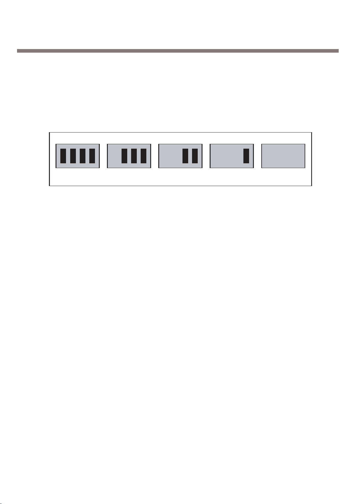
4.2V-3.93V
3.92V-3.79V
3.78V-3.72V
3.71V-3.62V
3.61V-3.50V
Figure 10. Battery Block Indication
3. H/W Circuit Description
3.3.6. Charging
Charging block in ABB processes charging operation by using VBAT, ICHG value through ADC
channel. Battery Block Indication and SPEC of MG191 is as follow.
1. Charging method : CC-CV
2. Charger detect voltage : 4.2V
3. Charging time : 2h30min
4. Icon stop current : 100mA
5. Charging current : 500mA
6. CV voltage : 4.2V
7. Cutoff current : 50mA
8. Full charge indication current (icon stop current) : 100mA
9. Recharge voltage : 4.05V
10. Low battery alarm
a. Idle : 3.64V
b. Dedicated : 3.50V
1. Low battery alarm interval :
1
a. Idle : 3min
b. Dedicated:1min
12. Switch-off voltage : 3.35V
13. Charging temperature adc range
a. ~ -2°C : not charging operation.
C : charging.
°
C ~ 47
°
b. -2
c. 47°C~ : not charging operation.
-
28
-
3. H/W Circuit Description
No. Pin Name Function
1 Main_CS
2 LCD_RESET
3 A(0)
4WR
5RD
6 D(0)
7 D(1)
8 D(2)
9 D(3)
LCD Chip set
LCD Reset
Address Line
LCD Write Control
LCD Read Control
Date input
Date input
Date input
Date input
Table 3-7. LCD FPC Interface Spec.
3.3.7. Switch ON/OFF
MG191 Power State : Defined 4cases as follow
] Power-ON : mobile is powered by main battery or backup battery.
] Power-OFF : mobile isn’t any battery.
] Switch-ON : mobileis powered and waken up from switch-off state.
] Switch-OFF : mobile is powered to maintain only the permanent function(ULPD).
To enter into Switch-ON state, one of followinf 4 condition is satisfied.
] PWR-ON pushed after a debouncing time of 30ms.
] ON_REMOTE : After debouncing, when a falling edgeis detected on RPWON pin.
] IT_WAKE_UP : When a rising edge is detected on RTC_ALARM pin.
] CHARGER_IC : When a charger voltage is above VBAT+0.4V on VCHG.
3.3.8. Memory
MG191a using 64Mbit Flash + 32Mbit SRAM with 16 bit parallel data bus thru ADD01 ~ ADD22.
3.3.9. Display & FPCB Interface
LCD module include :
Main LCD: 120*64 Mono Scale LCD
Main LCD Backlight : EL-Backlight
LCD module is connected to main board with 26 pin FPCB and connected to Speaker, Receiver,
Vibrator.
-
29
-
 Loading...