

LG MG185C Service Manual

Date: May, 2006 / Issue 1.0
Service Manual
MG185c
ABC
GHI
PQRS
JKL
TUV
WXYZ
MNO
DEF
DIGITAL IMAGE ENHANCER
Service Manual
Model : MG185c

- 3 -
1. INTRODUCTION ...............................5
1.1 Purpose .................................................. 5
1.2 Regulatory Information............................ 5
2. PERFORMANCE...............................7
2.1 Product Name ..........................................7
2.2 Supporting Standard................................7
2.3 Main Parts : GSM Solution.......................7
2.4 HW Features............................................8
2.5 S/W Features ...........................................9
3. TECHNICAL BRIEF.........................11
3.1 Baseband Part Technical Brief ..............11
3.1.1 BaseBand Components
(Component Side) ................................11
3.1.2 BaseBand Components (Keypad Side)12
3.1.3 Digital Baseband(DBB) Processor .......13
3.1.4 Analog Main Processor (ABB)..............14
3.1.5 Memory ................................................15
3.1.6 Voltage Regulation (LDO) ....................16
3.1.7 MIDI......................................................17
3.1.8 Charging...............................................18
3.1.9 KEY Back-light Illumination ..................19
3.1.10 CAMERA Interface.............................19
3.1.11 SIM.................................................... 20
3.1.12 Keypad ...............................................21
3.2 RF Part Technical Brief..........................22
3.2.1 RF Part components ............................22
3.2.2 Tx / Rx Part Description .......................23
3.2.3 Receiver Part Description.....................24
3.2.4 Transmitter Part Description.................29
4. TROUBLESHOOTING ....................32
4.1 BaseBand Part Troubleshooting............32
4.2 RF Part Troubleshooting........................65
4.3 TX Part Trouble Shooting ......................70
5. DOWNLOAD ...................................74
5.1 H/W Tool Setup......................................74
5.2 Install & Directory structure....................75
5.3 Configuration setting ..............................76
5.4 Download sequence ..............................79
6. BLOCK DIAGRAM..........................80
6.1 The Block Diagram of the
Baseband Part .......................................80
6.2 The Block Diagram of the RF Part .........81
7. Circuit Diagram ..............................83
8. pcb layout.......................................89
9. Calibration ......................................91
9.1 H/W Tool Setup......................................91
9.2 Test Jig Operation..................................92
9.3 Install & Directory structure....................94
9.4 Others Directory structure of CM_GSM .95
9.5 Cal. Procedure .......................................96
9.6 Cal. sequence ........................................97
10. EXPLODED VIEW &
REPLACEMENT PART LIST ....... 99
10.1 Exploded View .................................... 99
10.2 Replacement Parts ............................101
10.3 Accessory ......................................... 116
Table Of Contents

- 4 -

1. INTRODUCTION
- 5 -
1.1 Purpose
This manual provides the information necessary to repair, calibration, description and download the
features of this model.
1.2 Regulatory Information
A. Security
Toll fraud, the unauthorized use of telecommunications system by an unauthorized part (for example,
persons other than your company’s employees, agents, subcontractors, or person working on your
company’s behalf) can result in substantial additional charges for your telecommunications services.
System users are responsible for the security of own system. There are may be risks of toll fraud
associated with your telecommunications system. System users are responsible for programming and
configuring the equipment to prevent unauthorized use. The manufacturer does not warrant that this
product is immune from the above case but will prevent unauthorized use of common-carrier
telecommunication service of facilities accessed through or connected to it.
The manufacturer will not be responsible for any charges that result from such unauthorized use.
B. Incidence of Harm
If a telephone company determines that the equipment provided to customer is faulty and possibly
causing harm or interruption in service to the telephone network, it should disconnect telephone
service until repair can be done. A telephone company may temporarily disconnect service as long as
repair is not done.
C. Changes in Service
A local telephone company may make changes in its communications facilities or procedure. If these
changes could reasonably be expected to affect the use of the this phone or compatibility with the
network, the telephone company is required to give advanced written notice to the user, allowing the
user to take appropriate steps to maintain telephone service.
D. Maintenance Limitations
Maintenance limitations on this model must be performed only by the manufacturer or its authorized
agent. The user may not make any changes and/or repairs expect as specifically noted in this manual.
Therefore, note that unauthorized alternations or repair may affect the regulatory status of the system
and may void any remaining warranty.
1. INTRODUCTION

1. INTRODUCTION
- 6 -
E. Notice of Radiated Emissions
This model complies with rules regarding radiation and radio frequency emission as defined by local
regulatory agencies. In accordance with these agencies, you may be required to provide information
such as the following to the end user.
F. Pictures
The pictures in this manual are for illustrative purposes only; your actual hardware may look slightly
different.
G. Interference and Attenuation
Phone may interfere with sensitive laboratory equipment, medical equipment, etc.Interference from
unsuppressed engines or electric motors may cause problems.
H. Electrostatic Sensitive Devices
ATTENTION
Boards, which contain Electrostatic Sensitive Device (ESD), are indicated by the sign.
Following information is ESD handling:
• Service personnel should ground themselves by using a wrist strap when exchange system boards.
• When repairs are made to a system board, they should spread the floor with anti-static mat which is
also grounded.
• Use a suitable, grounded soldering iron.
• Keep sensitive parts in these protective packages until these are used.
• When returning system boards or parts like EEPROM to the factory, use the protective package as
described.
2. PERFORMANCE
- 7 -
2.1 Product Name
MG185C : GPRS Class 10
2.2 Supporting Standard
2.3 Main Parts : GSM Solution
2. PERFORMANCE
Item Feature Comment
900/1800/1900
Tri-Band (900/1800/1900)
Supporting Standard
with seamless handover
Phase 2+(include AMR)
SIM Toolkit : Class 1,2,3,A~E
GSM900 TX : 880 - 915 MHz
GSM900 RX : 925 - 960 MHz
Frequency Range
DCS1800 TX : 1710 - 1785 MHz
DCS1800 RX : 1805 - 1880 MHz
PCS1900 TX : 1850 - 1910 MHz
PCS1900 RX : 1930 - 1990 MHz
WAP 2.0
Application Standard
JAVA 2.0
Digital Baseband Calypso-AMR C035(D751992GHH)
Analog Baseband IOTA(TWL3025)
RF Chip Aero2(SI4210-GM)

- 8 -
2.4 HW Features
Item Feature Comment
Form Factor Bar Type with camera
1) Capacity
Battery
Standard :
Li-Ion, min 830mAh (LGC)
2) Packing Type : Inner Pack
Size Standard : 103.9 X 45.6 X 15.8 mm
Weight 85 g
Volume TBD
PCB One PCB:8 Layers , 1t
Stand by time 200 hrs DRX6
Charging time 3 hrs
Min : about 2.5 hrs
GSM 900MHz
Talk time
Min : about 3.0 hrs
DCS 1800MHz
PCS 1900MHz
GSM 900 : -108 dBm
RX sensitivity DCS 1800 : -107dBm
PCS 1900 : -107 dBm
GSM 900 : 33 dBm Class4 (GSM)
TX output power DCS 1800 : 30dBm
PCS 1900 : 30 dBm Class1 (PCS)
GPRS compatibility GPRS Class 10
SIM card type Plug-In SIM 3V
65K Color STN (128 X 128)
Display
Backlight : White LED
Status Indicator Indicator LED
Alphanumeric Key : 10 0 ~ 9
Keypad
Function Key : 6 Nevi. Key, Soft key, etc
Side Key : 1 camera
Total # of Keys : 22 SND, END/PWR, CLR
ANT Intenna
System connector 24 Pin
Ear Phone Jack 3 Pole (2.5mm)
PC synchronization Yes
Memory
Flash : 128 Mbit Spansion
SRAM : 64 Mbit
Speech coding FR, EFR, HR, AMR
Data & Fax Built in Data & Fax support
Vibrator Built in Vibrator
MIDI(for Buzzer Function) YAMAHA 40Poly
Voice Recording Yes
Speaker Phone Yes
Travel Adapter Yes
CDROM TBD
Options
Ear-Microphone
Data Cable

- 9 -
2.5 S/W Features
Item Feature Comment
RSSI 0 ~ 5 Levels
Battery Charging 0 ~ 4 Levels
Key Volume 0 ~ 5 Level
Audio Volume 1 ~ 5 Level
Time / Date Display Yes NITZ
Multi-Language Yes English / Spanish / France
Quick Access Mode Phone Book / My MEdia / Message /
Java or SIM Toolkit
PC Sync Schedule / Phonebook / MEMO / Photo
Speed Dial Yes (2~9) Voice mail center -> 1 key
CLIP / CLIR Yes (different melody)
Speaker Phone Yes
Phone Book 3 Numbers + 1 Memo + 1 e-mail + Total 255 Member
Group Select + Picture
Last Dial Number Yes (20)
Last Received Number Yes (20)
Last Missed Number Yes (10)
Search by Number / Name Name only
Group 7 Possible Rename
Fixed Dial Number Yes
Service Dial Number Yes
Own Number Yes
Voice Memo Yes
Call Reminder Yes
Network Selection Automatic / Manual
Mute Yes
Call Divert Yes
Call Barring Yes
Call Charge (AoC) No
Call Duration Yes
SMS (EMS) 100 EMS : Release4
(Except Text align)
E-Mail Yes Over SMS
SMS Over GPRS Yes
EMS Melody / Picture Yes
Send / Receive / Save
Long Message MAX 918 Characters
Cell Broadcast Yes
Download Over the WAP
Game Yes TBD
Calendar Yes
Memo 20

2. PERFORMANCE
- 10 -
- Some features depend on requirement.
World Clock Yes
Unit Convert Length/Surface/Volume/Weight
Tip Calculator Yes
Fax & Data Yes
Wall Paper Yes Default 5ea
WAP Browser Over WAP 2.0 w/o HTTP UP Brower 6.2.3
Download Melody /
Yes Over WAP
Wallpaper
SIM Lock Yes Operator Dependent
SIM Toolkit Class 1, 2, 3, A-E
MMS Yes Openwave MMS Client
EONS Yes
CPHS Yes V4.2
ENS Yes
Camera Yes VGA CMOS, Digital 4x
JAVA Yes
CLDC V1.1 / MIDP V2.0
Download Over WAP
Voice Dial Yes
IrDA NO
GPRS Yes Class10
Hold / Retrieve Yes
Conference Call Yes Max. 6
DTMF Yes
Memo pad Yes Yes
TTY NO
AMR Yes
3. TECHNICAL BRIEF
- 11 -
3.1 Baseband Part Technical Brief
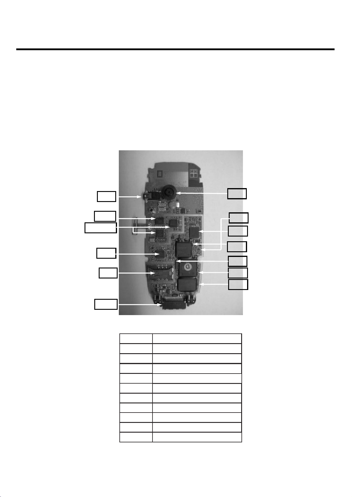
3.1.1 BaseBand Components (Component Side)
3. TECHNICAL BRIEF
U102
X101
U101
J201
CN301
U501,U502
U202
J401
U201
U401
U602
FL501
S601
Analog Baseband Chipset (IOTA)
Digital Baseband Chipset (Calypso)
Crystal (32.768KHz Oscillator)
Melody IC (40 Poly)
Memory (128M Flash x 64M pSRAM)
EAR Jack
SIM Connector
Analog Switch (Single)
U101
U102
X101
U201
U401
J201
J401
U202
U501,U502 RF
IO ConnectorCN301
Camera ConnectorS601
3. TECHNICAL BRIEF
- 12 -
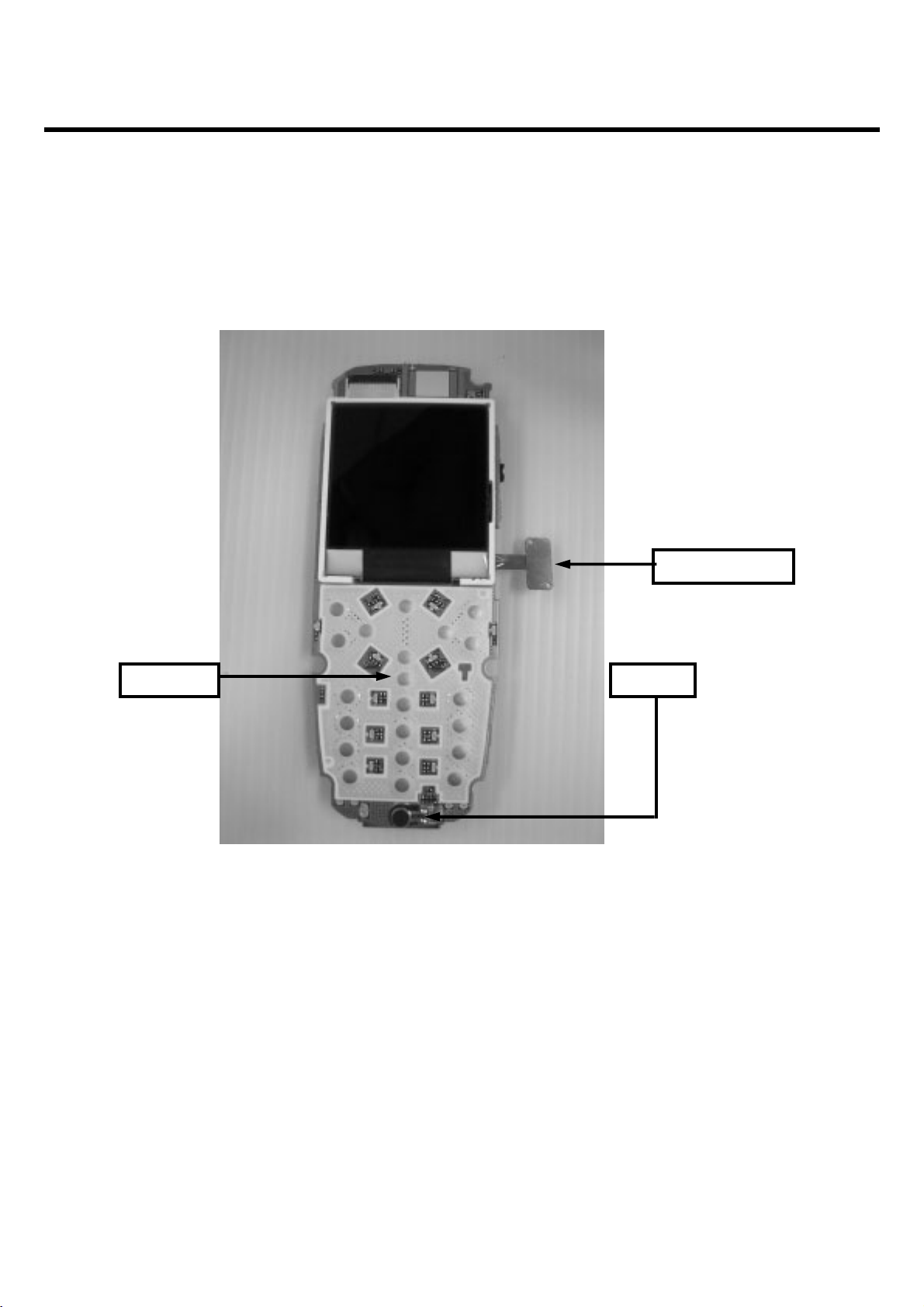
3.1.2 BaseBand Components (Keypad Side)
Dome key
Camera hot key
MIC201
3. TECHNICAL BRIEF
- 13 -
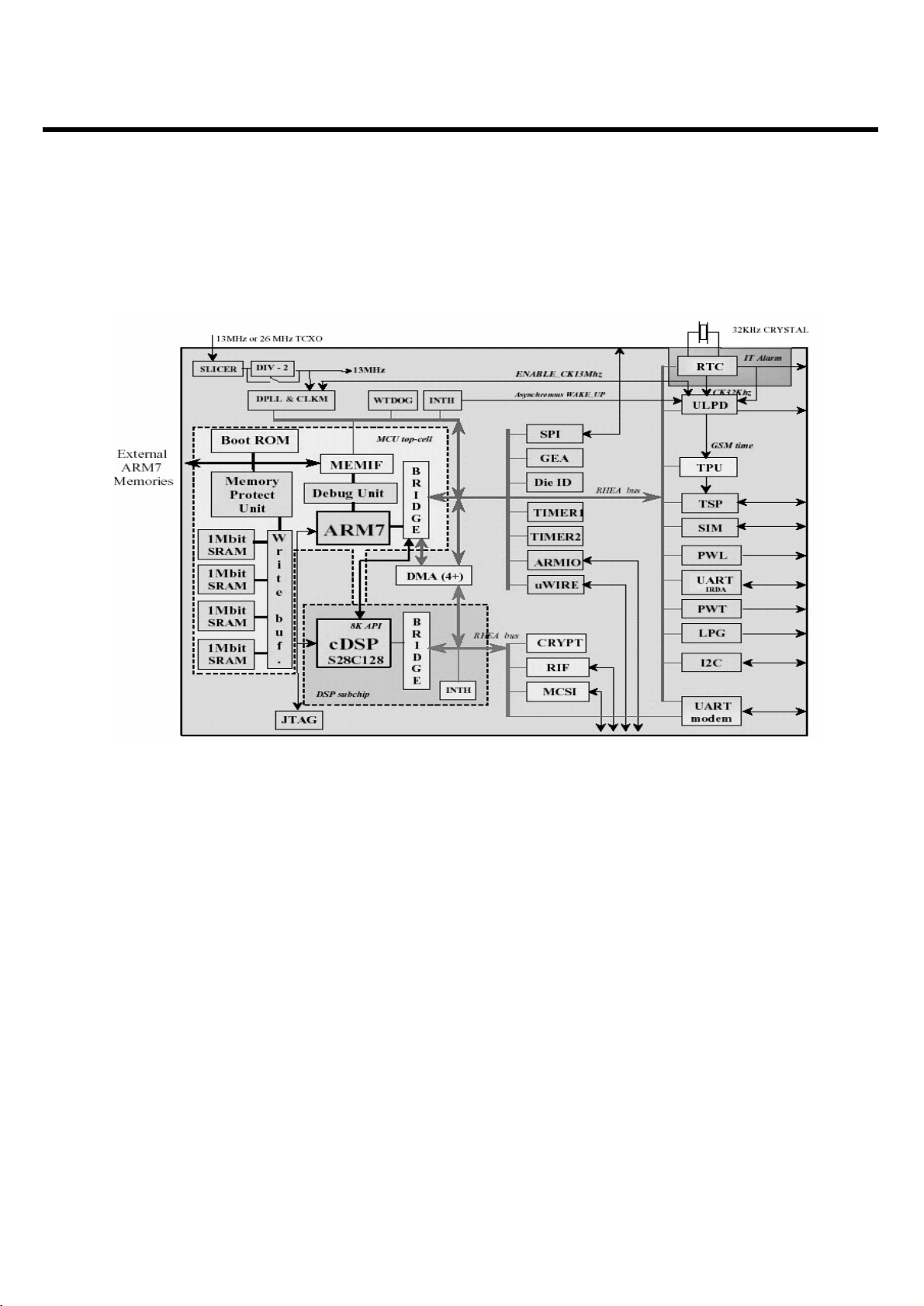
3.1.3 Digital Baseband(DBB) Processor
The Internal Architecture of the Calypso G2(HERCROM400G2)

3. TECHNICAL BRIEF
- 14 -
3.1.4 Analog Main Processor (ABB)
➢
Applications include GSM 850, 900, DCS 1800, PCS 1900 Cellular Telephones
➢
Voice Coder/Decoder (CODEC)
➢
Baseband CODEC single and multislot with I/Q RF Interface
➢
Auxiliary RF Converters
➢
SIM Card Interface
➢
Li-Ion or Ni-MH Battery Charging Control
➢
Six Low-DropOut, Low-Noise, Linear Voltage Regulators
➢
Dedicated Low Quiescent Current Mode on Regulators
➢
Voltage Detectors (with Power-Off Delays)
➢
Four Channel Analog-to-Digital Converters (ADC)
➢
Dedicated very low quiescent current domain supply
Figure 3-1. TWL3014 Functional Block Diagram
3. TECHNICAL BRIEF
- 15 -
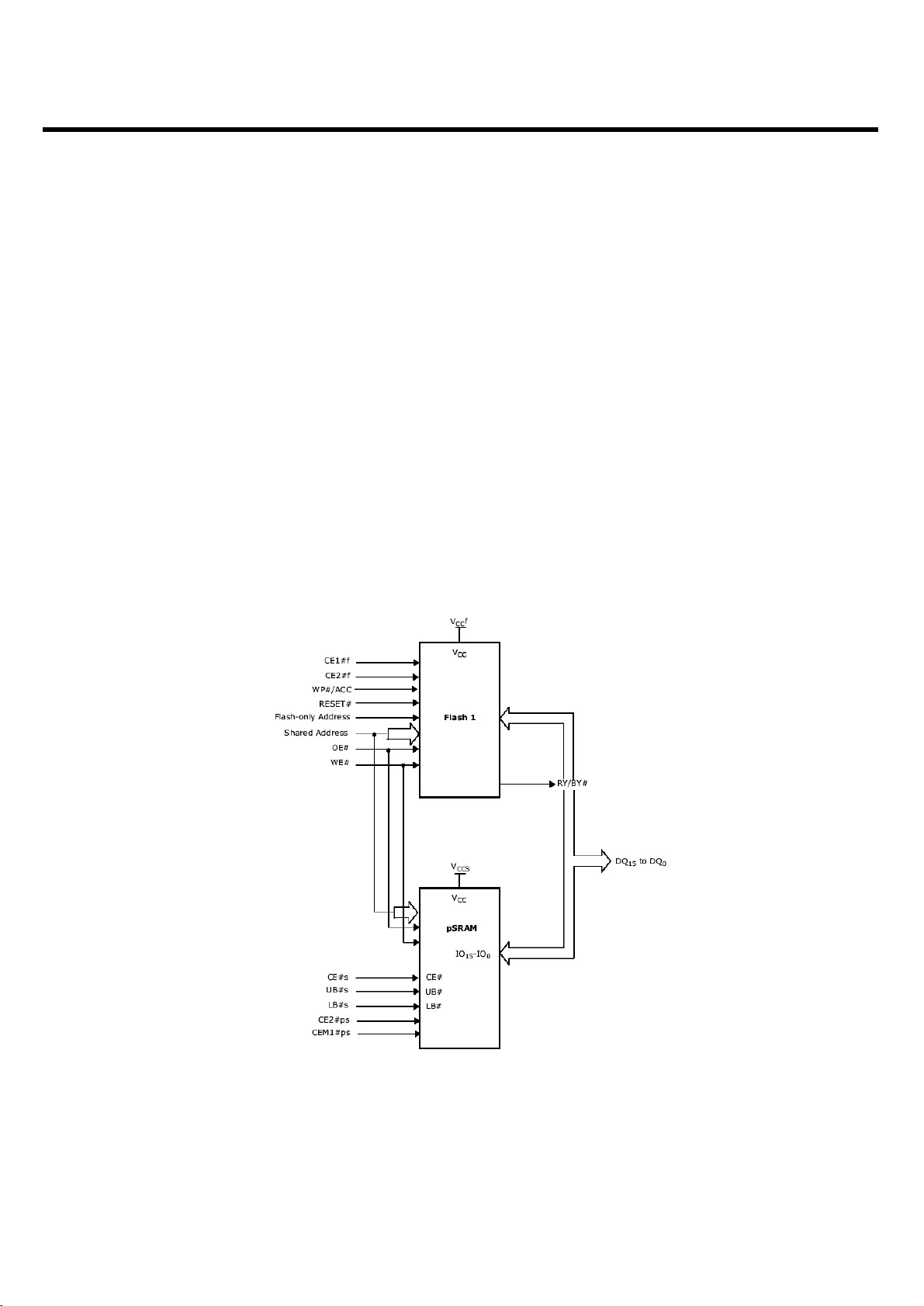
3.1.5 Memory
➢
Memory used MG185 is designed by SPANSION
➢
Mixed Multi-Chip Package containing a 64M pSRAM and 128M Flash Memory
➢
MCP(Multi-Chip Package) Features
•
Power Supply Voltage of 2.7 to 3.1 V
•
Operating Temperature of -25˚C to 85˚C
➢
pSRAM Features
•
Organization : 4 M x 16 bits
•
Power Dissipation : 50mA max.(Operating), 100µA max.(Standby)
➢
Flash Memory Features
•
Organization : 8M x 16 bits
•
Power Consumption
- 55 mA (Read operation)
- 10uA in standby or automatic sleep mode
Block Diagram
3. TECHNICAL BRIEF
- 16 -
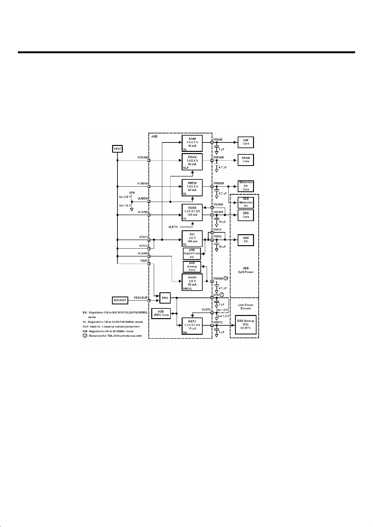
3.1.6 Voltage Regulation (LDO)
➢
V_DBB
•
Provides the power to the DBB(Calypso) Core
•
1.5V / 120mA max.
➢
V_RAM
•
Provides the power to the IC, MIDI, LCD, etc
•
2.8V / 50mA
➢
V_MEM
•
2.8V / 60mA max.
➢
V_ABB
•
Provides the power to the ABB(IOTA) Core
•
2.8V / 50mA max.
➢
V_IO
•
Provides the power to the Analog
S/W,Memory, etc
•
2.8V / 100mA max.
➢
V_RTC
•
Provides the power to the oscillator
•
1.5V / 30uA max.
➢
V_SIM
•
Provides the power to the SIM card
•
2.85V / 10mA max.
3. TECHNICAL BRIEF
- 17 -
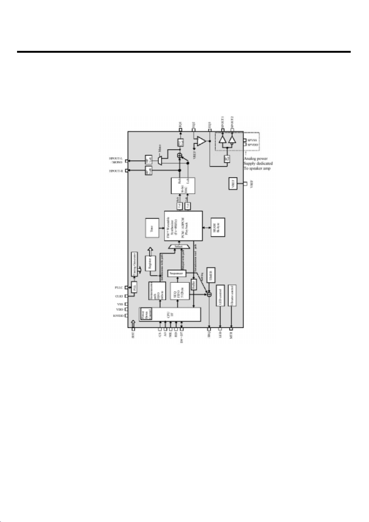
3.1.7 MIDI
➢
The ringing source of MG185 is the MIDI.
➢
The MIDI chip which is used in MG185 is YMU762 from YAMAHA.
➢
YMU762 generates 40-poly MIDI sound.

3. TECHNICAL BRIEF
- 18 -
3.1.8 Charging
➢
Charging method : CC-CV
➢
Charger detect voltage : 4.0V
➢
Charging time : about 2h
➢
Icon stop current : 100mA
➢
Charging current : 420mA
➢
CV voltage : 4.2V
➢
Cutoff current : 45mA
➢
Low battery alarm
•
Idle : 3.62V
•
Dedicated : 3.50V
➢
Switch-off voltage : 3.35V
➢
Charging temperature ADC range
•
~ -5˚C : not charging operation.
•
-5˚C ~ 50˚C : charging.
•
50˚C ~ : not charging operation.
4.2V ~ 3.92V 3.91V ~ 3.79V 3.78V ~ 3.72V 3.71V ~ 3.66V 3.65V ~ 3.35V
3. TECHNICAL BRIEF
- 19 -
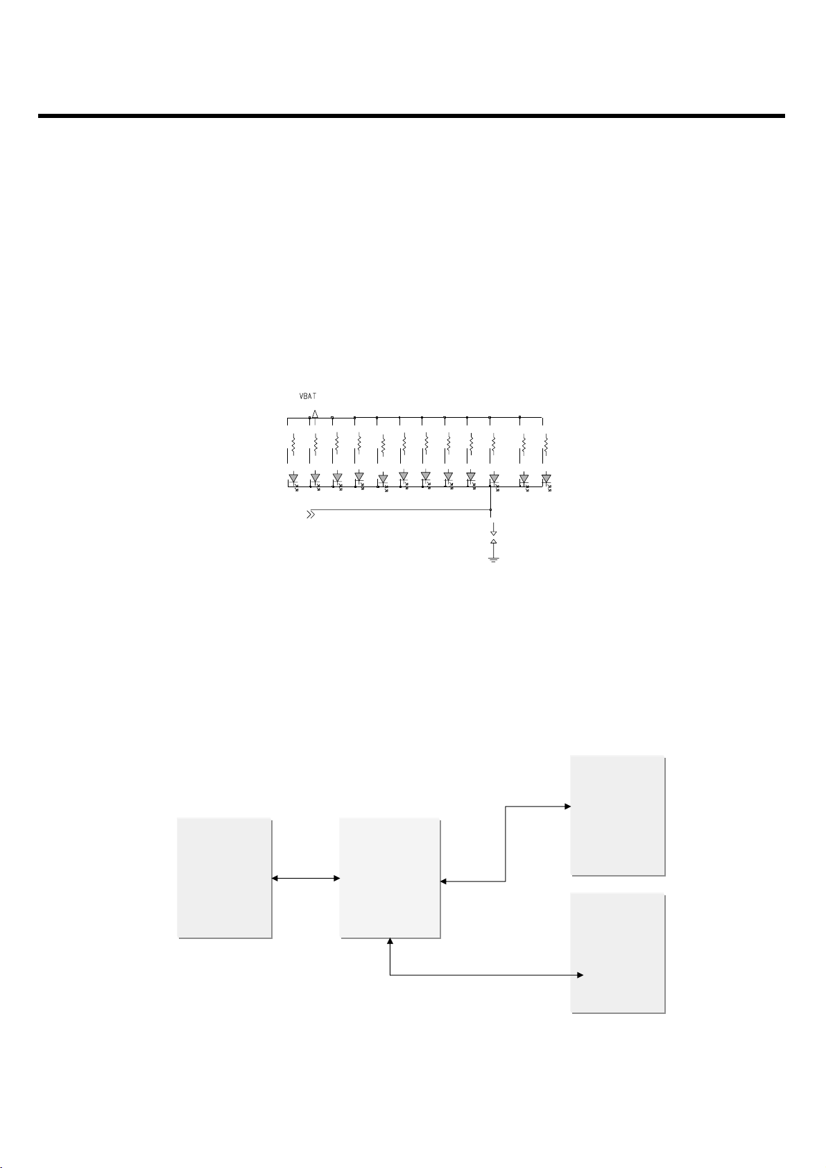
3.1.9 KEY Back-light Illumination (1)
➢
KEYPAD Back-light Scheme(slide part).
•
There are 12 Deep Blue LEDs in slide Board for ‘Number-key’.
•
Keypad Back-light is driven by ‘LEDB’ line from IOTA .
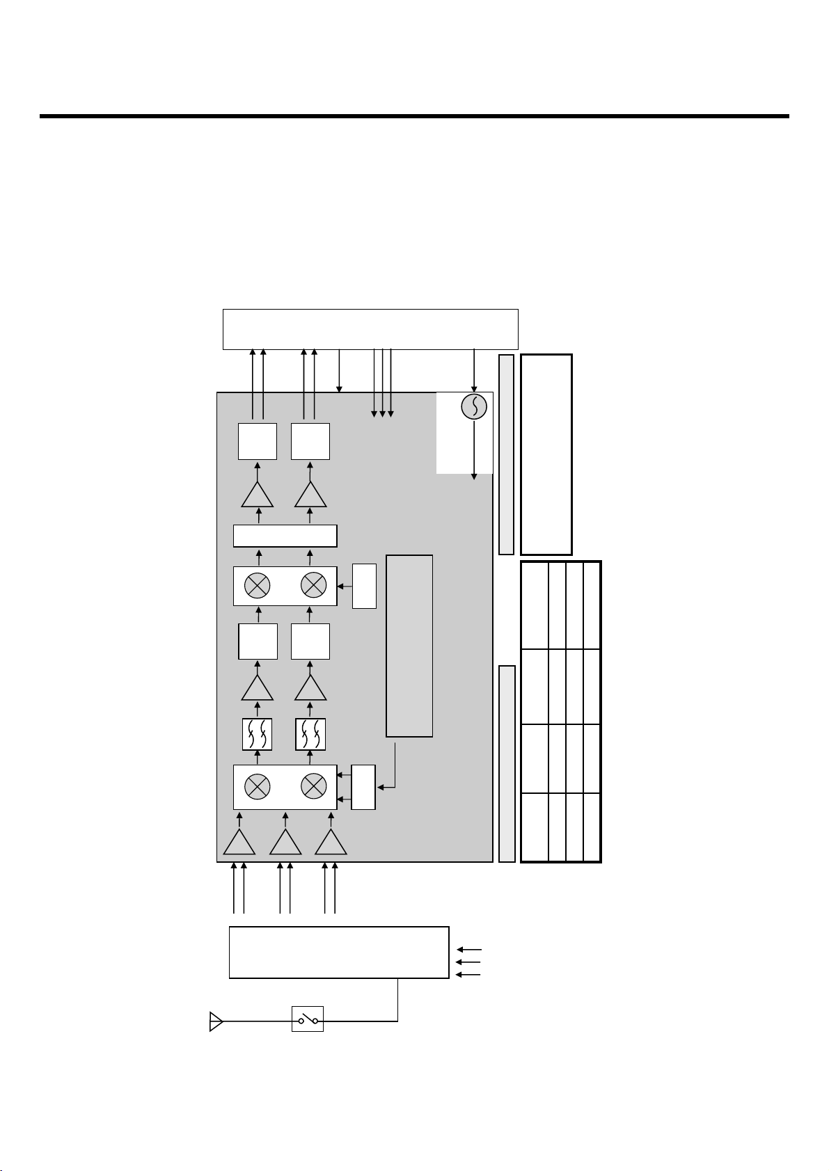
3.1.10 CAMERA Interface.
Allows you to use the built-in camera to take photos with the phone.
- The phone encodes up to 640 x 480 size with free size support
KEY Backlight
Built-in Camera BLOCK DIAGRAM
300
R303
300
LD302
R304
300
LD303
R305
LD304
300
R302
LEBB-S14H
LEBB-S14H
LD301
R306
300
LD305
R307
300
LD306
R308
300
LD307
R309
300
LD308
KEY BACKLIGHT
300
300
R311
R310
LD309
R351
LD310
300
300
R352
LD312
LD311
LEDB
SP301
CL761A
DBB
Camera IC
Main LCD
Camera
Sensor
3. TECHNICAL BRIEF
- 20 -
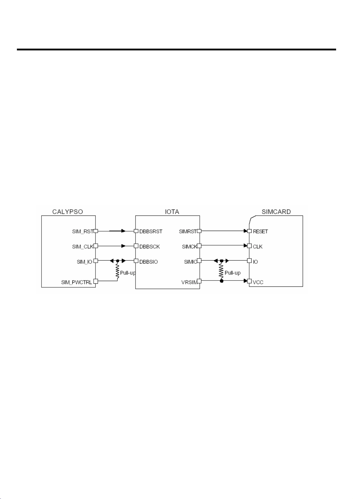
3.1.11 SIM
➢
SIM Interface
The Sim Card digital interface in ABB insures the translation of logic levels between DBB and Sim
Card, for the transmission of 3 different signals:
•
A clock derived from a clock elaborated in DBB, to the Sim-Card (DBBSCK -> SIM_CK)
•
A reset signal from DBB to the Sim Card (DBBSRST -> SIM_RST),
•
A serial data from DBB to the Sim Card (DBBSIO -> SIM_IO) and vice-versa.
The SIM card interface can be programmed to drive a 3V Sim Card.
SIM Card connection scheme
3. TECHNICAL BRIEF
- 21 -
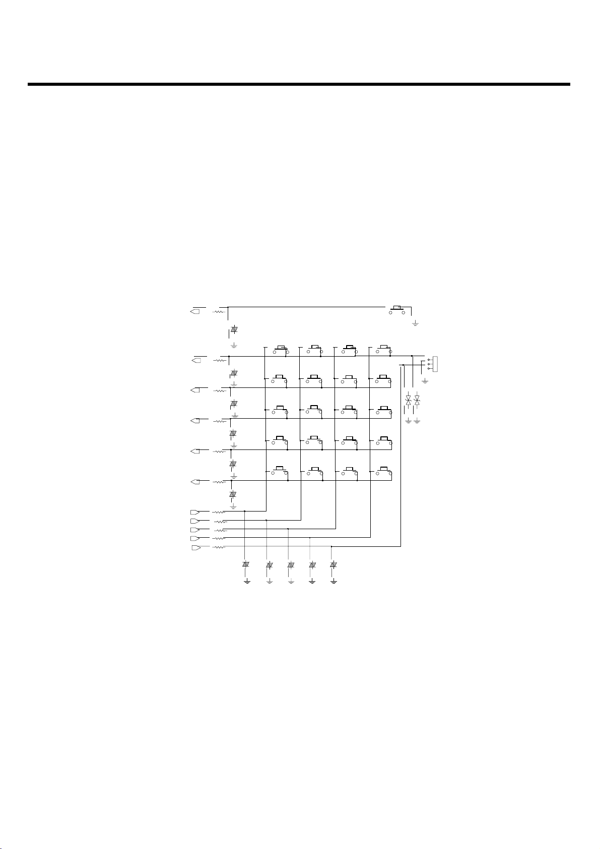
3.1.12 Keypad (1)
➢
KEYPAD Scanning Scheme (number -key).
The power key is connected to Calypso(DBB) directly using ‘PWON’.
The other number-key and navigation-key is connected to Calypso(DBB) using:
- KBR (4:0) input pins for row lines
- KBC (4:0) output pins for column lines
Keypad Scanning Scheme
PWON
KBR(1)
KBR(2)
KBR(3)
KBR(4)
KBR(0)
KBC(0)
KBC(1)
KBC(2)
KBC(3)
KBC(4)
R301
680
EVL5M02200
VA301
EVL5M02200
VA302
R315 680
EVL5M02200
VA303
EVL5M02200
VA304
R317 680
EVL5M02200
VA305
EVL5M02200
VA306
R319 680
R320 680
R322 680
680R312
680R316
680R318
680R321
680R323
EVL5M02200
KB302
12
KB306
4
KB310
7
KB314
*
KB318
LEFT
EVL5M02200
EVL5M02200EVL5M02200
VA309
VA308
KB303
KB307
5
KB311
89
KB315
0
KB319
RIGHT
EVL5M02200
VA310
VA311VA307
KB301
POWER ON KEY
PG05DBTFCD351
CAMERA KEY
CN302
1
2
3
D351,D352 : NA
D352 PG05DBTFC
KB304
3
KB308
6
KB312
KB316
#
KB320
UP
KB305KB309
F3
F1
KB313
F2
KB317
SEND
KB321
DOWN
3. TECHNICAL BRIEF
- 22 -
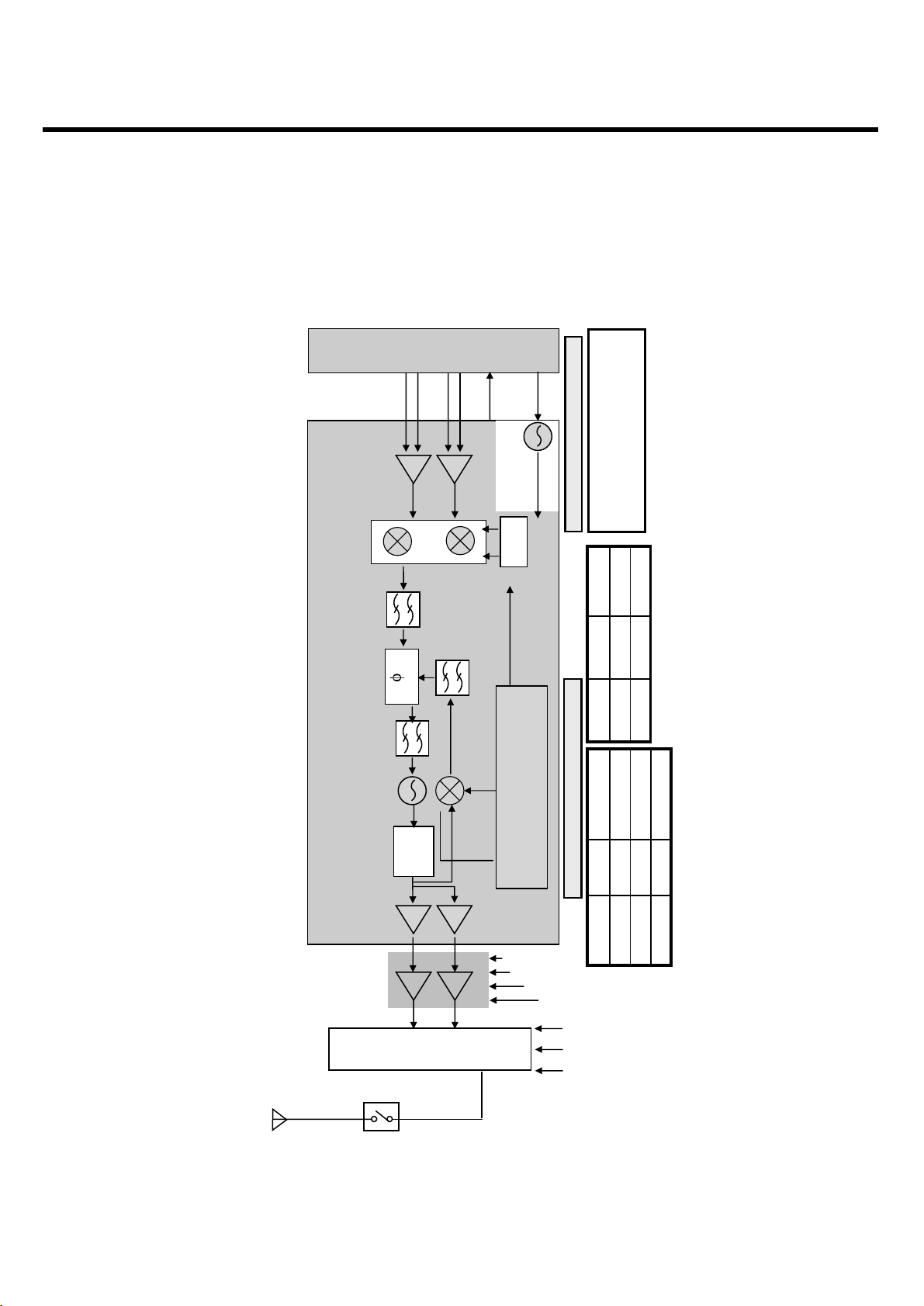
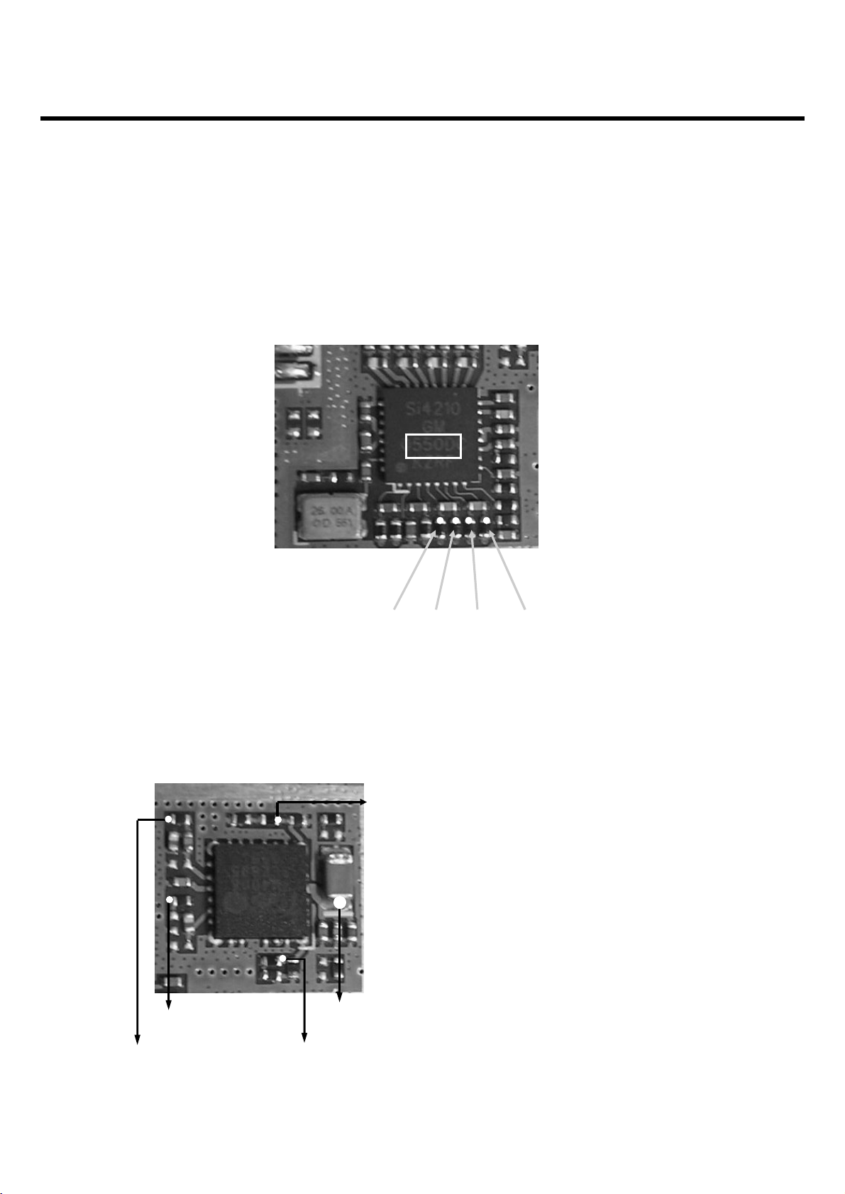
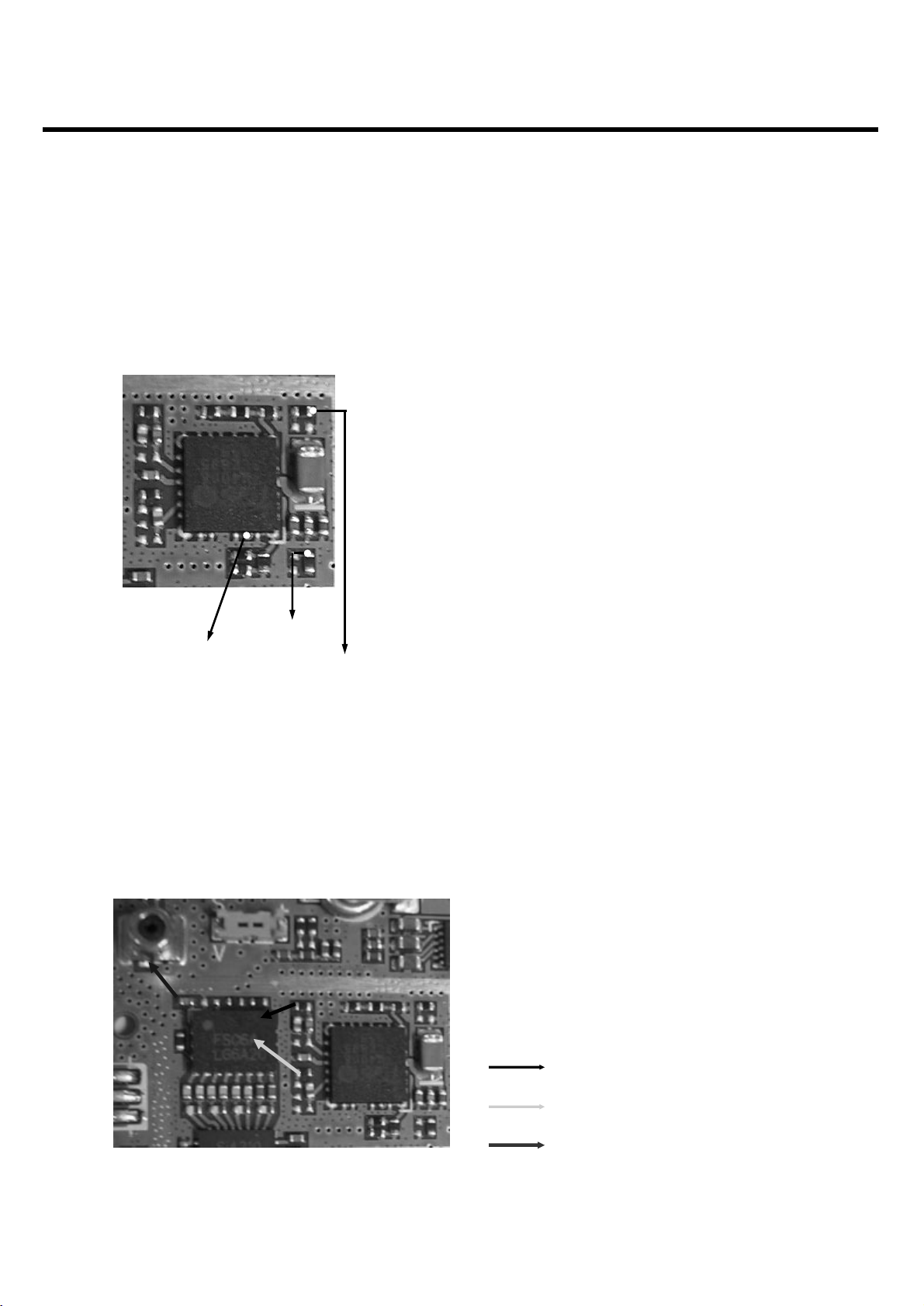
3.2 RF Part Technical Brief
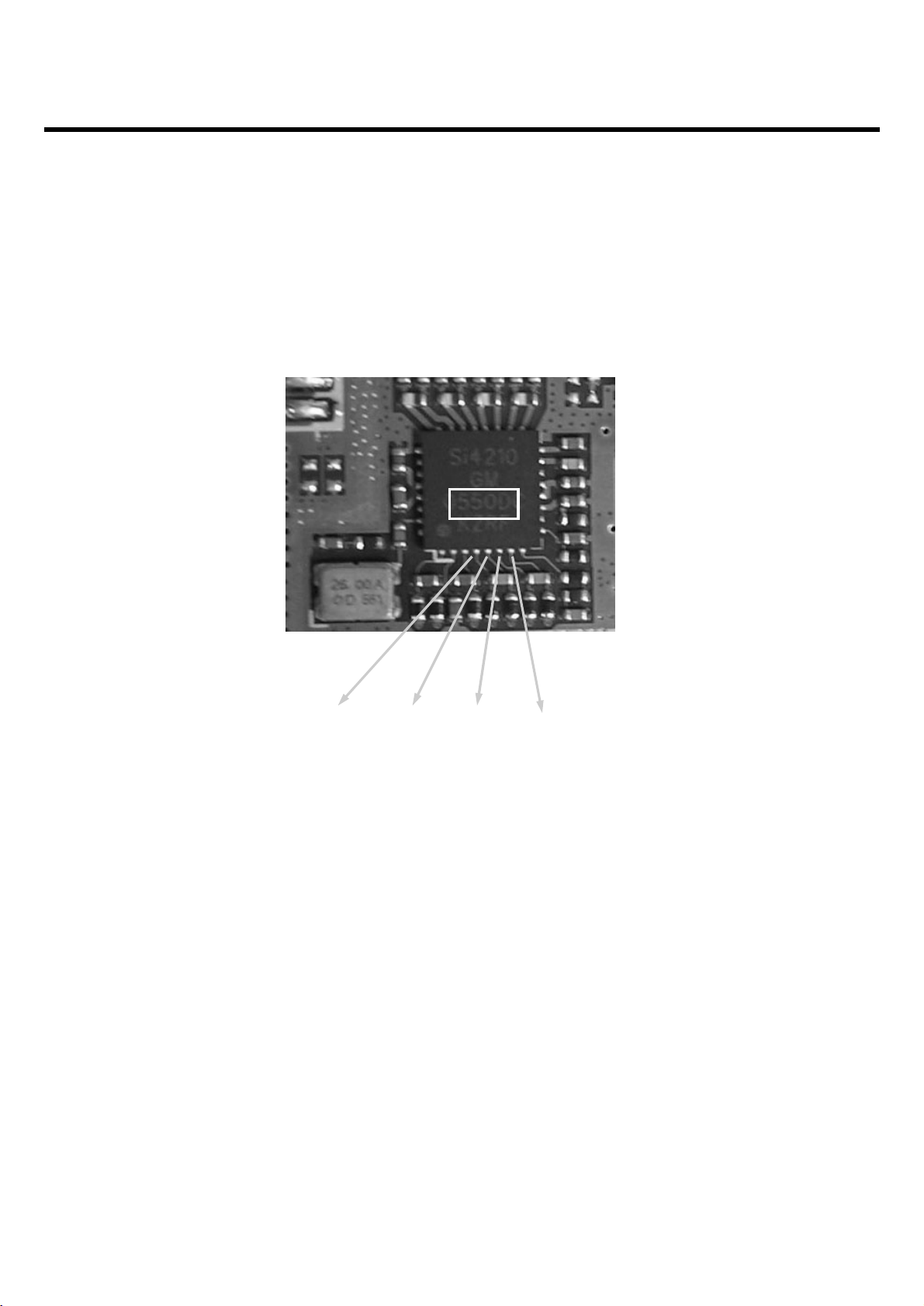
3.2.1 RF Part components
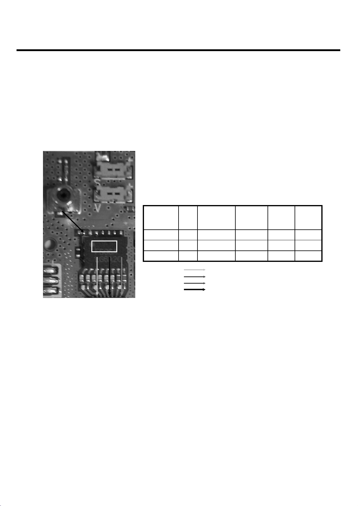
➢
SW501 : Mobile Switch
➢
FL501 : YGHF-S006A
-
FEM
➢
U501 : TQM7M4006
-
Power Amp Module
➢
U502 : SI4210
-
RF Main chip
➢
X501
-
VCTCXO
-
26MHz Clock
SW501
FL501
U501
X501
U502
3. TECHNICAL BRIEF
- 23 -
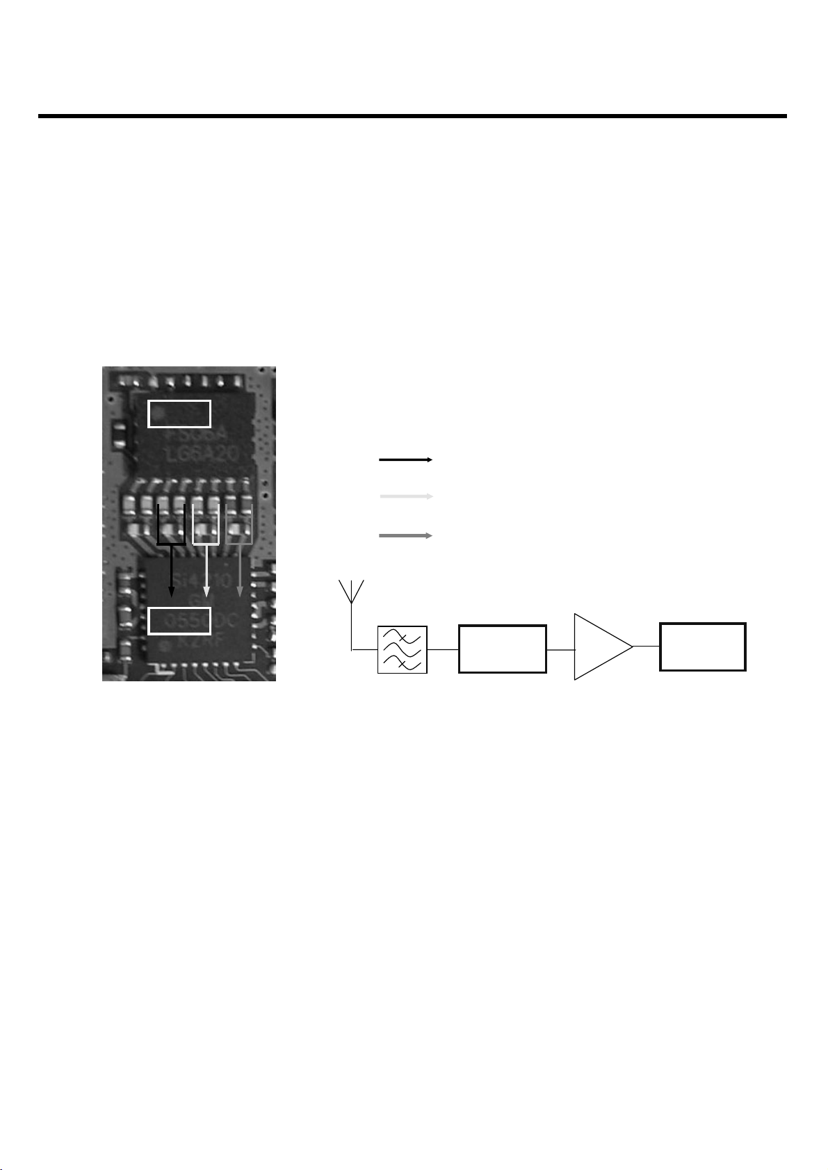
3.2.2 Tx / Rx Part Description(2)
2. Tx/Rx Part component Description
→ VCTCXO
➢
VCTCXO
-
Produce RF reference clock 26MHz frequency
3. Tx/Rx Part component Description
→ RF Main Chip (SI4210)
➢
PDNB, _S_EN, S_CLK, S_DATA
-
From DBB Main Chip Set
-
Contains information all about ARFCN, voice
data, user information etc.
-
RF Chips operate according to these signals
X501
26MHz frequency output
U502
S_CLK
(1pin)
_S_EN
(2pin)
S_DATA
(3pin)
PDNB
(9pin)
3. TECHNICAL BRIEF
- 24 -
3.2.3 Receiver Part Description(1)
1. Rx Block Diagram
BASE BAND
SI-4210
RXIN
RXIP
DAC
ADC
PGA
PGA
RXQN
RXQP
DAC
Channel Filter
ADC
AFC
PDNB
S_EN
S_CLK
S_DATA
26MHz TCXO
TCXO OUT
RX/TX Freq. PLAN
RX GSM900 [925.2 ~ 959.8 MHz]
RX DC1800 [1805.2 ~ 1879.8 MHz]
RX PCS1900 [1930.2 ~ 1989.8 MHz]
Low IF
Rx PCS (1900)
SYNTHESIZER
VCO + FREQUENCY
Rx DCS(1800)
Off
Off
Off
Off
Off
On
GSM900 : 925.2~959.8 MHz
DCS1800 : 1805.2~1879.8 MHz
PCS1900 : 1930.2~1989.8 MHz
MOBILE
SWITCH
/ 2
∏
KMS-507
ANTENNA SWITCH
On
Off
Off
Rx GSM
(900)
RX BAND SELECTION PLAN
MG185c
ANT_SW2
ANT_SW3
ANT_SW1
ANT_SW3
ANT_SW2
ANT_SW1
3. TECHNICAL BRIEF
- 25 -
Receiver Part Description( 2)
2. Rx Part component Description
→ Mobile Switch & FEM
➢
FEM (including Ant. SW & SAW filter)
-
Select the Path - GSM / DCS Tx, GSM / DCS
Rx
-
From DBB, three control signals
(ANT_SW1, ANTSW2, ANTSW3)
FL501
MG185d
Tx
(900
Tx
)
(1800/1900)
Rx GSM
(900)
OnOnANT_SW1
OnOffANT_SW2
OnOffANT_SW3
GSM 900 :Rx Path
DCS : Rx Path
PCS : Rx Path
GSM / PCS Rx Path
Off
On
Off
Rx DCS
(1800)
Off
Off
On
Rx PCS
(1900)
Off
Off
Off

3. TECHNICAL BRIEF
- 26 -
Receiver Part Description(3)
3. Rx Part component Description
→ FEM (BSF Output)
➢
Band Selection Filter
-
Cuts the out of band frequency
FL501
BSF
U502
RF
For GSM : 925MHz 960MHz
For DCS : 1805MHz 1880MHz
For PCS : 1930MHz 1990MHz
LNA
Insertion Loss
For GSM : ~-2.5dB
For DCS : ~-3dB
f
3. TECHNICAL BRIEF
- 27 -
Receiver Part Description(4)
2. Rx Part component Description
→ RF Transceiver Chip (LNA Input)
➢
LNA input port of RF Main Chip(SI4210)
-
Balanced-type LNA Input
FL501
GSM900 LNA Input
U502
DCS LNA Input
PCS LNA Input
BSF
Matching
RF
Circuit
LNA
SI4210
3. TECHNICAL BRIEF
- 28 -
Receiver Part Description(5)
2. Rx Part component Description
→ Rx I/Q signal (SI4210)
U502
RXQN RXQP RXIN RXIP
3. TECHNICAL BRIEF
- 29 -
3.2.4 Transmitter Part Description(1)
1. Tx Block Diagram
BASE BAND
SI-4210
TXIN
Divider
TXIP
DET
2, 4
÷
TXQN
TXQP
AFC
XOUT
26MHz TCXO
TX Freq. PLAN
TCXO OUT
TX GSM900 [880.2 ~ 914.8 MHz]
TX DCS [1710.2 ~ 1784.8 MHz]
TX PCS [1850.2 ~ 1909.8 MHz]
/ 2
÷
OnOnPA_ON
OnOffPA_BAND
High_BandLow Band
OnOffANT_SW2
OnOffANT_SW3
OnOnANT_SW1
SYNTHESIZER
VCO + FREQUENCY
Tx (1800/1900)Tx (900)MG185c
TX BAND SELECTION PLAN
PAM
Triquint
AMP
TQM7M4006
EGSM
MOBILE
SWITCH
KMS-507
VBAT
APC
PA_ON
PA_BAND
DCS/PCS
ANTENNA SWITCH
ANT_SW3
ANT_SW2
ANT_SW1
Transmitter Part Description(2)
2. Tx Part component Description
→ Tx I/Q signal from ABB signal
Transmitter Part Description(3)
2. Tx Part component Description
→ PAM - input and output signals
- 30 -
3. TECHNICAL BRIEF
U502
TXQP TXQN TXIN TXIP
PAM
U501
GSM
OUT
PCS
IN
PCS
OUT
VBAT
GSM
IN
➢
Power Amp Module
-
Amplifies Tx Signal from SI4210
➢
Tx Carrier Frequency
-
GSM : 880 ~ 915MHz
-
DCS : 1710 ~ 1785MHz
-
PCS : 1850 ~ 1910MHz
3. TECHNICAL BRIEF
- 31 -
Transmitter Part Description(4)
2. Tx Part component Description
→ PAM - control signals
Transmitter Part Description(5)
2. Tx Part component Description
→ Mobile Switch & FEM
➢
PA_ON
- From DBB Chip Set
-
Enables Tx Path
➢
PA_Band
-
From DBB Chip Set
-
Select PAM operating band
-
Low : GSM selected
-
High : DCS selected
➢
APC
-
From ABB Chip Set
-
Controls Tx rising and falling shape
- APC voltage Controls Tx Output Power
GSM Tx Path (FEM 6 pin)
DCS/PCS Tx Path (FEM 8 pin)
Tx Path
➢
FEM
-
Select the Path - GSM / DCS Tx, GSM / DCS Rx
-
From DBB, three control signals (ANT_SW1,
ANTSW2, ANTSW3) are fed into the DBB
PAM
U501
PA
BAND(3pin)
PA
ON
APC
 Loading...