

LG MG180C Service Manual
Date: March, 2006 / Issue 1.0
Service Manual
Model : MG180c
Service Manual
MG180c
DIGITAL COMMUNICATION
ABC
GHI
PQRS
JKL
TUV
WXYZ
MNO
DEF

The information in this manual is subject to change without notice and should not be construed as a
commitment by LGE Inc. Furthermore, LGE Inc. reserves the right, without notice, to make changes to
equipment design as advances in engineering and manufacturing methods warrant.
This manual provides the information necessary to install, program, operate and maintain the MG180c.
REVISED HISTORY
DATE ISSUE CONTENTS OF CHANGES S/W VERSION

- 2 -

- 3 -
1. Introduction ..................................... 5
1.1 Purpose................................................... 5
1.2 Regulatory Information............................ 5
1.3 Abbreviations .......................................... 7
2. General Performance...................... 9
2.1 Product Name ......................................... 9
2.2 Supporting Standard ............................... 9
2.3 Main Parts: GSM Solution........................9
2.4 H/W Features.........................................10
2.5 S/W Features .........................................12
3. H/W Circuit Description................ 14
3.1 RF Transceiver General Description..... 14
3.2 Receiver Part ........................................ 14
3.3 Transmitter Part .................................... 17
3.4 Digital Baseband (DBB) Processor........20
3.5 Analog Baseband (ABB) Processor...... 25
4. TROUBLE SHOOTING .................. 43
4.1 Main Components Placement............... 43
4.2 FPCB Components Placement ............. 44
4.3 Baseband Components ........................ 44
4.4 Main Components (Description) ........... 45
4.5 Power On Trouble................................. 46
4.6 Charging Trouble .................................. 47
4.7 LCD Display Trouble............................. 49
4.8 Receiver Trouble................................... 51
4.9 Microphone Trouble .............................. 55
4.10 Vibrator Trouble .................................. 58
4.11 Keypad Backlight Trouble ................... 60
4.12 SIM Detect Trouble ............................. 62
4.13 Earphone Trouble ............................... 64
4.14 RF Rx pass Trouble Shooting............. 68
4.15 RF Tx pass Trouble Shooting ............. 75
5. DOWNLOAD .................................. 83
5.1 Download Setup.................................... 83
5.2 Download Procedure ............................ 84
6. SERVICE AND CALIBRATION ...... 91
6.1 Service S/W ...........................................91
7. CIRCUIT DIAGRAM ....................... 93
8. PCB LAYOUT................................. 98
9. ENGINEERING MODE
....................
101
10. STANDALONE TEST
....................
102
10.1 Setting Method
...............................
102
11. EXPLODED VIEW &
REPLACEMENT PART LIST ..... 103
11.1 EXPLODED VIEW ............................ 103
11.2 Replacement Parts
<Mechanic component>.................... 105
<Main component> ........................... 107
11.3 Accessory ......................................... 117
Table of Contents


1. Introduction
- 5 -
1.1 Purpose
This manual provides the information necessary to repair, calibration, description and download the
features of the MG180c
1.2 Regulatory Information
A. Security
Toll fraud, the unauthorized use of telecommunications system by an unauthorized part (for example,
persons other than your company’s employees, agents, subcontractors, or person working on your
company’s behalf) can result in substantial additional charges you’re your telecommunications
services. System users are responsible for the security of own system. There are may be risks of toll
fraud associated with your telecommunications system. System users are responsible for
programming and configuring the equipment to prevent unauthorized use. LGE does not warrant that
this product is immune from the above case but will prevent unauthorized use of common-carrier
telecommunication service of facilities accessed through or connected to it. LGE will not be
responsible for any charges that result from such unauthorized use.
B. Incidence of Harm
If a telephone company determines that the equipment provided to customer is faulty and possibly
causing harm or interruption in service to the telephone network, it should disconnect telephone
service until repair can be done. A telephone company may temporarily disconnect service as long as
repair is not done.
C. Changes in Service
A local telephone company may make changes in its communications facilities or procedure. If these
changes could reasonably be expected to affect the use of the MG180c or compatibility with the
network, the telephone company is required to give advanced written notice to the user, allowing the
user to take appropriate steps to maintain telephone service.
D. Maintenance Limitations
Maintenance limitations on the MG180c must be performed only by the LGE or its authorized agent.
The user may not make any changes and/or repairs expect as specifically noted in this manual.
Therefore, note that unauthorized alternations or repair may affect the regulatory status of the system
and may void any remaining warranty.
1. Introduction

1. Introduction
- 6 -
E. Notice of Radiated Emissions
The MG180c complies with rules regarding radiation and radio frequency emission as defined by local
regulatory agencies. In accordance with these agencies, you may be required to provide information
such as the following to the end user.
F. Pictures
The pictures in this manual are for illustrative purposes only; your actual hardware may look slightly
different.
G. Interference and Attenuation
An MG180c may interfere with sensitive laboratory equipment, medical equipment, etc. Interference
from unsuppressed engines or electric motors may cause problems.
H. Electrostatic Sensitive Devices
ATTENTION
Boards, which contain Electrostatic Sensitive Device (ESD), are indicated by the sign. Following
information is ESD handling:
• Service personnel should ground themselves by using a wrist strap when exchange system boards.
• When repairs are made to a system board, they should spread the floor with anti-static mat which is
also grounded.
• Use a suitable, grounded soldering iron.
• Keep sensitive parts in these protective packages until these are used.
• When returning system boards or parts like EEPROM to the factory, use the protective package as
described.

1. Introduction
- 7 -
1.3 Abbreviations
For the purposes of this manual, following abbreviations apply:
APC Automatic Power Control
BB Base Band
BER Bit Error Ratio
CC-CV Constant Current - Constant Voltage
DAC Digital to Analog Converter
DCS Digital Communication System
dBm dB relative to 1 milli watt
DSP Digital Signal Processing
EEPROM Electrical Erasable Programmable Read-Only Memory
EL Electroluminescence
ESD Electrostatic Discharge
FPCB Flexible Printed Circuit Board
GMSK Gaussian Minimum Shift Keying
GPIB General Purpose Interface Bus
GSM Global System for Mobile Communications
IPUI International Portable User Identity
IF Intermediate Frequency
LCD Liquid Crystal Display
LDO Low Drop Output
LED Light Emitting Diode
OPLL Offset Phase Locked Loop
PAM Power Amplifier Module

1. Introduction
- 8 -
PCB Printed Circuit Board
PGA Programmable Gain Amplifier
PLL Phase Locked Loop
PSTN Public Switched Telephone Network
RF Radio Frequency
RLR Receiving Loudness Rating
RMS Root Mean Square
RTC Real Time Clock
FEM Front End Module
SIM Subscriber Identity Module
SLR Sending Loudness Rating
SRAM Static Random Access Memory
STMR Side Tone Masking Rating
TA Travel Adapter
TDD Time Division Duplex
TDMA Time Division Multiple Access
UART Universal Asynchronous Receiver/Transmitter
VCO Voltage Controlled Oscillator
VCTCXO Voltage Control Temperature Compensated Crystal Oscillator
WAP Wireless Application Protocol
2. General Performance
- 9 -
2.1 Product Name
MG180c : Support GPRS (Class 10)
2.2 Supporting Standard
2.3 Main Parts: GSM Solution
2. General Performance
Item Feature Comment
E-GSM/DCS/PCS Triple Band
Supporting Standard Phase 2+
SIM Toolkit : Class 1,2,3
EGSM TX : 880 - 915 MHz
EGSM RX : 925 -960 MHz
DCS TX : 1710 - 1785 MHz
Frequency Range
DCS RX : 1805 - 1880 MHz
PCS TX : 1850 - 1910 MHz
PCS RX : 1930 - 1990 MHz
WAP 1.2.1
Application Standard
MMS
MG180c
Digital Baseband Calypso-AMR C035(D751992GHH)
Analog Baseband IOTA(TWL3025)
RF Chip Aero-2 (SI4210)

2. General Performance
- 10 -
2.4 H/W Features
Item Feature Comment
Form Factor Single Color BAR Main LCD : CSTN, 101 x 80
1) Capacity
Battery
Standard : Li-Ion 830mAh
Packing Type: Inner Pack
Size Standard : 101 x 44 x 15.9 mm L x W x H
Weight 72.5 g With Battery
PCB Main PCB : 8Layers, 1t
AVG TCVR Max : 120mA (Power Level 19)
current (mA) Max : 310mA (Power Level 5)
Standby Current 4 mA @ Paging Period 6
Standby time Up to 200 hours @ Paging Period 6
Charging time Below 3 hours @ Power Off /1000mAh
Talk time Min 2.5hr @Power Level 5 @ 800 mAh
RX sensitivity
EGSM : -105 dBm
DCS : -105 dBm, PCS : -105 dBm
TX output power
EGSM : 32.5 dBm Class4 (GSM850, EGSM )
DCS : 30.5 dBm, PCS : 30 dBm Class1 (DCS, PCS)
GPRS compatibility GPRS Class 10
SIM card type Plug-In SIM 3V
-Main LCD : 65K CSTN (101 x 80)
Display
-Backlight : White
Alphanumeric Key : 12 Function Key:
Keypad Function Key : 9 4 Key Navigation,
Total Number of Keys : 21 F1, F2, SND, END/PWR, Clear
2. General Performance
- 11 -
Item Feature Comment
Antenna Internal Type
Triple-band
System connector 24 Pin
Ear Phone Jack 3 Pole (φ2.5mm)
PC synchronization No CDROM
Memory Flash : 64Mbit / SRAM :32Mbit Spansion
Speech coding FR, EFR, HR, AMR
Data & Fax Built in Data & Fax support
Vibrator Built in Vibrator
MIDI
40 Poly
Buzzer Function By Using
(for Buzzer Function) MIDI IC
Voice Recording No
Travel Adapter Yes
Ear-Microphone
Options Data Cable
Cigarette Lighter Adapter

2.5 S/W Features
2. General Performance
- 12 -
Item Feature Comment
RSSI 0~5 level
Battery Charging 0~4 level
Key Volume 0~5 level
Keypad Volume 0~5 level
Effect sound volume 0~5 level
Ring Volume 0~5 level
Time/Date Display Yes
Text Input T9
Multi-language Yes
Quick Access Mode
Phone Book / Web Access / Sound
/ Message / IM / Gallery
PC Sync Schedule/Phonebook/SMS MS Scheduler & Outlook
Speed Dial Yes (2~9) Voice mail center → 1 key
Profile Yes
CLIP/CLIR Yes
Phonebook 3 Number + 1 Memo + 1 e-mail Phone (Up to 255 entries)
Last Dial Number Yes (20)
Last Received Number Yes (20)
Last Missed Number Yes (10)
Search Number/Name Yes
Group 7 / User Editor
Fixed Dial Number Yes
Voice Memo 30 secs * 3
Call Remainder Yes
Network Selection Automatic / Manual
2. General Performance
- 13 -
Item Feature Comment
Mute Yes
Call Divert Yes
Call Barring Yes
Call Charge Yes
Call Duration Yes
SMS (EMS) 100
Melody/Picture/Animation
Send/Receive/Save
MMS Yes
WAP Browser WAP 2.0
Java CLDC v1.0.3 / MIDP v1.0.3
Wall Paper Yes Max. 10 preset
Download Melody/
Over the WAP
Wallpaper (MMS)
Long Message Max. 918 Character(6page*153)
Cell Broadcast Yes
Calendar Yes
Memo 20
World Clock Yes
Unit Convert Length/Surface/Volume/Weight
Fax & Data Yes
SIM Lock Yes Operator Dependent
SIM Toolkit Class 1,2,3
Phone lock Yes
Security DRM (Forward-lock only)
CPHS Yes
IM Yes
3. H/W Circuit Description
- 14 -
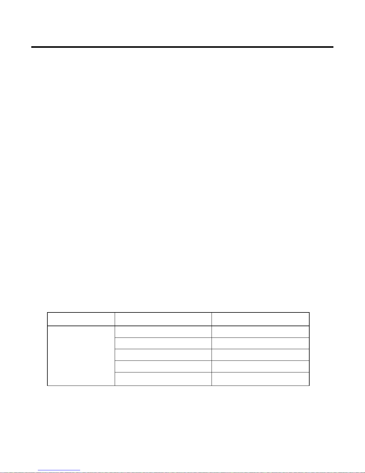
3.1 RF Transceiver General Description
The RF parts consist of a transceiver part, a power amplifier part, a front-end module part, a voltage
supply part, and a VC-TCXO part.
The AeroII transceiver is composed of single RF chipset, Si4210-GM[U501] which is a quad-band
GSM/GPRS wireless communications. This device integrated a receiver based on a low IF (200KHz)
architecture and a transmitter based on modulation loop architecture. The transceiver employed a 3
wire serial interface to allow an external system controller to write the control registers for dividers,
receive path gain, power down setting, and other controls.
3.2 Receiver Part
The receiver part uses a low-IF receiver architecture that allows for the on-chip integration of the
channel selection filters, eliminating the external RF image reject filters and the IF SAW filter required
in conventional super-heterodyne architecture.
The Si4210-GM[U501] integrates four differential input LNAs that are matched to the 200 Ohm
balanced-output SAW filters through external LC matching networks. A quadrature image-rejection
mixer downconverts the RF signal to a 200kHz intermediate frequency (IF) with the RFLO from the
frequency synthesizer.
The mixer output is amplified with an analog programmable gain amplifier (PGA) and quadrature IF
signal is digitized with high resolution A/D converters (ADCs). The Si4210-GM[U501] downconverts
the ADC output to baseband with a digital 200kHz quadrature LO signal. Digital decimation and IIR
filters perform digital filtering , and remove blocking and reference interference signals. After filtering,
the digital output is scaled with digital PGA, which is controlled with the DGAIN[5:0] bits in register 20h.
The amplified digital output signal go through with DACs that drive a differential analog signal onto the
RXIP,RXIN,RXQP and RXQN pins to interface to standard analog ADC input baseband ICs.
3. H/W Circuit Description
Table 3-1. Antenna Display
Antenna Bar Number Rx Power (dBm)
5 → 4 -85dBm±2dBm
4 → 3 -90dBm±2dBm
Antenna Display 3 → 2 -95dBm±2dBm
2 → 1 -100dBm±2dBm
1 → 0 -105dBm±2dBm

3. H/W Circuit Description
- 15 -
3.2.1. RF Front End
RF front end consists of Front End Module(FL500), quad band LNAs integrated in transceiver(U502).
The Received RF signals (GSM-850 869MHz ~ 894MHz, EGSM 880 MHz ~ 960MHz, DCS 1710 MHz
~ 1880 MHz, PCS 1930MHz ~ 1990MHz) are fed into the antenna or mobile switch.
An antenna matching circuit is between the antenna and the mobile switch. The Front End
Module(FL500) is used for control the Rx and TX paths. And the input signals ANT_SW1 and
ANT_SW2 of a FL500 are directly connected to baseband controller to switch either TX or RX path on.
Front End Module(FL500) is an antenna switch module for Quad band phone. The logic and current is
given below Table 3-2.
ADC
ADC
ADC
ADC
Digital Filter
Digital Filter
DAC
DAC
DAC
DAC
LOW
IF
LOW
IF
D
I
P
D
I
P
GSM
850
DCS
FL500
Front End Module
26MHz
I
Q
U502/Si4210
VCO + FREQUENCY
SYNTHESIZER
VCO + FREQUENCY
SYNTHESIZER
0/
90
0/
90
PGA PGA
X501
VC-TCXO
GSM
850
DCS
PCS
LNA
Baseband
(TI)
U100
(Calypso +)
+
U100
(IOTA)
Baseband
(TI)
U100
(Calypso +)
+
U100
(IOTA)
PCS
EGSM
EGSM
Figure 1. RF Receiver Block
Table 3-2. The Logic and Current
ANT_SW1(PIN 15) ANT_SW1 2(PIN 14) Current
GSM 850/EGSM RX 0 V 0 V < 0.1 mA
DCS/PCS RX 2.5~3.0 V 0 V < 0.1 mA
GSM-850/EGSM TX 0 V 2.5~3.0 V < 0.1 mA
DCS/PCS TX 2.5~3.0 V 2.5~3.0 V < 0.1 mA

3. H/W Circuit Description
- 16 -
3.2.2. Synthesizer
The Aero II transceiver integrates two complete PLLs including VCOs, varactors, resonators, loop
filters, reference and VCO dividers, and phase detectors. The RF PLL uses two multiplexed VCOs.
The RF1 VCO is used for receive mode, and the RF2 VCO is used for transmit mode. The IF PLL is
used only during transmit mode. All VCO tuning inductors are also integrated. The IF and RF output
frequencies are set by programming the N-Divider registers, NRF1, NRF2 and NIF. Programming the
N-Divider register for either RF1 or RF2 automatically selects the proper VCO.
Transmit modes should always use f∅ = 200kHz. The IF and RF output frequencies are set by
programmi ng the N-Divider registers and also programmed via 3-wire interface with external system
controler.
Serial
I/O
Serial
I/O
Baseband
(TI)
U100
IOTA
+
U100
Calypso-
Baseband
(TI)
U100
IOTA
+
U100
Calypso-
U502/Si4210
RF1
RF2
PDIB
26MHz
X501
VC-TCXO
SCLK
SDIO
SEN
PDN
XTAL1
XOUT
XEN
Power
control
Power
control
Self
Tune
Self
Tune
1/N
1/N
1/N
1/N
DET
DET
Self
Tune
Self
Tune
DET
DET
To Rx/Tx
To Tx
RF PLL
IF PLL
PDRB
SDOSEL[4:0]
N
IF
[15:0]
N
RF1
[15:0]
N
RF2
[15:0]
1,2
1,2
65,130
65,130
Figure 2. Synthesizer Block
3. H/W Circuit Description
- 17 -
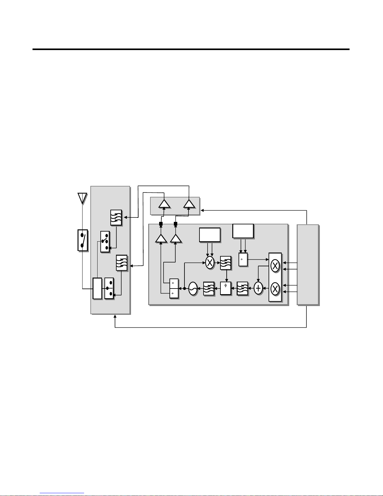
3.3 Transmitter Part
The Transmitter part contains the transmitter parts of Si4210-GM[U501], Power Amp Module[U501]
and Front End Module[FL500]. The transmit section of Si4210-GM[U502] consists of an I/Q base band
up_converter, an offset phase-locked loop(OPLL) and two output buffers that can drive external power
amplifiers(PA). The RF GMSK outputs from the transmit VCO are fed directly to the RF power
amplifiers. The peak output power and the profile of the transmitted burst are controlled by means of
incorporated pow er control circuits inside of PA and DAC output from the Base band Controller. The
PA outputs pass to the antenna connector via Front End Module.
DET
DET
2
2
1
1
2
2
IF PLL
IF PLL
I
Q
Baseband
(TI)
U100
IOTA
+
U100
Calypso-
Baseband
(TI)
U100
IOTA
+
U100
Calypso-
PA_BAND
ANT_SW1,ANT_SW2
RFOG
RFOD
GSM 850/
EGSM
DCS/ PCS
RF PLL
RF PLL
D
I
P
D
I
P
DCS
FL500
Front End Module
PCS
GSM 850/
EGSM
Si4210 (U502)
PAM RF3166 (U501)
PA PA
Figure 3. RF Transmit Block
3. H/W Circuit Description
- 18 -
3.3.1. Power Amplifier
The RF3166 [U500] is a quad-band EGSM 900/GSM 850/DCS/PCS power amplifier module that
incorporat es an indirect closed loop method of power control. The indirect closed loop is fully selfcontained and it do es not require loop optimization. It can be driven directly from the DAC output in
the baseband circuit. On-board power control provides over 37 dB of control range with an analog
voltage input(Vramp). Efficien cy is 60% at GSM and 55% at DCS/PCS.
3.3.2. 26MHz Clock
The 26 MHz clock consists of a TCXO(Temperature Compensated Crystal Oscillator) which oscillates
at a frequency of 26 MHz. It is used within the Si4210 RF Main Chip, BB Analog chip-set(IOTA), Digita
l chip-set(Calypso-).
Figure 5. VC-TCXO Circuit
26MHzX500
2
GND
3
OUT
VCC
4
VCONT
1
C531
1uF
1000p
C530
RF2.85V
1000p
C532
R515
12K
TCXO_OUTAFC
3. H/W Circuit Description
- 19 -
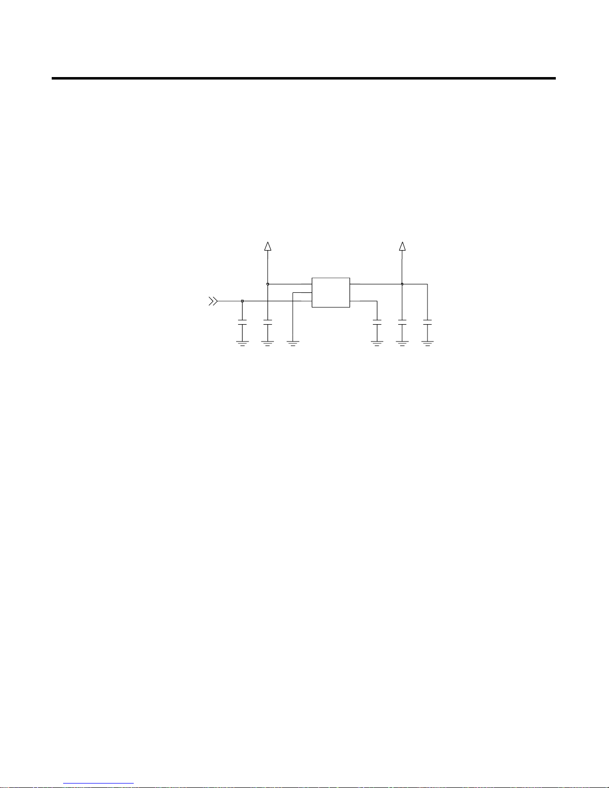
3.3.3. Power Supplies and Control Signals
An external regulator(U502) is used to provide DC power to RF part. Every RF component except
power amp module uses this external regulator.
Figure 6 External regulator Circuit
C536
NA 4.7u
C535
1u
C537
C534
4.7u
R1114N281D-TR-F
U502
CE
3
2
GND
NC
4
1
VDD5VOUT
C533
1000p
VBAT
RF2.85V
RF_EN

3. H/W Circuit Description
- 20 -
3.4 Digital Baseband (DBB) Processor
3.4.1. General Description
CALYPSO is a chip implementing the digital base-band processes of a GSM/GPRS mobile phone.
This chip combines a DSP sub-chip (LEAD2 CPU) with its program and data memories, a Micro- Controller core with emulation facilities (ARM7TDMIE), internal 8Kb of Boot ROM memory, 4M bit
SRAM memory, a clock squarer cell, several compiled single-port or 2-ports RAM and CMOS gates.
The chip will fully support the Full-Rate, Enhanced Full-Rate and Half-Rate speech coding. CALYPSO
implements all features for the structural test of the logic (full-SCAN, BIST, PMT, JTAG
boundary-SCAN).
Figure 7. Top level block diagram of the Calypso-

3. H/W Circuit Description
- 21 -
3.4.2. Block Description
CALYPSO architecture is based on two processor cores ARM7 and DSP using the generic RHEA bus
sta ndard as interface with their associated application peripherals.
CALYPSO is composed from the following blocks:
• ARM7TDMIE : ARM7TDMI CPU core
• DSP sub chip
• ARM peripherals
General purpose peripherals
• ARM Memory Interface for external RAM, Flash or ROM
• 4 Mbit Static RAM with write-buffer
Application peripherals
• ARM General purposes I/O with keyboard interface and two PWM modulation signals
• UART 16C750 interface (UART_IRDA) with
→IRDA control capabilities (SIR)
→Software flow control (UART mode).
• UART 16C750 interface (UART_MODEM) with
→Hard ware flow protocol (DCD, CTS/RTS)
→Auto baud function
• SIM Interface.
• TPU(Time Processing Unit) : Processing for GSM time base
• TSP(Time Serial Port) : GSM data interface with RF and ABB
Memory Interface : External/Internal Memory Interface
nCS0 : FLASH1, 16bit access, 3 wait state
nCS1 : FLAHS2, 16bit access, 3 wait state
nCS2 : Ext SRAM, 16bit access, 3 wait state
nCS3 : Main LCD(16bit access), OEL(8bit access) addressing, 3 wait state
nCS4 : MIDI(8bit access), USB(8bit access) addressing, 3 wait state
nCS6 : Int SRAM, 32bit access, 0 wait state
• Calypso is internaly 39MHz machine (25ns machine cycle), so it requires 3 wait-state for 80ns
access(25*4 = 100 ns).
3. H/W Circuit Description
- 22 -
3.4.3. RF Interface (TPU, TSP Block)
Calypso uses this interface to control IOTA_CS(ABB Processor) and AERO(RF Processor) with GSM
Time Base
TSP (Time Serial Port)
Resource Interconnection Description
TSPDO ABB & RF main Chip Control Data
TSPDI/IO(4) GPIO4
TSPEN0 ABB ABB Control Data Enable Signal
TSPEN1 STROBE STROBE Control Data Enable Signal
TSPCLKX CLK CLK Control Data Enable Signal
TPU (Parallel Port)
TSPACT0 PDNB RF main Chip Reset Signal
TSPACT01 PA_ON Power Amp ON signal
TSPACT02 PA_BAND Power Amp band-selection signal
TSPACT03 ANT_SW1 FEM control signal
TSPACT04 ANT_SW2 FEM control signal
Table 3-4. RF Interface Spec.
3. H/W Circuit Description
- 23 -
3.4.4. SIM Interface
SIM interface scheme is shown in (Figure 8).
SIM_IO, SIM_CLK, SIM_RST ports are used to communicate DBB with ABB and the Charge Pump in
ABB enables 1.8V/3V SIM operation.
SIM Interface
SIM_CLK SIM card reference clock
SIM_RST SIM card async/sync reset
SIM_IO SIM card bidirectional data line
SIM_PWCTRL SIM card power activation
SIM_CD SIM card presence detection
3.4.5. UART Interface
MG180c has two UART Drivers as follow :
UART : Hardware Flow Control / Fax & Data Modem
SIM_IO
SIM_CLK
SIM_RST
SIM_PWRCTRL
SIM_CD
DBB ABB
VRSIM
DBBSIO
DBBSCK
DBBSRST
SIMCLK
S IMIO
SIMRST
SIM
VPP
CLK
IO
RST
V_IO
22p
100k
V_SIM
0.1u
10k
10k
Figure 8. SIM Interface
3. H/W Circuit Description
- 24 -
UART MODEM (UART1)
Resource Name Description
TX_MODEM TXD Transmit Data
RX_MODEM RXD Receive Data
CTS_MODEM CTS Clear To Send
RTS_MODEM RTS Request To Send
GPIO 3 DSR Data Set Ready
Table 3-5. UART Interface spec.

3. H/W Circuit Description
- 25 -
3.4.6. GPIO Map
In total 16 allowable resources, MG180c is using 13 resources except 3 resources dedicated to SIM
and Memory. MG180c GPIO (General Purpose Input/Output) Map, describing application, I/O state,
and enable level, is shown in below table.
3.5 Analog Baseband (ABB) Processor
3.5.1. General Description
IOTA is Analog Baseband (ABB) Chip supports GSM900,DCS1800, PCS1900, GPRS Class 10 with
Digital Basband Chip (Calypso). IOTA processes GSM modulation/demodulation and power
management operations.
Block Description
• Audio Signal Processing & Interface
• Baseband in-phase(I), quadrature(Q) Signal Processing
• Auxiliary RF converters
• Five-channel analog-to-digital converters (ADC)
I/O # Net Name I/O Resource State Inactive State Active State
I/O (0) IF_MODE O GPIO
LOW HIGH
(8080 mode) (6400 mode)
I/O (1) MELODY_INT I GPIO HIGH LOW
I/O (2) LCD_ID
I
I GPIO
LOW HIGH
(?) (?)
I/O (3) DSR (Note 1) I GPIO HIGH LOW
I/O (4)
LCD_BACKLIGHT
O GPIO LOW HIGH
(Note 2)
I/O (5) SIM_PWCTL O SIM
I/O (6) VOICEMAIL_EN O GPIO LOW HIGH
I/O (7) LCD_RESET O GPIO
HIGH LOW
(Normal Operation) (Reset)
I/O (8) NOT USE O GPIO
I/O (9) PCM_TX / Not used O DAI / GPIO (Note 2) (Note 2)
I/O (10) PCM_RX O DAI /GPIO (Note 2) (Note 2)
I/O (11) PCM_CLK / Not used O DAI / GPIO (Note 2) (Note 2)
I/O (12) PCM_SYNC / Not used O DAI / GPIO (Note 2) (Note 2)
I/O (13) NOT USE O GPIO
I/O (14) NBHE O MEMORY
I/O (15) NBLE O MEMORY
Table 3-6. GPIO Map Table
• Six Low-dropout (LDO), linear voltage regulators targeted core, general I/O, memory I/O, SIM I/O
• High voltage (20V) Li-Ion or Ni-MH battery charging control
• Voltage detectors (with power-off delay)
• Voice Codec
3. H/W Circuit Description
- 26 -
MCU
Serial Port
(USP)
Clock Gene
(CKG)
Internal
Bus
Controller
(IBIC)
Test Access
Port
(TAP)
Voiceband
Serial Port
(VSP)
Auxiliary
Drivers
(ACD)
Voltage
Reference
Power
Control
(VRPC)
Voltage Regulation
(VREG)
APC
AFC
ADAC
Timing
Serial Port
(TSP)
Baseband
Codec
(BBC)
Voiceband
Codec
(VBC)
Monitoring
ADC
(MADC)
Battery Charger
Interface
(BCI)
VBAT
VBACKUP
VCHG
BFSR
BDR
BFSX
BDX
UDX
UDR
UEN
CK13M
TMS
TCK
TDI
TDO
VCK
VFS
VDX
VDR
LEDA
LEDC
LEDB1
LEDB2
GNDL1
GNDL2
ON_nOFF
RESPWONz
CK32K
RPWON
PWON
ITWAKEUP
TESTRSTz
VREF
REFGND
IBIAS
APC
AFC
DAC
TDR
TEN
TEST1/INT1
TEST2/INT2
TEST3
TEST4
BULIP
BULIM
BULQP
BULQM
BDLIP
BDLIM
BDLQP
BDLQM
EARP
EARN
AUXOP
AUXON
AUXI
HSO
HSMICP
HSMICBIAS
MICIP
MICIN
ADIN1
ADIN2
ADIN3
PCHG VCCS VBAT
Double
Bounding
Pads
Baseband
Serial Port
(BSP)
Backup
(BREG)
VBACKUP
VRRTC
UPR
VLRTC
GNDD
VCMEM
VLMEM
VRMEM
VRRAM
VCDBB
VRDBB
VSDBB
VCIO
VRIO
VRSIM
GNDA
VRABB
VCABB
TESTV
MICBIAS
GNDAV
SIM CARD
Interface
(SIM)
DBBSCK
DBBSIO
DBBSRST
ICHG
ADIN4
SIMCK
SIMIO
SIMRST
ICTL VCHG VBATS
VXRTC
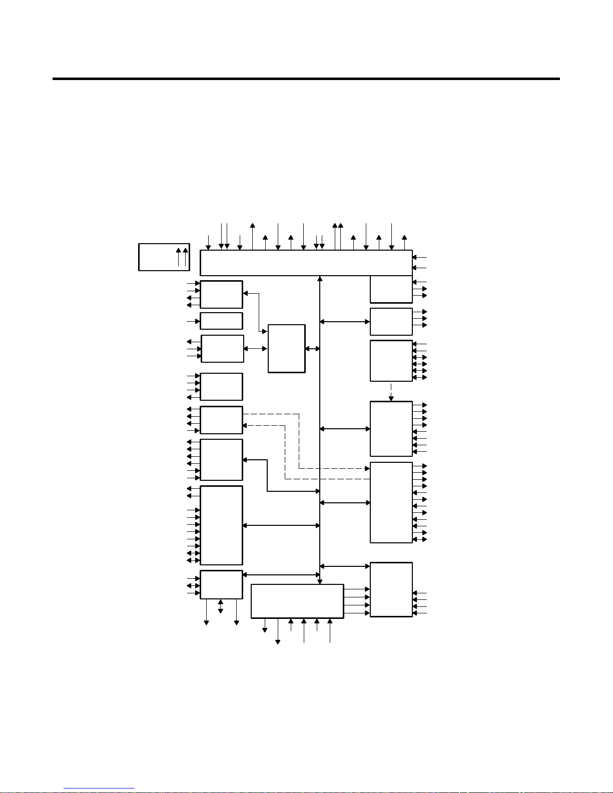
Figure 9. Top level block diagram of the IOTA(TWL3025)
3. H/W Circuit Description
- 27 -
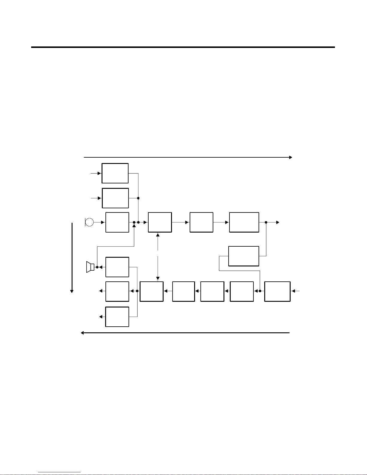
3.5.2. Audio Signal Processing & Interface
The voice codec circuitry processes analog audio components in the voice uplink (VUL) path and
applies this signal to the voice signal interface for eventual baseband modulation. In the voice
downlink (VDL) path, the codec circuitry changes voice component data received from the voice serial
interface (VSP) into analog audio.
Figure 10. Audio Interface Block Diagram
AUXI
4.6 dB or
28.2 dB
MICAMP
25.6 dB
365 mV
RMS
Sensitivity
49.3 dBv/Pa
620 mV
RMS
32.5 mV
RMS
1.385 V
RMS
Sensitivity
106.7 dBspl/Vrm
692 mV
RMS
EARAMP
1 dB
AUXAMP
5 dB
HSOAMP
5 dB
1.237 V
RMS
VREF 1.75 V
1b + 1b
ADC
2.48 dB
UL Filter
3.25 dB
PGA:
Gain: 0 dB
12 dB to 12 dB
1-dB Step
Sidetone:
1 dB to 23 dB
Mute
SLR = (8 dB 3 dB)
RLR = (2 dB 3 dB)
DAC and
Smoothing
Filter 0 dB
4b
Digital
Modulator
0 dB
Volume
Control
0 dB to 24 dB
+ Mute
DL Filter
0 dB
PGA
Gain: 0 dB
6 dB to 6 dB
1-dB Step
3 dBm0
Full Scale
16 Bits
3 dBm0
Full Scale
16 Bits
STMR = (13 dB 5 dB)
346 mV
RMS
HSMICP
18 dB
78 mV
RMS
±
±
±
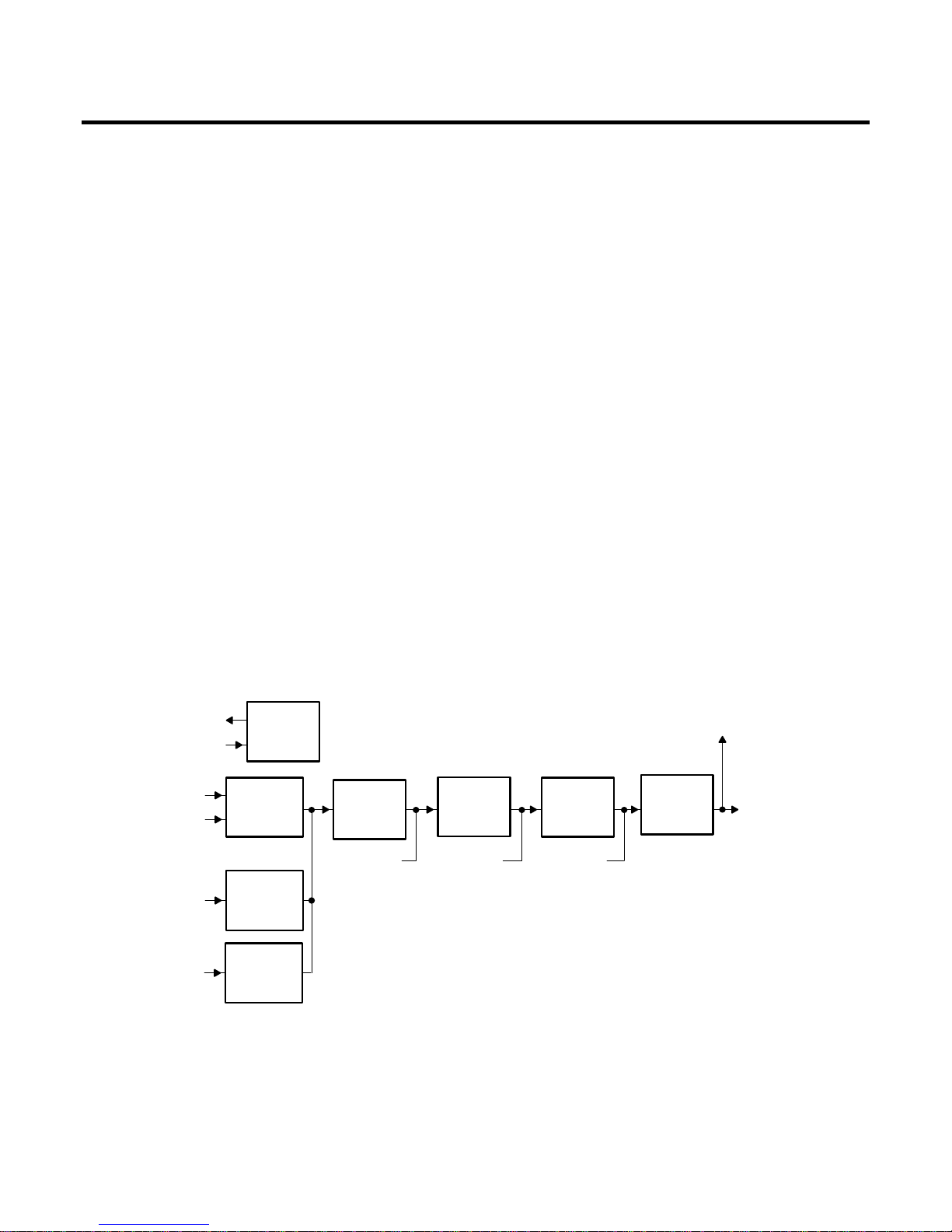
3.5.3. Audio uplink processing
The VUL path includes two input stages. The first stage is a microphone amplifier, compatible with
electret microphones containing a FET buffer with open drain output. The microphone amplifier has
again of typically 25.6 dB ( 1 dB) and provides an external voltage of 2.0 V or 2.5 V to bias the
microphone (MICBIAS). The auxiliary audio input can be used as an alternative source for higher level
speech signals. This stage performs single-ended-to differential conversion and provides a
programmable gain of 4.6 dB or 28.2 dB. The third stage is a headset microphone amplifier,
compatible with electret microphones. The headset microphone amplifier has a gain of typically 18 dB
and provides an external voltage of 2.0 V or 2.5 V to bias the headset microphone (HSMICBIAS).
When one of the input stages (MICI, AUXI, HSMICP) is in use, the two other input stages are disabled
and powered down. The resulting fully differential signal is fed to the analog-to-digital converter (ADC).
The ADC conversion slope depends on the value of the internal voltage reference. Analog-to-digital
conversion is performed by a third-order !-" modulator with a sampling rate of 1 MHz. Output of the
ADC is fed to a speech digital filter, which performs the decimation down to 8 kHz and band-limits the
signal with both low-pass and high-pass transfer functions. Programmable gain can be set digitally
from -12 dB to +12 dB in 1-dB steps and is programmed with bits 4-0 (VULPG(4:0)) of the voiceband
uplink register. The speech samples are then transmitted to the DSP via the VSP at a rate of 8 kHz.
There are 15 meaningful output bits. Programmable functions of the VUL path, power-up, input
selection, and gain are controlled by the BSP or the USP via the serial interfaces. The VUL path can
be powered down by bit 0 (VULON) of the power down register.
3. H/W Circuit Description
- 28 -
SINC
Filter
Microphone
Amplifier
25.6 dB
UpLinkIIR
Bandpass
Filter 3.52 dB
Bias
Generator
To Voice
Serial
Interface
fs1 = 1 MHz
fs2 = 40 kHz
fs3 = 8 kHz
MICIP
MICIN
AUXI
MICBIAS
PGA
12 dB to
Auxiliary
Amplifier
4.6 dB
Side Tone to Voice Downlink
28.2 dB
12 dB
Modulator
2.48 dB
HSMICP
Auxiliary
Amplifier
18 dB
HSMICBIAS
∑-∆
Figure 11. Uplink Path
3. H/W Circuit Description
- 29 -
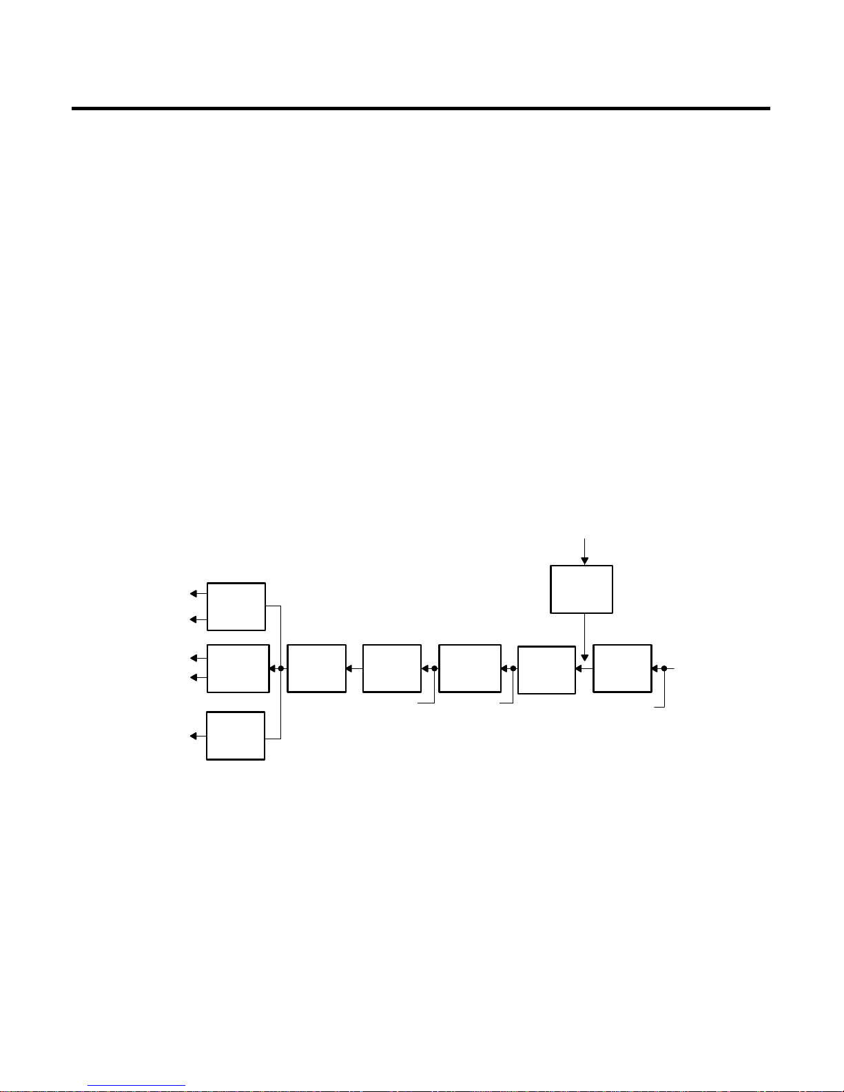
3.5.4. Audio downlink processing
The VDL path receives speech samples at the rate of 8 kHz from the DSP via the VSP and converts
them to analog signals to drive the external speech transducer. The digital speech coming from the
DSP is first fed to a speech digital filter that has two functions. The first function is to interpolate the
input signal and to increase the sampling rate from 8 kHz up to 40 kHz to allow the digital-to-analog
conversion to be performed by an oversampling digital modulator. The second function is to band-limit
the speech signal with both low-pass and high-pass transfer functions. The filter, the PGA gain, and
the volume gain can be bypassed by programming bit 9 (VFBYP) in the voiceband control register 1.
The interpolated and band-limited signal is fed to a second order !-" digital modulator sampled at 1
MHz to generate a 4-bit (9 levels) oversampled signal. This signal is then passed through a dynamic
element matching block and then to a 4-bit digital-to-analog converter (DAC). The volume control and
the programmable gain are performed in the voiceband digital filter. Volume control is performed in
steps of 6 dB from 0 dB to -24 dB. In mute state, attenuation is higher than 40 dB. A fine adjustment of
gain is possible from -6 dB to +6 dB in 1-dB steps to calibrate the system depending on the earphone
characteristics. This configuration is programmed with the voiceband downlink control register.
Figure 12. Downlink Path
(6 dB
to 6 dB)
1-dB Step
Earphone
Amplifier
1 dB
Downlink
Bandpass
Filter IIR
Auxiliary
Amplifier
5 dB
From Voice
Serial
Interface
fs2 = 40 kHz
fs3 = 8 kHz
EARP
DAC and
LPF
AUXOP
EARN
Volume
Control
Side Tone
From Uplink
fs1 = 1 MHz
HSO
AUXON
Receive PGA
4-Bit Output
Modulator
Headset
Amplifier
5 dB
∑-∆
 Loading...