

LG MG120b Service Manual
Z3X-BOX.COM

Z3X-BOX.COM

Table of Contents
1. INTRODUCTION……………………………………………………………………………..P5
2. PERFORMANCE
2.1 H/W Features…………………………………………………………………………......................P8
2.2 Technical Specification………………………………………………………………………….....P9
………………………………………………………………………….....P9
3. TECHNICAL BRIEF………………………………………………………….………….P15
3.1 MG120 Block Diagram………………………………………………………………………….....P15
3.2 RF Part Introductions………………………………………………………………………..........P16
3.3 Baseband Introductions……………………………………………………………………….….P21
4. TROUBLE SHOOTING………………………………………………….……………P33
4.1 RF Components…………………………………………………………………..…….................P34
4.2 RX Trouble………………………………………………………………………............................P35
4.3 TX Trouble………………………………………………………………………............................P41
4.4 Power On Trouble…………………………………………………………………………............P48
4.5 Charging Trouble………………………………………………………………………………..…P50
4.6 Vibrator Trouble………………………………………………………………………………........P52
4.7 LCD Trouble…………………………………………………………………………......................P54
4.8 Speaker Trouble…………………………………………………………………………...............P56
4.9 SIM Card Interface Trouble……………………………………………………………………….P58
4.10 Earphone Trouble……………………………………………………………………..…............P60
4.11 KEY backlight Trouble……………………………………………………………………….…..P62
4.12 Microphone Trouble…………………………………………………….………….………........P64
4.13 RTC Trouble……………………………………………………………….………......................P66
4.14 Folder on/off Trouble………………………………………………………………..……….......P68
5. Circuit and PCB Layout…………………………………………………………….P70
6. ENGINEERING MODE
………………………………………….…………………….P77
Z3X-BOX.COM
7. STAND ALONE TEST
8. CALIBRATION
9. Download
10. Total ASSY
………………………………………………………………………………P81
…………………………………………………………….………………………...P89
……………………………………………………………………...…………….P94
11. Appendix
……………………………………………………..…………..P78

Z3X-BOX.COM

1. INTRODUCTION
1. INTRODUCTION
1.1 Purpose
This manual provides the information necessary to repair, description and download the features of this
model.
1.2 Regulatory Information
A. Security
Toll fraud, the unauthorized use of telecommunications system by an unauthorized part (for example,
persons other than your company’s employees, agents, subcontractors, or person working on your
company’s behalf) can result in substantial additional charges for your telecommunications services.
System users are responsible for the security of own system. There are may be risks of toll fraud
associated with your telecommunications system. System users are responsible for programming and
configuring the equipment to prevent unauthorized use. The manufacturer does not warrant that this
product is immune from the above case but will prevent unauthorized use of common-carrier
telecommunication service of facilities accessed through or connected to it.
The manufacturer will not be responsible for any charges that result from such unauthorized use.
B. Incidence of Harm
If a telephone company determines that the equipment provided to customer is faulty and possibly
causing harm or interruption in service to the telephone network, it should disconnect telephone
service until repair can be done. A telephone company may temporarily disconnect service as long as
repair is not done.
C. Changes in Service
A local telephone company may make changes in its communications facilities or procedure. If these
changes could reasonably be expected to affect the use of the this phone or compatibility with the
network, the telephone company is required to give advanced written notice to the user, allowing the
user to take appropriate steps to maintain telephone service.
Z3X-BOX.COM
D. Maintenance Limitations
Maintenance limitations on this model must be performed only by the manufacturer or its authorized
agent. The user may not make any changes and/or repairs expect as specifically noted in this manual.
Therefore, note that unauthorized alternations or repair may affect the regulatory status of the system
and may void any remaining warranty.
- 5 -

1. INTRODUCTION
E. Notice of Radiated Emissions
This model complies with rules regarding radiation and radio frequency emission as defined by local
regulatory agencies. In accordance with these agencies, you may be required to provide information
such as the following to the end user.
F. Pictures
The pictures in this manual are for illustrative purposes only; your actual hardware may look slightly
different.
G. Interference and Attenuation
Phone may interfere with sensitive laboratory equipment, medical equipment, etc.Interference from
unsuppressed engines or electric motors may cause problems.
H. Electrostatic Sensitive Devices
ATTENTION
Boards, which contain Electrostatic Sensitive Device (ESD), are indicated by the sign.
Following information is ESD handling:
• Service personnel should ground themselves by using a wrist strap when exchange system boards.
• When repairs are made to a system board, they should spread the floor with anti-static mat which is
also grounded.
• Use a suitable, grounded soldering iron.
• Keep sensitive parts in these protective packages until these are used.
• When returning system boards or parts like EEPROM to the factory, use the protective package as
described.
Z3X-BOX.COM
- 6 -

1.3 Abbreviations
For the purposes of this manual, following abbreviations apply:
APC Automatic Power Control
BB Baseband
BER Bit Error Ratio
CC-CV Constant Current - Constant Voltage
DAC Digital to Analog Converter
DCS Digital Communication System
dBm dB relative to 1 milli watt
1. INTRODUCTION
DSP Digital Signal Processing
EEPROM Electrical Erasable Programmable Read-Only Memory
ESD Electrostatic Discharge
FPCB Flexible Printed Circuit Board
GMSK Gaussian Minimum Shift Keying
GPIB General Purpose Interface Bus
GSM Global System for Mobile Communications
Z3X-BOX.COM
IPUI International Portable User Identity
IF Intermediate Frequency
LCD Liquid Crystal Display
LDO Low Drop Output
LED Light Emitting Diode
OPLL Offset Phase Locked Loop
- 7 -

1. INTRODUCTION
PAM Power Amplifier Module
PCB Printed Circuit Board
PGA Programmable Gain Amplifier
PLL Phase Locked Loop
PSTN Public Switched Telephone Network
RF Radio Frequency
RLR Receiving Loudness Rating
RMS Root Mean Square
RTC Real Time Clock
SAW Surface Acoustic Wave
SIM Subscriber Identity Module
SLR Sending Loudness Rating
SRAM Static Random Access Memory
PSRAM Pseudo SRAM
STMR Side Tone Masking Rating
TA Travel Adapter
TDD Time Division Duplex
TDMA Time Division Multiple Access
UART Universal Asynchronous Receiver/Transmitter
VCO Voltage Controlled Oscillator
Z3X-BOX.COM
VCTCXO Voltage Control Temperature Compensated Crystal Oscillator
WAP Wireless Application Protocol
- 8 -
2. PERFORMANCE
2.1 H/W Features
Item Feature Comment
Standard Battery Li-ion, 830mAh
Stand by TIME Up to 200 hrs : Paging Period 9, RSSI 85dBm
Talk time Up to 200min : GSM Tx Level 7
Stand by time Up to 200 hours (Paging Period: 9, RSSI: -85 dBm)
Charging time Approx. 2 hours
RX Sensitivity GSM, EGSM: -109dBm, DCS: -109dBm
2. PERFORMANCE
TX output power
GPRS compatibility Class 10
SIM card type 3V
Display LCD : CSTN 128 × 128 pixel 65K Color, SUB LCD MONO
Status Indicator Menu Key, Clear Key
ANT Internal
EAR Phone Jack Yes (mono)
PC Synchronization NO
Speech coding EFR/FR/HR
Data and Fax Yes
Vibrator Yes
Loud Speaker Yes
Z3X-BOX.COM
GSM, EGSM: 32.5dBm(Level 5),
DCS , PCS: 29.5dBm(Level 0)
Hard icons. Key Pad
0 ~ 9, #, *, Up/Down Navigation Key
Send Key, END/PWR Key
Soft Key(Left/Right)
Voice Recoding NO
Microphone Yes
Speaker/Receiver One way speaker
Travel Adapter Yes
MIDI 40 Poly (Mono SPK)
Camera NO
- 9 -
2. PERFORMANCE
2.2 Technical Specification
Item Description Specification
GSM
TX: 890 + n x 0.2 MHz
RX: 935 + n x 0.2 MHz (n=1~124)
EGSM
1 Frequency Band
2 Phase Error
3 Frequency Error < 0.1 ppm
4 Power Level 12 19 dBm 3dB
Z3X-BOX.COM
TX: 890 + (n-1024) x 0.2 MHz
RX: 935 + (n-1024) x 0.2 MHz (n=975~1024)
DCS
TX: 1710 + (n-512) x 0.2 MHz
RX: 1805 + (n-512) x 0.2 MHz (n=512~885)
RMS < 5 degrees
Peak < 20 degrees
GSM, EGSM
Level Power Toler. Level Power Toler.
5 33 dBm 2dB 13 17 dBm 3dB
6 31 dBm 3dB 14 15 dBm 3dB
7 29 dBm 3dB 15 13 dBm 3dB
8 27 dBm 3dB 16 11 dBm 5dB
9 25 dBm 3dB 17 9 dBm 5dB
10 23 dBm 3dB 18 7 dBm 5dB
11 21 dBm 3dB 19 5 dBm 5dB
DCS
Level Power Toler. Level Power Toler.
0 30 dBm 2dB 8 14 dBm 3dB
1 28 dBm 3dB 9 12 dBm 4dB
2 26 dBm 3dB 10 10 dBm 4dB
3 24 dBm 3dB 11 8 dBm 4dB
4 22 dBm 3dB 12 6 dBm 4dB
5 20 dBm 3dB 13 4 dBm 4dB
6 18 dBm 3dB 14 2 dBm 5dB
7 16 dBm
3dB 15 0 dBm 5dB
- 10 -
Item Description Specification
GSM, EGSM
Offset from Carrier (kHz). Max. dBc
100 +0.5
200 -30
250 -33
400 -60
600~ <1,200 -60
1,200~ <1,800 -60
1,800~ <3,000 -63
3,000~ <6,000 -65
Output RF Spectrum 6,000 -71
5
(due to modulation) DCS
Offset from Carrier (kHz). Max. dBc
100 +0.5
200 -30
250 -33
400 -60
600~ <1,200 -60
1,200~ <1,800 -60
1,800~ <3,000 -65
3,000~ <6,000 -65
6,000 -73
GSM, EGSM
Z3X-BOX.COM
Output RF Spectrum 400 -19
6
(due to switching transient) 600 -21
Offset from Carrier (kHz) Max. (dBm)
1,200 -21
1,800 -24
2. PERFORMANCE
- 11 -
2. PERFORMANCE
Item Description Specification
DCS
Offset from Carrier (kHz). Max. (dBm)
Output RF Spectrum 400 -22
6
(due to switching transient) 600 -24
1,200 -24
1,800 -27
7 Spurious Emissions Conduction, Emission Status
GSM, EGSM
8 Bit Error Ratio
9 RX Level Report Accuracy 3 dB
10 SLR 8 3 dB
11 Sending Response 1,000 0 -6
12 RLR 2 3 dB
Z3X-BOX.COM
13 Receiving Response 1,000 0 -5
BER (Class II) < 2.439% @-102 dBm
DCS
BER (Class II) < 2.439% @-100 dBm
Frequency (Hz) Max.(dB) Min.(dB)
100 -12 -
200 0 -
300 0 -12
2,000 4 -6
3,000 4 -6
3,400 4 -9
4,000 0 -
Frequency (Hz) Max.(dB) Min.(dB)
100 -12 -
200 0 -
300 2 -7
500
3,000 2 -5
3,400 2 -10
4,000 2
Mean that Adopt a straight line in between 300 Hz
*
and 1,000 Hz to be Max. level in the range.
*
-5
- 12 -
2. PERFORMANCE
Item Description Specification
14 STMR 13 5 dB
15 Stability Margin > 6 dB
dB to ARL (dB) Level Ratio (dB)
-35 17.5
-30 22.5
16 Distortion
17 Side Tone Distortion Three stage distortion < 10%
System frequency
18
(13 MHz) tolerance
19 32.768KHz tolerance 30ppm
20 Ringer Volume 1. Ringer set as ringer.
21 Charge Current
22 Antenna Display 4-3-94.5 dBm ~ -89.5 dBm
2.5ppm
At least 65 dBspl under below conditions:
2. Test distance set as 50 cm
Fast Charge : < 430 mA
Slow Charge : < 160 mA
Antenna Bar Number Power
Z3X-BOX.COM
Battery Bar Number Voltage
23 Battery Indicator 2-13.65 ~ 3.75 V
24 Low Voltage Warning
3.62
3.45
-20 30.7
-10 33.3
0 33.7
7 31.7
10 25.5
5-86 dBm ~
5-4-89.5 dBm ~ -86 dBm
3-2-99.5 dBm ~ -94.5 dBm
2-1-104.5 dBm ~ -99.5 dBm
1-0 ~ -105 dBm
1-03.55 ~ 3.65 V
3-23.71 ~ 3.81 V
4-33.82 ~ 3.92 V
43.88 V ~
0.05V (Call)
0.05V (Standby)
- 13 -

2. PERFORMANCE
Item Description Specification
25 Forced shut down Voltage 3.35 0.05 V
1 Li-ion Battery
26 Battery Type
27 Travel Charger Input: 100 ~ 240 V, 50/60 Hz
Standard Voltage = 3.7 V
Battery full charge voltage = 4.2 V
Capacity: 830mAh
Switching-mode charger
Output: 5.2 V, 800 mA
Z3X-BOX.COM
- 14 -
3. TECHNICAL BRIEF
3.1 MG120 Block Diagram
3. TECHNICAL BRIEF
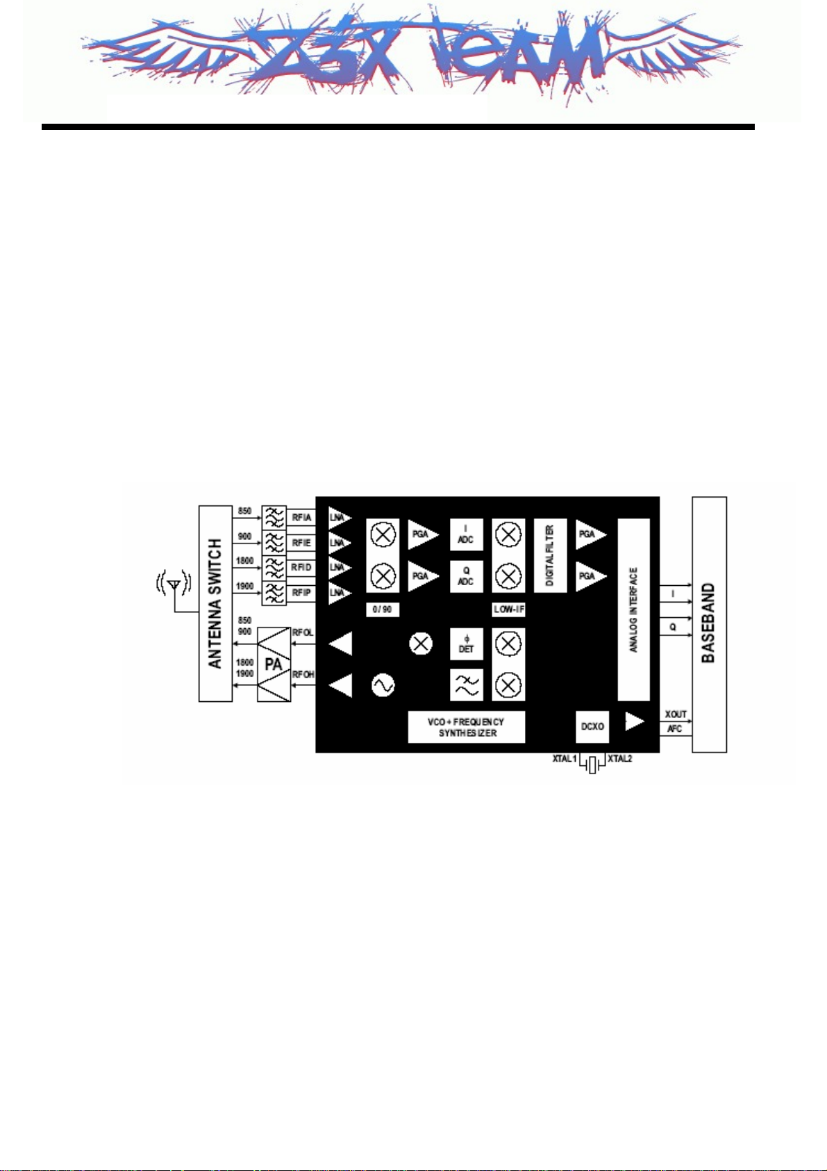
Figure 3-1 TOP LEVEL BLOCK OF MG120
The Figure 3-1 shows the top level block diagram of MG120, it contains
RF and BB part. The following list is the detailed.
1. AD6720:ADI baseband chipset,
2. PA+FEM:RF3166 is The PAM and HWXQ515 is the FEM
3. Transceiver: SI4210
4. Flash: Spansion 32Mb+64Mb
5. Others
A: 22 keys
B: 128*128 65K CSTN Main LCD and 96*64 MONO FSTN Sub LCD
C: Vibrator, Mic, Speaker, Ear-jack
D: Sim socket
E: Battery connector
Z3X-BOX.COM
- 15 -
3. TECHNICAL BRIEF
3.2 RF Part Introductions
The RF part consists of a power amplifier part, a transmitter
part, a crystal reference system, and an ant-switch part.
3.2.1 Power Amplifier (RF3166, U102)
The RF3166 is a high-power, high-efficiency power amplifier module with integrated power
control that provides over 50dB of control range. The device is a self-contained 6mmx6mm
module with 50Ω input and output terminals. The device is designed for use as the final RF
amplifier inGSM850, EGSM900, DCS and PCS handheld digital cellular equipment and
other applications in the 824MHz to849MHz, 880MHz to 915MHz, 1710MHz to 1785MHz
and 1850MHz to 1910MHz bands. The RF3166 incorporates RFMD’s latest VBATT tracking
circuit, which monitors battery voltage and prevents the power control loop from reaching
saturation. The VBATT tracking circuit eliminates the need to monitor battery voltage,
thereby minimizing switching transients. The RF3166 requires no external routing or
external components, simplifying layout and reducing board space.
Z3X-BOX.COM
Figure 3-2 Functional Block Diagram
- 16 -

3. TECHNICAL BRIEF
Figure 3-3 RF3166 PAM Pin Configuration-9-Pin
Table 3-1. RF3166 Pin Names and Signal Descriptions
PIN Function Description
1 DCS/PCS
IN
2 BAND
SELECT
3 TX
ENABLE
4 VBATT
5 GND
6 VRAMP
7 GSM IN
8 GSM OUT
9 DCS/PCS
OUT
Pkg
Base
GND
RF input to the DCS band. This is a 50ohm input
Logic Low enable GSM band Logic HIGH enable DCS/PCS band
Enable PA module for operation with a logic high
Power supply for the module
Ramping signal from DAC. No external filtering is required
50ohm input pin for GSM band
Z3X-BOX.COM
50ohm output pin for GSM band
50ohm output pin for DCS/PCS band
- 17 -
3. TECHNICAL BRIEF
3.2.2 Transceiver (SI4210, U103)
The SI4210 transceiver is a complete RF front end for multi-band GSM and GPRS wireless
communications. The receive section interfaces between the RF band-select SAW filters and
the baseband subsystem. The Aero II receiver leverages a proven digital low-IF architecture
and enables a universal baseband interface without the need for complex dc offset
compensation. The transmit section of Aero II provides a complete upconversion path from
the baseband subsystem to the power amplifier (PA) using an offset phase-locked loop (OPLL)
integrated with Silicon Laboratories’ patented synthesizer technology. All sensitive
components, such as TX/RF VCOs, loop filters, tuning inductors, and varactors are completely
integrated into a single integrated circuit. The Aero II transceiver includes a digitally-controlled
crystal oscillator (DCXO) and completely integrates the reference oscillator and varactor
functionality.
Z3X-BOX.COM
Figure 3-4 Functional Block Diagram
- 18 -

3. TECHNICAL BRIEF
Table 3-2. SI4210 Pin Names and Signal Descriptions
Pin Number(s) Name
1 SCLK Serial clock input
2 SEN Serial enable input ( active low)
3 SDIO Serial data input/output
4,5 BQP,BQN Transmit/receiver Q input/output
6,7 BIP,BIN Transmit/receiver I input/output
8 XOUT Clock output to baseband
9 PDN Power down input
10 RESET Reset pin
11 VIO Interface supply voltage
12,13,28,29 VDD supply voltage
14,PAD GND Ground
15 RFOL GSM 850 and EGSM 900 output
16 RFOH DCS 1800 and PCS 1900 output
17,18 RFIPP,RFIPN PCS 1900 LNA input
19,20 RFIDP,RFIDN DCS 1800 LNA input,
21,22 RFIEP,RFIEN EGSM 900 LNA input
23,24 RFIAP,RFIAN GSM 850 LNA input
25 XMODE DCXO/VC-TCXO mode enable
26 XDIV XOUT frequency select input
27 AFC Baseband analog AFC input
30,31 XTAL2,XTAL1 Crystal output and input
Z3X-BOX.COM
32 XEN XOUT pin enable
- 19 -
3. TECHNICAL BRIEF
3.2.3 FEM (HWXQ515,U104)
Table 3-3 Band SW Logic Table
Select Mode Vc(GSM) Vc(DCS/PCS)
GSM-Rx Low Low
GSM-Tx High Low
DCS-Rx Low Low
PCS-Rx Low Low
DCS/PCS-Tx Low High
3.2.4 26MHz Clock (TG-5000LA, X100)
The 26MHz clock (X100) consisits of a TCXO(Temperature Compensated Crystal Oscillator)
which oscillator at a frequency of 26 MHz. It is used within the RF part and DBB part.
Z3X-BOX.COM
- 20 -

3. TECHNICAL BRIEF
3.3 Baseband Introductions
3.3.1 Baseband Processor (AD6720 , U201)
• AD6720 is an ADI designed processor
• AD6720 consists of
1.Control Processor Subsystem including:
• 32-bit MCU ARM7TDMI Control Processor
• 39 MHz operation at 1.8V
• 1Mb of on-chip System SRAM Memory
2. DSP Subsystem including:
• 16-bit Fixed Point DSP Processor
• 91 MIPS at 1.8V
• Data and Program SRAM
• Program Instruction Cache
• Full Rate, Enhanced Full Rate and Half Rate
• Speech Encoding/Decoding
• Capable of Supporting AMR & PDC Speech Algorithms
3. Peripheral Functions
• Parallel and Serial Display Interface
• Keypad Interface
• Flash Memory Interface
• Page-Mode Flash Support
• 1.8V and 3.0V, 64 kbps SIM Interface
• Universal System Connector Interface
• Data Services Interface
• Battery Interface (e.g. Dallas)
4. Other
• Supports 13 MHz and 26 MHz Input Clocks
• 1.8V Typical Core Operating Voltages
• 289-Ball Package (12x12mm) , 0.65mm Ball pitch
5. The AD6720 baseband transmit section supports the following
• mobile station GMSK modulation power classes:
• GSM 900/850 power classes 4 and 5,
• DCS 1800 power classes 1 and 2, and
• PCS 1900 power classes 1 and 2
3.3.2 Interconnection with external devices
Z3X-BOX.COM
A. RTC block interface
Countered by external X-TAL
The X-TAL oscillates 32.768KHz
- 21 -
3. TECHNICAL BRIEF
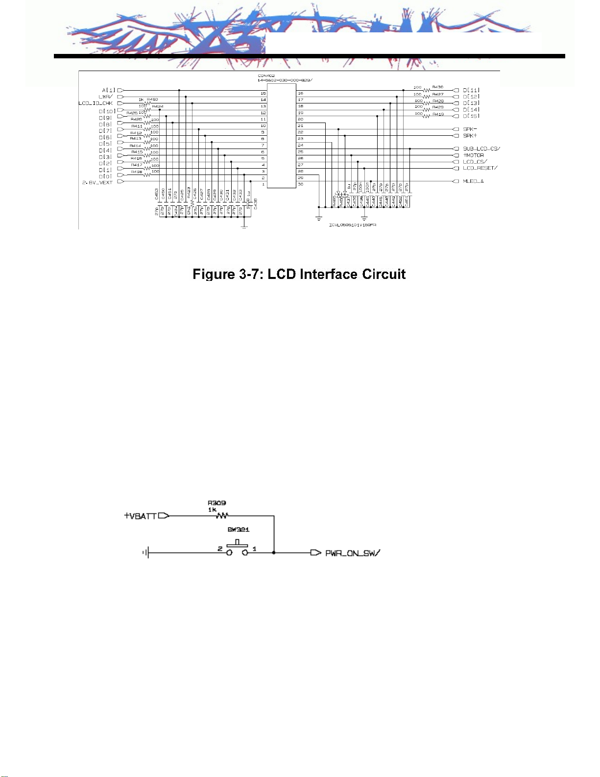
B. LCD module interface
Signals Description
LCD_CS/
LCD_REST/
LWR/
SUBLCD_CS/
LCD_ID_CHK
A1
Table 3-4: LCD Pin Description
The backlight of LCD module is controlled by AD6720 via AAT3122, U301.The
Control signals related to Backlight LED are given bellow.
Main LCD driver chip enable.
Thos pin resets LCD module.
Enable writing to LCD Driver.
SUB LCD Driver chip enable
This pin determines the LCD module type
Select 16bits interface mode for MAIN LCD
Signals Description
LCD_BACK_EN Control LCD backlight in 2 steps
MLED_A Current source backlight LED
Table 3-5: LCD Backlight LED Control
There are two steps of the LCD back light setting, bright and middle level,
this two levels setting will save power in some condition.
Z3X-BOX.COM
C. RF interface
The AD6720 control RF parts through PA_BAND, ANT_SW1, ANT_SW2,
CLKON , PA_EN, S_EN, S_DATA, S_CLK, RF_PWR_DWN.
- 22 -
3. TECHNICAL BRIEF
Signals Description
PA_BAND PAM Band Select
ANT_SW1 Antenna switch Band Select
ANT_SW2 Antenna switch Band Select
RF_PWR_DWN Power down input
CLKON RF LDO Enable/Disable
PA_EN PAM Enable/Disable
S_EN PLL Enable/Disable
S_DATA Serial Data to PLL
S_CLK Clock to PLL
Table 3-6. RF Control Signals Description
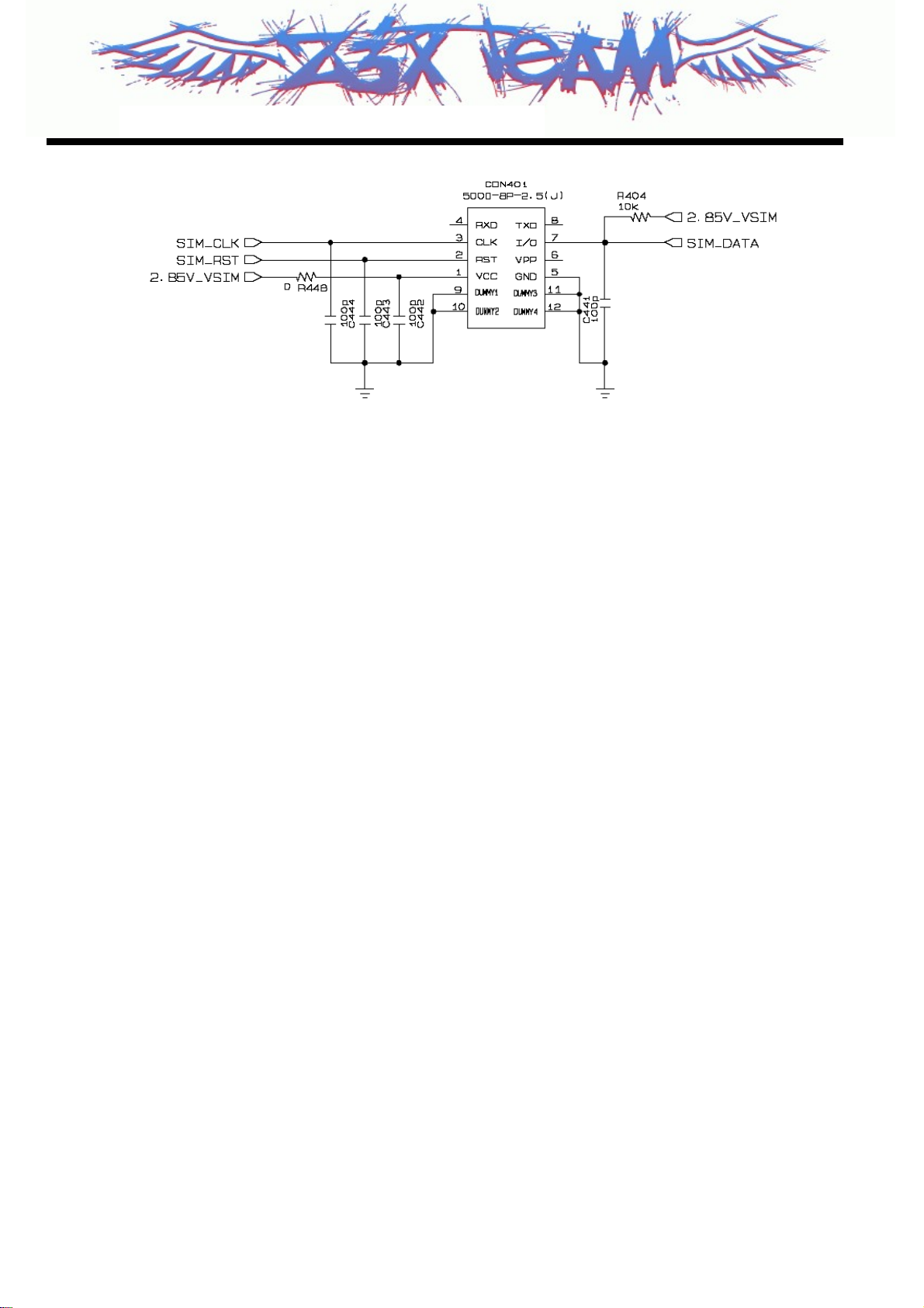
D. SIM interface
The AD6720 provides SIM Interface Module. The AD6720 checks status periodically
during established call mode whether SIM card is inserted or not, but it doesn't check
during deep Sleep mode. In order to communicate with SIM card, 3 signals SIM_DATA,
SIM_CLK, SIM_RST(GPIO_23) are required. The descriptions about the signals are
given by bellow Table 3-7 in detail.
signals Description
SIM_DATA This pin receives and sends data to SIM
SIM_CLK Clock 3.25MHz frequency
SIM_RST Reset SIM block
Z3X-BOX.COM
Table 3-7: SIM Control Signals Description
card. This model can support only 3.0 volt
interface SIM card.
- 23 -
3. TECHNICAL BRIEF
Figure 3-5: SIM Interface of AD6720
E. LDO Block
There are 8 LDOs in the AD6720.We only use 7 of them.
-VCORE : supplies Digital baseband Processor core and AD6720 digital core
-VMEM : supplies external memory and the interface to the external memory on the
digital baseband processor (1,8V or 2.8V, 150mA)
-VEXT : supplies Radio digital interface and high voltage interface (2.8V, 170mA)
-VSIM : supplies the SIM interface circuitry on the digital processor and SIM card (2.85V,
20mA)
-VRTC : supplies the Real-Time Clock module (1.8 V, 20A)
-VMIC : supplies the microphone interface circuitry (2.5 V, 1 mA)
-VVCXO : supplies the voltage controlled crystal oscillator ( 2.75 V, 10 mA)
Z3X-BOX.COM
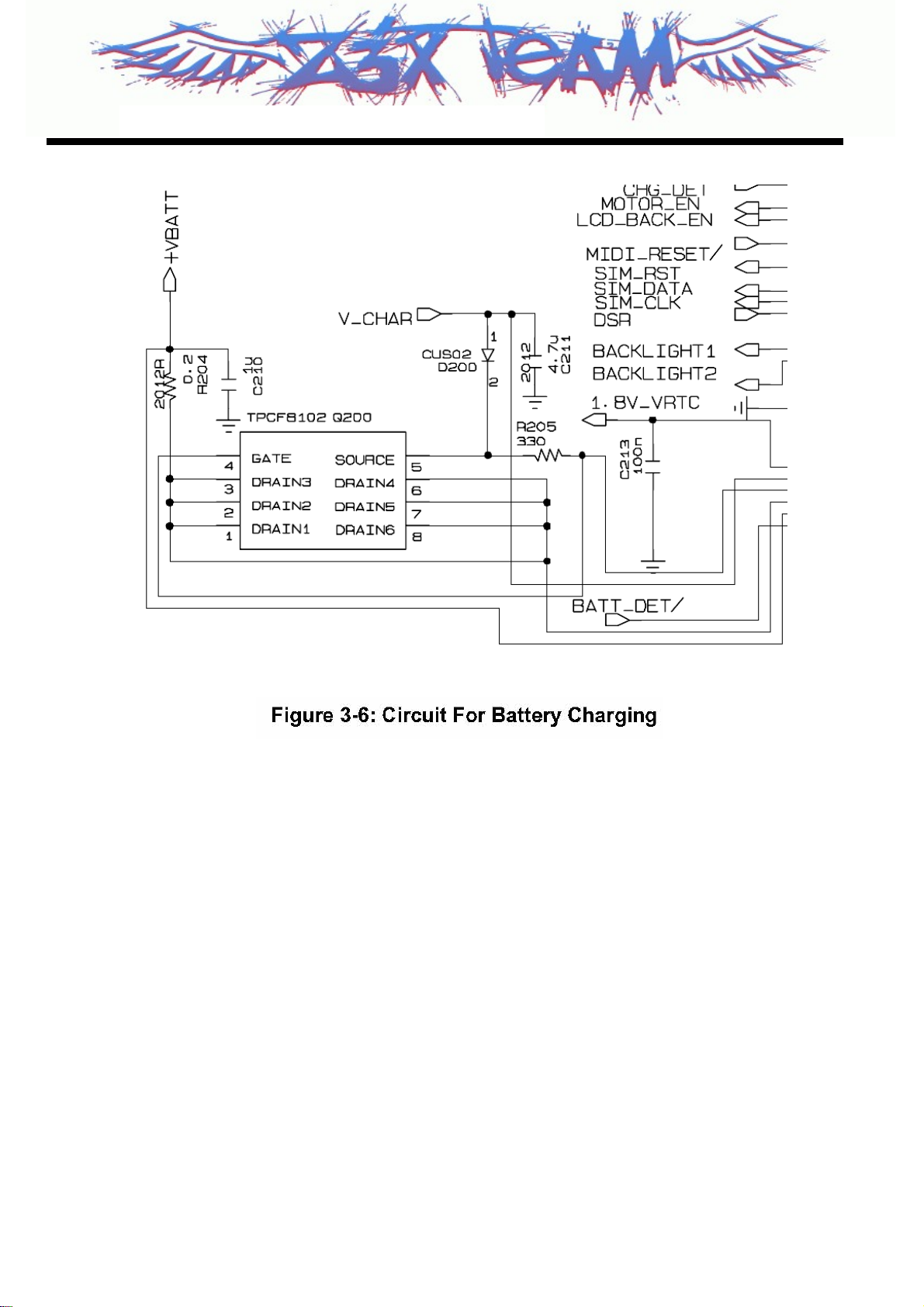
3.3.3 Battery Charging Block
1. It can be used to charge Lithium Ion batteries. Charger initialization, trickle
charging, and Li-Ion charging control are implemented in hardware.
- 24 -
2. Charging Process
-Check charger is inserted or not
-If AD6720 detects that Charger is inserted, the CC-CV charging starts.
-Exception : When battery voltage is lower than 3.2V, the precharge low current
charge mode) starts firstly.
-And the battery voltage reach to 3.2V the CC-CV charging starts.
3. Pins used for charging at the AD6720 side.
-VCHG : charger supply.
-GATEDRIVE : charge DAC output
-ISENSE : charge current sense input
-VBATSENSE : battery voltage sense input.
-BATTYPE : battery type identification input
-REFCHG : voltage reference output
4. TA (Travel Adaptor)
-Input voltage: AC 85V ~ 260V, 50~60Hz
-utput voltage: DC 5.2V ( 0.2 V )
-Output current: Max 800mA ( 50mA )
5. Battery
-Li-ion battery (Max 4.2V, Nom 3.7V)
-Standard battery: Capacity - 830mAh
3. TECHNICAL BRIEF
Z3X-BOX.COM
- 25 -
3. TECHNICAL BRIEF
3.3.4 Display and Interface
• Main LCD&SUB LCD
Controlled by LCD_CS/,SUB_LCD_CS/,LCD_RESET/,LWR/,LCD_ID_CHK,
D[0:15] ports
• LCD_CS/ : MAIN LCD driver chip enable. MAIN LCD driver IC has own
CS pin
• LCD_RESET/ : This pin resets LCD module. This signal comes from AD6720 directly.
• SUB_LCD_CS: SUB LCD driver chip enable. SUB LCD driver IC has own CS pin
• LWR/ : Write control Signal .
• D[0:15] : Parallel data lines.
• LCD_ID_CHK: LCD type selection signals
• For using 65K color, data buses should be 16 bits.
Properties Spec. Unit
Active Screen Size 35.78*39.7*4.8 mm
Color Depth 65,536 colors
Resolution 128 X RGB X 128 dots
SUB LCD B/W 96*64 FSTN
Z3X-BOX.COM
- 26 -
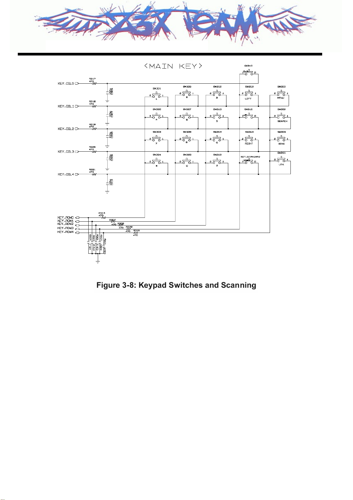
3.3.5 Keypad Switches and Scanning
3. TECHNICAL BRIEF
The key switches are metal domes, which make contact between two concentric pads on
the keypad layer of the PCB when pressed. There are 21 switches, connected in a matrix
of 5 rows by 5 columns and additional GPIO 35 for KEY_ROW5, as shown in Figure 3-8,
except for the power switch (KB1), which is connected independently. Functions, the row
and column lines of the keypad are connected to ports of AD6720. The columns are
outputs, while the rows are inputs and have pull-up resistors built in. When a key is
pressed, the corresponding row and column are connected together, causing the row
input to go low and generate an interrupt. The columns/rows are then scanned by
AD6720 to identify the pressed key.
KEYPADON
Z3X-BOX.COM
- 27 -
3. TECHNICAL BRIEF
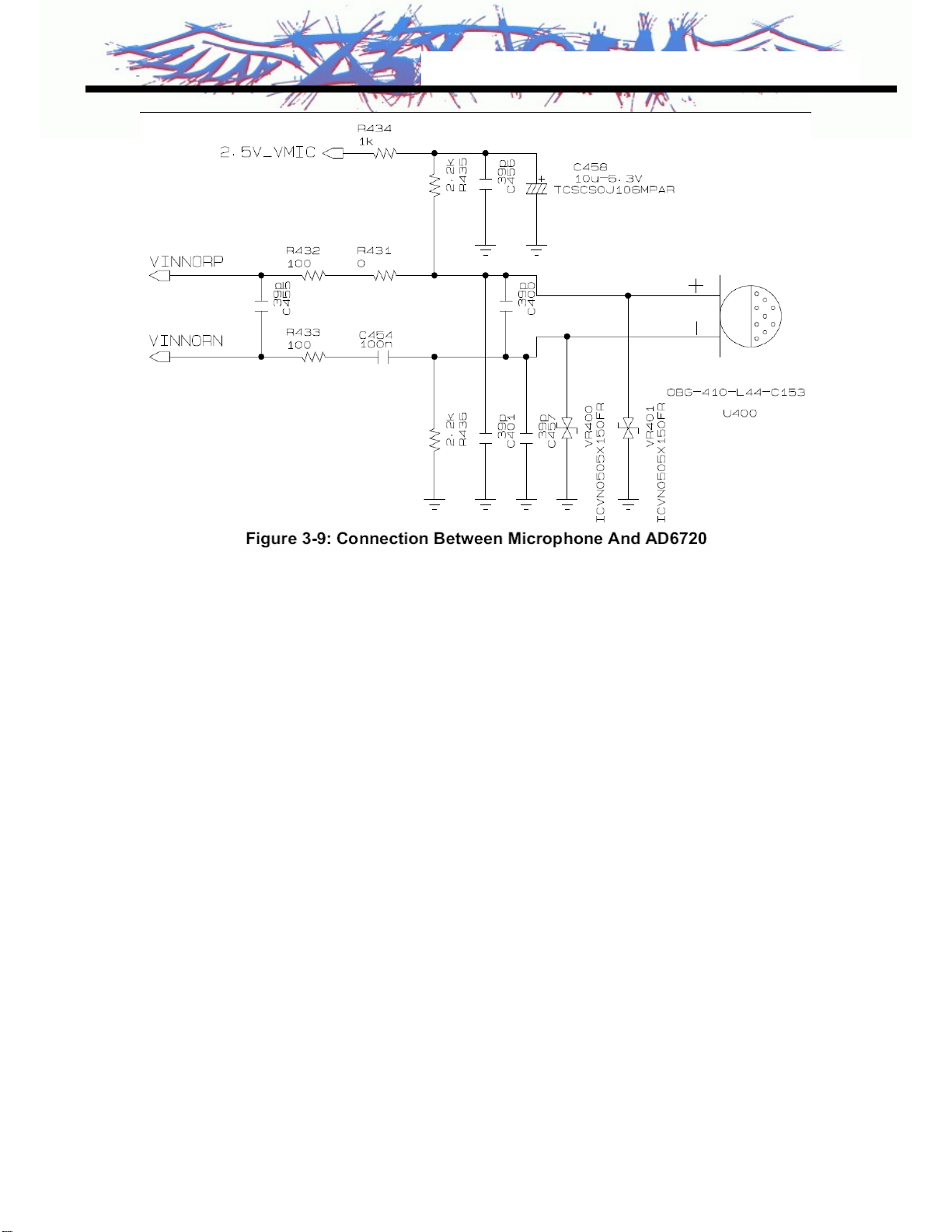
3.3.6 Microphone
The microphone is placed to the A side of PCB. The audio signal is passed to VINNOP
and VINNON pins of AD6720. The voltage supply VMIC is output from AD6720, and is a
biased voltage for the VINNOP. The VINNOP and VINNON signals are then A/D
converted by the voiceband ADC part of AD6720.The digitized speech (PCM
8KHz ,16KHz) is then passed to the DSP section of AD6720 for processing (coding,
interleaving etc).
Z3X-BOX.COM
- 28 -
3. TECHNICAL BRIEF
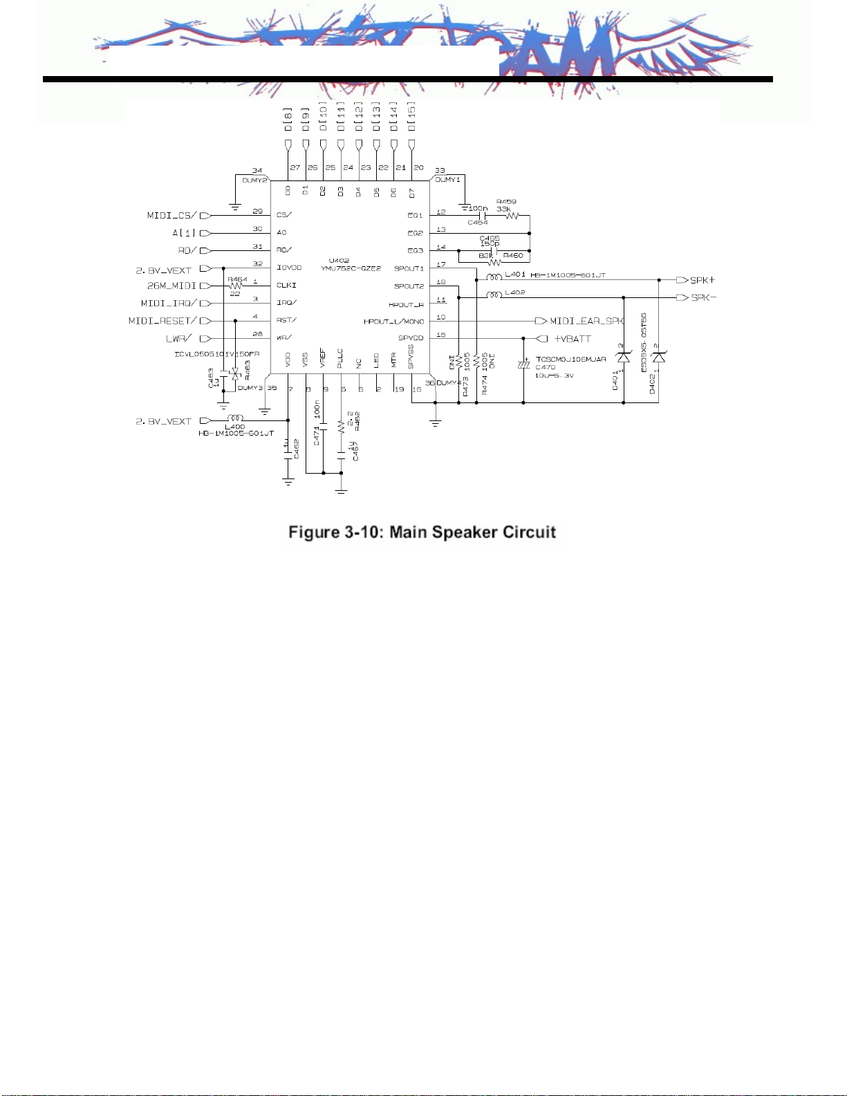
3.3.7 Midi and Main Speaker
The Vimicro MIDI IC VC0917 Solution MIDI music player solution offering the following
features:
_ MIDI standards compliant
_ MIDI files playable as polyphonic ringtones
_ 40 notes polyphony
Z3X-BOX.COM
_ MIDI file parser supports Standard MIDI (formats 0, 1 and 2), WAV.
The main speaker is driven directly by vc0917 SPOUT1 and SPOUT2 pins
- 29 -
3. TECHNICAL BRIEF
3.3.8 Headset Interface
This type supports mono sound.
Switching from Receiver to Headset Jack
If jack is inserted, EAR_SENSE/ goes from high to low.
Audio path is switched from receiver to earphone by EAR_SENSE/ interrupt.
Switching from Headset Jack to Receiver
If jack is removed, EAR_SENSE/ goes from low to high.
Audio path is switched from earphone to receiver by EAR_SENSE/ interrupt.
Z3X-BOX.COM
- 30 -
 Loading...